Article

Ideal HTLs May Open the Door for Further Development of Sb2Se3 Solar Cells—A Numerical Approach

1
Academy of Scientific and Innovative Research (Asir), Ghaziabad 201002, India
2
CSIR-National Physical Laboratory, Indian Reference Materials (BND) Division, Dr. K. S. Krishnan Marg, New Delhi 110012, India
*
Authors to whom correspondence should be addressed.
Sustainability 2023, 15(13), 10465; https://doi.org/10.3390/su151310465
Submission received: 22 May 2023 / Revised: 29 June 2023 / Accepted: 2 July 2023 / Published: 3 July 2023
(This article belongs to the Special Issue Advance in Energy Materials for Sustainability)

Abstract

:
Antimony selenide (Sb2Se3) material has been brought into sharp focus in the solar cell field due to its remarkable performance in recent times. Solar cell efficiency increases daily because of the excellent properties of Sb2Se3 material and progressive optimisation of each layer, especially the hole-transporting layer (HTL); it suppresses the recombination of the back surface and increases the built-in potential and efficiency. In this work, we used Sb2Se3 as an absorber layer and compared the behaviour of typical hole transport materials (HTMs) (Spiro-OMeTAD, CuSCN, and CuI) and their influence on device performance. The Sb2Se3 photovoltaic model with different HTMs was studied by SCAPS (version 3.3.10) software. Efficiency is highly influenced by light source and intensity. Thickness and defect density of the Sb2Se3 layer, the work function of the back contact, and series and shunt resistances also play an essential role in the better execution of solar cells. The performance of the device is enhanced when the transmission percentage increases at the front contact. The metalwork function must be 5 eV to attain a highly efficient PV cell, and after optimisation, CuI is the best HTM with a 23.48% efficiency.
Keywords:
HTL; simulation; Sb2Se3; SCAPS

1. Introduction

In recent times, the use of energy has increased dramatically with the fast growth of the social economy. So, there is a need to investigate renewable, durable, effective, and clean energy resources as alternatives to traditional fossil fuels, and solar energy is one of the most suitable alternatives. Sb2Se3 has been considered a widely used absorbing material because of its optimal bandgap [1], higher absorption coefficient [2], nontoxic nature, and lower cost. Sb2Se3 is not listed as a hazardous material by the regulatory authorities in the United States, European Union, or China. Sb2Se3 has strong physiochemical stability, and the quantity of Sb and Se elements in the Earth’s crust is 0.2 and 0.05 ppm, respectively. Thin-film absorber morphology and proper band alignment between constituent layers must be considered. Three important requirements must be satisfied by the solar cell absorber layer: (i) an excellent charge carrier transport property for collecting photogenerated carriers prior to recombination; (ii) excellent charge carrier transport characteristics; and (iii) a consistent and strong internal electric field within the junction to guarantee electron-hole pair separation. Many reports on hole transport materials (HTMs) have shown the significant impact of hole transport layers (HTLs). Many researchers have suggested that an HTL may be advantageous in reducing the carrier recombination loss at the rear surface to improve PV performance. When constructing solar cells, intrinsic HTL characteristics, like strong carrier mobility and good p-type conductivity, are essential, but the Sb2Se3/HTL energy-level matching and HTL/back contact are also important. However, inefficient carrier transport and collection, in addition to interface recombination with many HTLs, still lead to a deficit of open-circuit voltage and short-circuit current, contributing to low PV efficiency.
Holes in the active layer are extracted and transported to the electrode by this HTL layer. It also prevents electron transport toward the anode [3]. Low price and simple preparation of HTMs should also be considered for the scalable manufacture and future commercial application [4,5,6,7]. 2,2′,7,7’-Tetrakis[N, N-di(4-methoxyphenyl)amino]-9,9’-spirobifluorene (Spiro-OMeTAD) [8] is the popular organic HTM for up-and-coming solar devices. Spiro-OMeTAD has a higher glass transition temperature, amorphous nature, and appropriate energy levels [3]. Despite organic small-molecular HTLs being simple to manufacture, one of the barriers to widespread commercial manufacturing has been the stability of organic components. Different inorganic materials with high stability have been studied to address the stability concerns and device performance deterioration caused by organic HTLs. P-type HTMs, such as CuI and copper-thiocyanate (CuSCN), have a band gap of 3.1 eV and 3.4 eV, respectively, and show good stability, high hole mobility, good transparency in the visible spectrum, and ease of manufacture [9,10]. Still, its inferior photovoltaic nature can damage the absorber layer during coating. Jung et al. used a CuSCN-made HTL on the front of the ITO substrate with a simple solution process approach for a better planar heterojunction PV cell with 10% efficiency [11]. Li. Kanghua et al. also used CuSCN as an HTL layer for Sb2Se3-based photovoltaic cells and obtained an efficiency of 7.5% [12]. It reduced the recombination loss of charge at the HTL/absorber layer interface. Here, we analysed the performance of Sb2Se3-based photovoltaic cells for various HTMs, including Spiro-OMeTAD, CuI, and CuSCN, by SCAPS simulator. For only one-dimensional solar cells, SCAPS (Version 3.3.10) software can be utilised to simulate them accurately. The absorber layer thickness, total defect density, shallow acceptor density, and back contact metal work function were systematically studied.
SCAPS’s main work is to resolve one-dimensional semiconductor equations. The simulator worked on the simultaneous resolution of equations for electrons and holes [13,14,15], as shown in Equations (1)–(3).
2 Ψ x 2 + q ε   [ p ( x ) n ( x ) + N D N A + ρ ( n , p ) ] = 0
1 q d J n d x = ( G R )
1 q d J p d x = ( G R )
Here, Ψ is electrostatic potential, ε is the permittivity, q is the electron charge, n(x), p(x), and ρ shows the concentration of electrons, holes, and density of charge carriers. ND and NA are donor and acceptor impurities, R and G are recombination and generation rates, and Jn and Jp are the current densities of electrons and holes.
The following Equations (4) and (5) are used to define the transportation of carriers in semiconductors by drift and diffusion:
J n = µ n n q E F n x
J p = µ p p q E F p x
Here, EFp and EFn are the p- and n-type carrier fermi levels, and µn and µp are the electron and hole mobility, respectively.
The current–voltage (I–V) characteristic is obtained by simulating the parameters. The I–V parameters are open-circuit voltage (Voc), short-circuit current density (Jsc), fill factor (FF), and efficiency (η). The Voc value is calculated by taking the net current zero, as shown in Equation (6).
V O C = k T q ln ( I L I O + 1 )
Here, Io and IL are the saturated current and generated light, respectively, and Voc depends on both Io and IL
Efficiency is defined as the ratio of output (Pmax) to input power (PS), as defined in Equation (7).
η = J m a x V m a x P s
Here, Pmax = JmaxVmax, and Ps is the sunlight’s incident power, and Jmax and Vmax are the maximum short-circuit current and open-circuit voltage, respectively. Apart from Voc and efficiency, FF is also an essential measurement for solar cell working, as shown in Equation (8) below.
F F = J m a x V m a x J s c V o c
Apart from the I–V characteristic, current–voltage (C–V) characteristics give an in-depth idea about the performance of a photovoltaic device. Built-in voltage (Vb) parameters can be determined from the capacitance–voltage, and a greater Vb means an increased driving force for charge carrier separation that results in a larger Voc for Sb2Se3-based solar devices.
SCAPS is very sensitive to the input parameters as the software solves the equation numerically with appropriate boundary and initial conditions. The most likely causes of convergence failure are contact characteristics, layer electron affinities, defect concentrations, defect energy distributions, and mobility values outside the expected range. In addition to these, a little change in the Nc, Nv, ND, NA, or Eg values can typically affect the device’s performance. Each layer’s input parameters need to be double-checked, and the values must be changed to realistically attainable ones. Because Sb2Se3 is still in its infancy, simulations are crucial to perform to save the researchers’ time and energy when optimising the characteristics of materials and devices. For the program to calculate the simulation results in a fair amount of time, it must operate under a set of approximations, assumptions, and constraints.
A favourable energy band alignment is crucial in determining the device performance of Sb2Se3 solar cells. According to this viewpoint, the enhancement of energy band alignments by using ideal HTLs may open the door to developing Sb2Se3 solar cells.

2. Device Structure and Simulation Parameters

The device structure consists of Sb2Se3 (absorber layer), spiro-OMeTAD, CuSCN, CuI (HTMs), ZnO (window layer), CdS (ETL layer), and molybdenum (back contact). They are schematically illustrated in Figure 1a. The energy potential of the layers is shown in Figure 1b. A constant light of 1000 W/m2 at AM1.5G and temperature of 300 K are used.
Material parameters of each layer for simulation were taken from the literature [16,17,18] as summarised in Table 1. The absorber layer absorption coefficient must be high (~105 cm−1) to effectively produce electron-hole pairs. The absorption coefficient of the absorber layer was set as 105 cm−1, and its thickness varied from 0.6 to 1.6 µm. The absorber layer band gap should match the solar spectrum for PV applications. If the band gap is too big, many photons with insufficient energy will pass through the material without creating an electron-hole pair. Electron affinity determines the conduction band offset at the interface between the two semiconductors. The offset substantially impacts the short-circuit current, open-circuit voltage, and overall performance of the solar cell. One of the crucial elements of electrical devices is the mobility of the charge carrier in the semiconductor. It describes the material’s ability to conduct charge carriers as an external electric field is applied. The total defect density of the active layer is an additional factor that could significantly impact the device’s performance. The quality of interfaces and the development of defects impact the performance of thin-film solar cells.
The thermal velocity of electrons-holes was kept constant at 107 cm s−1. The absorber layers’ total defect density (Nt) varied, whereas it was fixed for other layers. Nt for Sb2Se3 varied from 1013 to 1017 cm−3. Nt for CdS and ZnO was taken as 1014 cm−3. The absorption coefficient for ZnO and CdS was 105 cm−1. Layer defects were also added (Table 2) to produce real device conditions. Properties introduced for back and front contacts are shown in Table 3.

3. Results and Discussion

The present work is aimed at how different HTMs can vary the efficiency when the absorber layer thickness, total defect density, and shallow acceptor density are varied. A back contact work function also changed the performance of the device. After optimising various parameters, the energy band structure was studied to check the photovoltaic cell efficiency.

3.1. Effect of Antimony Selenide Material Thickness

An absorber layer thickness is critical in optimising a photovoltaic cell. The absorber layer thickness is taken from 0.6 to 1.6 µm to check its influence on the cell’s different I–V parameters for three different HTM-based structures, as shown in Figure 2. At a 1.0 µm absorber layer thickness, the highest efficiency is achieved for all three different structures. Jsc and Voc remain the same (0.93 V and 30.4 mA/cm2, respectively) for Spiro-OMeTAD and CuSCN. FF and efficiency for Spiro-OMeTAD, CuI, and CuSCN changed with the absorber thickness. The results show that the thickness should be selected carefully to increase the current density, as a thin film will not allow the absorption of enough incident light. Similarly, when the thickness exceeds an optimised value, the travelling path of the photoproduced charge carriers becomes too long, resulting in more carrier recombination.
Thus, we used 1.0 µm as an optimised value for the absorber layer thickness. The CuSCN-based cell shows 18% efficiency (Voc = 0.93 V, Jsc = 30.46 mA/cm2, and FF = 63.17%). For Spiro-OMeTAD, the maximum efficiency is 21.15% (Voc = 0.93 V, Jsc = 30.47 mA/cm2, and FF = 74.08%) mA/cm2, and among all the three HTMs, CuI attained the highest efficiency of 23.48% (Voc = 0.93 V, Jsc = 30.47 mA/cm2, and FF = 82.29%).

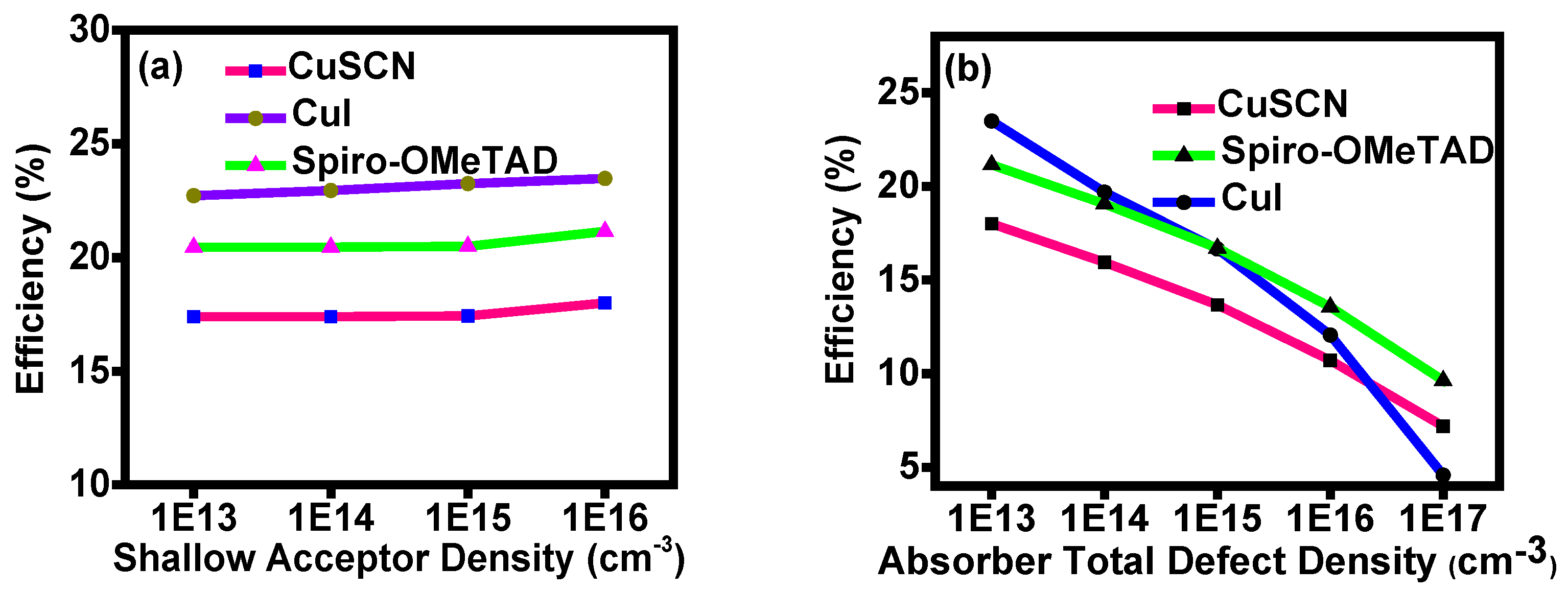
3.2. Acceptor and Total Defect Density of Sb2Se3 for Various HTMs

Many impurities during the growth of the absorber probably enhance the density of acceptors within it. Doping the absorber with sodium diffusing from the soda glass substrate is the most common. To optimise the device’s performance, the dopants should be under control because, at high concentrations, they may shorten the charge carriers’ lifetime by reducing mobility. If the acceptor density is low, it can increase the series resistance, and if it is higher, it can decrease the shunt resistance and, overall, reduce the solar cell’s performance. Therefore, an optimised acceptor density should be maintained.
The efficiency increased from 22.72% to 23.48%, 17.4% to 18%, and 20.46% to 21.15% for CuI, CuSCN, and Spiro-OMeTAD, respectively, when the acceptor density was varied from 1013 to 1016 cm−3 as shown in Figure 3a. Grain boundaries cause harmful deep levels in Si and CdTe but do not affect CIGS, CZTSe, or CZTS [19]. Higher defect concentrations in the absorber layer would increase the recombination due to the formation of pinholes, faster rate of film deterioration, less stability, and lower overall device performance. Thus, to analyse the defect density (Nt) performance, defect density values vary from 1013 to 1017 cm−3 in the absorber layer, and at 1013 cm−3, maximum efficiencies are obtained for all the HTMs. The enhancement in defect density value decreased efficiency for all three HTMs, as depicted in Figure 3b. When the defect density increases, the carrier recombination rate will also increase, the carrier lifespan and diffusion length will decrease; and the overall performance will decrease [18,20]. Hu et al. investigated electrically active defects in Sb2Se3 thin-film solar cells. Three defects were found, two of which were bulk-type, while the third was an interface or near-interface defect [21]. Wen et al. found that the defect density (Nt) for Sb2Se3 solar cells deposited by the VTD and RTE methods are 1014 cm−3 and 1015 cm−3, respectively [22]. Keeping the Sb2Se3 defect density as low as possible will help the Sb2Se3 devices perform better in the experiment.

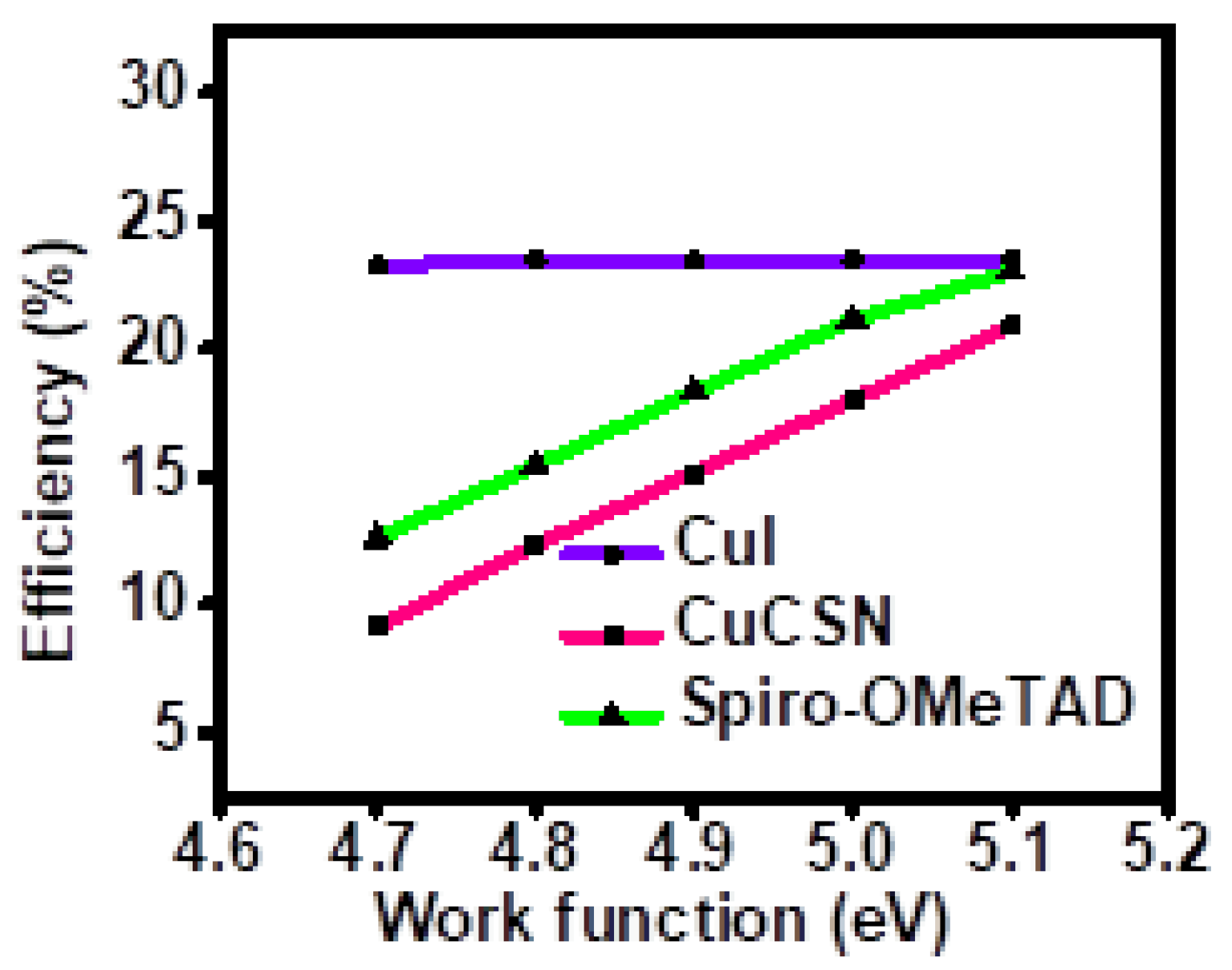
3.3. Effect of Various Back Contact Materials on Device Efficiency

The back contact is also a main parameter behind a solar device’s excellent performance, as it helps to achieve a better built-in voltage (Vb). A back contact with a larger work function value improves energy band alignment [23]. Many researchers used gold (Au) as a back contact [24,25,26,27]. The use of Au contacts is only justifiable on a small scale and with small-area devices. The solar cell technology that relies on large-area devices, Au contacts, will increase the overall fabrication cost of the device. Less-expensive materials can effectively replace Au contacts for a better-performing device. Graphite is also used as the back electrode, is lower in cost than Au, and can produce an efficient solar cell [28]. A Sb2Se3 solar cell with molybdenum (Mo) as the back electrode has also shown excellent performance with a 9.2% efficiency [29]. Different materials have different work function values, such as Ag, Cr, Cu, Ni, Au, Pt, and Fe, with work functions of 4.26 eV, 4.5 eV, 4.6 eV, 5.2 eV, 5.1 eV, 5.65 eV, and 4.8 eV, respectively [30]. Ni has a high work function value that only applies to Ni’s single crystal and a different value for thin-film structures produced on rough surfaces. Ni’s work function will be as low as 4.44 eV [31]. In this numerical study, the back contact work function varies from 4.6 to 5.2 eV to check the impact on the solar device performance, as shown in Figure 4. For all three HTMs, efficiency was low, below 4.8 eV. A lower work function value can negatively affect the device’s performance because of a significant energy-level mismatch, resulting in the formation of the Schottky junction, which decreases the device’s efficiency [32]. In the case of all HTMs, the efficiency increases dramatically with the values of work functions. The highest efficiencies of 23.48%, 20.87%, and 23.02% are achieved for CuI, Spiro-OMeTAD, and CuSCN, respectively, when the work function value is 5.1 eV. We used 5.0 eV (Mo) as an optimised value for the back contact.

3.4. Effect of Series and Shunt Resistances

The series (RS) and shunt resistances (Rsh) significantly influence the device’s performance. Shunt and series resistances are examples of parasitic components showing solar cell losses. A large value of Rs decreases the short-circuit current (Jsc), whereas a smaller value of Rsh results in less open-circuit voltage (Voc). As a result of these opposing effects, the fill factor falls and poor power conversion efficiency results. When the bias was reversed, a large current began to flow at a relatively low applied voltage. The increased leakage current is due to a shorter charge transport pathway through the extremely thin layer, significantly lowering the junction’s shunt resistance. The semiconductors’ bulk resistance and metal contact resistance are additional sources of series resistance, while the interface and bulk semiconductor flaws are the main causes of shunt resistance.
The photovoltaic cell’s I–V parameters are decreased by series resistance. The defect states decrease as the device’s shunt resistance increases because recombination in the defect states is the main cause of shunt resistance [33,34]. Figure 5a shows that as the series resistance varies from 1.0 to 5.0 ohm·cm2, the power conversion efficiency values drop with an increase in series resistance. Similarly, the shunt resistance varies from 300 to 1500 ohm-cm2, and the efficiency increases with shunt resistance, confirming previous study results [35]. This simulation study thoroughly optimises ideal devices without considering Rs and Rsh resistances. In an ideal solar device, the series and shunt resistances are zero and infinite, respectively.

3.5. Impact of the Transmission Filter and Light Spectrum on the Device

At the front contact, the transmission filter can be adjusted. The transmission filter varies from 10% to 90%, as shown in Figure 6a. The efficiency increases when the transmission percentage increases. The optimised percentage of transmission at the front contact was 80%. Figure 6b shows that the efficiency is highly influenced by light source and intensity. The sunlight comprises the complete spectrum of radiation. However, only light with a suitable wavelength will result in photovoltaic effects. It indicates that just a portion of the solar spectrum may be used to produce electricity. The wavelengths that are not absorbed do not result in electron-hole pairs, making them useless for photovoltaics. They merely generate heat, which can lower the cell’s efficiency. Solar cells need specific light spectrum wavelengths to produce electricity. Depending on the quantum features, the material is sensitive to various wavelengths. Due to this, efficiency will drop if the wavelength is very small or large. Based on the findings and the facts, the solar spectrum has various wavelengths and energies. The solution is to employ particular materials with their electrical properties as the proper optical filter, allowing the necessary wavelengths to pass through the solar cell. The standard illumination, AM1_5G 1 sun (1000 W/m2) spectrum, was used for the optimised structure for all three HTMs, and this is the default illumination spectrum in SCAPS.

3.6. Energy Band Diagram and I–V and C–V Characteristics

An energy band diagram depicts the energy levels and their respective positions. The diagram for Mo/Spiro-OMeTAD/Sb2Se3/CdS/ZnO under optimised conditions is shown in Figure 7a. When photogenerated carriers separate at an interface of the absorber and ETL layers, a high electric field accelerates them. It causes them to be drawn away from the junction quickly. Holes flow through the absorber and HTL layer and are trapped by Mo, and the electrons flow toward the ETL layer. This work considers the energy band structure for the Spiro-OMeTAD-based design, whose thickness is 0.05 µm. The thickness of other layers, such as the absorber, ETL, and window layer, is 1.0 µm, 0.05 µm, and 0.2 µm, respectively. Figure 7b depicts the simulated I–V characteristic of three HTM-based structures. The CuSCN-based cell shows an 18% efficiency (Voc = 0.93 V, Jsc = 30.46 mA/cm2, and FF = 63.17%). For Spiro-OMeTAD, the maximum efficiency is 21.15% (Voc = 0.93 V, Jsc = 30.47 mA/cm2, and FF = 74.08%), and among all the HTMs, CuI showed the highest efficiency of 23.48% (Voc = 0.93 V, Jsc = 30.47 mA/cm2, and FF = 82.29%). From the figure, we can see that CuI shows the highest efficiency. Due to the current–voltage (C–V) characteristic, a solar device can expose its more fundamental features. Here, the C–V plots for three various hole transport layers are examined. Equation (9) provides the relationship between the capacitance area and the depletion area as
1 C 2 = 2 ( V b V d c ) q ε N A A 2
Permittivity is denoted here by ε, built-in voltage by Vb, acceptor density by NA, and direct current voltage by Vdc.
Figure 7c displays a Mott–Schottky plot derived using the C–V characteristics. The depletion zone of the device with a higher Vb is more significant than that of the device with a lower Vb (where photogenerated carriers selectively move to their counter electrodes). As a result, the apparatus can segregate excitons and collect photogenerated carriers. Here, the CuI also shows the best performance compared to other HTLs. Table 4 shows the device’s performance with the help of different parameters, including Voc, Jsc, FF, and efficiency at optimised conditions.

3.7. Overall Performance and Optimised Parameters

Figure 8 shows the Sb2Se3-based photovoltaic cell performance for all HTM-based solar structures. CuI offers the highest efficiency among all the layers, so we chose this HTM for the energy band structure. In Table 5, the optimised parameters are summarised. The present results were compared with other Sb2Se3-based solar cells obtained experimentally and theoretically, as shown in Table 6.
Other methods, such as a sun tracker or a solar concentrator, can be used to boost the device’s performance even more. The peak power point of solar material also varies with incident light in a solar tracker. A maximum power point tracker can continuously measure the voltage and current to keep track of the instantaneous power in expensive and massive systems. As the photongenerated carriers increase due to an increase in light intensity, a solar concentrator is another technique to improve the performance of solar cells.
High thermal temperatures and moisture have always been major problems with device stability. By increasing the electrical resistance, ultraviolet light also undermines the stability of solar cells. The stability of the device is sometimes significantly impacted by the thickness of the electrodes.

4. Conclusions

In this work, after optimising the various parameters and effects of different HTMs on the device performance, we obtained a highly efficient Sb2Se3-based solar cell. We compared three different organic and inorganic hole transport materials using the SCAPS-1D simulator. Under the working temperature of 300 K and illumination of AM 1.5 G, the Sb2Se3 absorber layer thickness varies from 0.6 to 1.6 µm. The back contact work function, defect density, acceptor density, and absorber layer thickness affect the device’s performance. A work function for the back contact should be greater than 4.8 eV for higher efficiency. The efficiency increases when the transmission percentage increases. The optimised percentage of transmission at the front contact was 80%. The standard illumination, AM1_5G 1 sun (1000 W/m2) spectrum, was used for the optimised structure for all three structures. The light intensity also influences solar device efficiency, and this is also greatly influenced by the light spectrum because the materials employed are susceptible to various wavelengths due to their inherent quantum qualities. The optimised value of the shallow acceptor density for CuI, CuSCN, and Spiro-OMeTAD was taken as 1016 cm−3. Moreover, the absorber layer’s defect density (Nt) is optimised at 1013 cm−3. After optimising the parameters, it was found that CuI showed the highest efficiency of 23.48%. A favorable energy band alignment is crucial in determining the device performance of Sb2Se3 solar cells. According to this viewpoint, the enhancement of energy band alignments through the use of ideal HTLs may open the door for further development of Sb2Se3 solar cells.

Author Contributions

M.: Conceptualisation, methodology, data curation, and writing—original draft; R.K. (Raman Kumari) and R.K. (Rahul Kumar): Methodology; K.K.M.: Supervision and writing—review and editing; V.N.S.: Supervision and writing—review and editing. All authors have read and agreed to the published version of the manuscript.

Funding

No funding was acquired for this research publication.

Institutional Review Board Statement

Not applicable.

Informed Consent Statement

Not applicable.

Data Availability Statement

Data will be made available upon request with proper justification.

Acknowledgments

Mamta highly acknowledges the Council for Scientific and Industrial Research (CSIR), India, for the Senior Research Fellowship (SRF) grant. The authors would like to thank their institute and Professor Burgelman of Gent University in Belgium, who provided the SCAPS software declarations.

Conflicts of Interest

The authors declare that they have no known competing financial interest or personal relationship that could have influenced the work reported in this paper.

References

  1. Vadapoo, R.; Krishnan, S.; Yilmaz, H.; Marin, C. Electronic structure of antimony selenide (Sb2Se3) from GW calculations. Phys. Status Solidi B 2010, 248, 700–705. [Google Scholar] [CrossRef]
  2. Mamta; Singh, Y.; Maurya, K.; Singh, V. A review on properties, applications, and deposition techniques of antimony selenide. Sol. Energy Mater. Sol. Cells 2021, 230, 111223. [Google Scholar] [CrossRef]
  3. Li, S.; Cao, Y.-L.; Li, W.-H.; Bo, Z.-S. A brief review of hole transporting materials commonly used in perovskite solar cells. Rare Met. 2021, 40, 2712–2729. [Google Scholar] [CrossRef]
  4. Krishna, A.; Grimsdale, A.C. The hole-transporting materials for mesoscopic perovskite solar cells-towards a rational design? J. Mater. Chem. A 2017, 5, 16446. [Google Scholar] [CrossRef]
  5. Chen, J.; Park, N. Causes and solutions of recombination in perovskite solar cells. Adv. Mater. 2019, 31, e1803019. [Google Scholar] [CrossRef]
  6. Kim, G.; Choi, H.; Kim, M.; Lee, J.; Son, S.Y.; Park, T. Hole transport materials in conventional structural (n-i-p) perovskite solar cells: From past to the future. Adv. Energy Mater. 2020, 10, 1903403. [Google Scholar] [CrossRef]
  7. Urieta-Mora, J.; García-Benito, I.; Molina-Ontoria, A.; Martín, N. Hole transporting materials for perovskite solar cells: A chemical approach. Chem. Soc. Rev. 2018, 47, 8541–8571. [Google Scholar] [CrossRef]
  8. Yang, Y.; Hoang, M.T.; Yao, D.; Pham, N.D.; Tiong, V.T.; Wang, X.; Wang, H. Spiro-OMeTAD or CuSCN as a preferable hole transport material for carbon-based planar perovskite solar cells? J. Mater. Chem. A 2020, 8, 12723–12734. [Google Scholar] [CrossRef]
  9. Thivakarasarma, T.; Lakmal, A.A.I.; Dassanayake, B.S.; Velauthapillai, D.; Ravirajan, P. Thermally Evaporated Copper Iodide Hole-Transporter for Stable CdS/CdTe Thin-Film Solar Cells. Nanomaterials 2022, 12, 2507. [Google Scholar] [CrossRef]
  10. Arumugam, G.M.; Karunakaran, S.K.; Liu, C.; Zhang, C.; Guo, F.; Wu, S.; Mai, Y. Inorganic hole transport layers in inverted perovskite solar cells: A review. Nano Sel. 2021, 2, 1081–1116. [Google Scholar] [CrossRef]
  11. Jung, J.W.; Chueh, C.-C.; Jen, A.K.-Y. High-Performance Semi-transparent Perovskite Solar Cells with 10% Power Conversion Efficiency and 25% Average Visible Transmittance Based on Transparent CuSCN as the Hole-Transporting Material. Adv. Energy Mater. 2015, 5, 1500486. [Google Scholar] [CrossRef]
  12. Li, K.; Wang, S.; Chen, C.; Kondrotas, R.; Hu, M.; Lu, S.; Wang, C.; Chen, W.; Tang, J. 7.5% n-i-p Sb2Se3 solar cells with CuSCN as hole-transport layer. J. Mater. Chem. A 2019, 7, 9665–9672. [Google Scholar] [CrossRef]
  13. Akinpelu, A.; Akinojo, O.; Usikalu, M.; Onumejor, C.; Arijaje, T. A numerical simulation and modeling of Poisson equation for solar cell in 2 dimensions. In IOP Conference Series: Earth and Environmental Science; IOP Publishing: Bristol, UK, 2018; Volume 173, p. 012001. [Google Scholar] [CrossRef] [Green Version]
  14. Jehad, A.K.; Hamammu, I. Computer simulation on solving Poisson’s equation for the silicon solar cell. In Proceedings of the International Conference on Electrical and Computer Engineering (ICECE), Benghazi, Libya, 26–28 March 2013; pp. 1–4. [Google Scholar]
  15. Li, D.; Song, L.; Chen, Y.; Huang, W. Modeling thin film solar cells: From organic to perovskite. Adv. Sci. 2020, 7, 1901397. [Google Scholar] [CrossRef] [Green Version]
  16. Alam, I.; Mollick, R.; Ashraf, A. Numerical simulation of Cs2AgBiBr6-based perovskite solar cell with ZnO nanorod and P3HT as the charge transport layers. Phys. B Condens. Matter 2021, 618, 413187. [Google Scholar] [CrossRef]
  17. Alam, I.; Ashraf, A. Effect of different device parameters on tin-based perovskite solar cell coupled with In2S3 electron transport layer and CuSCN and Spiro-OMeTAD alternative hole transport layers for high-efficiency performance. Energy Sources Part A Recover. Util. Environ. Eff. 2020, 1–17. [Google Scholar] [CrossRef]
  18. Li, Z.-Q.; Ni, M.; Feng, X.-D. Simulation of the Sb2Se3 solar cell with a hole transport layer. Mater. Res. Express 2019, 7, 016416. [Google Scholar] [CrossRef]
  19. Yan, Y. Understanding of defect physics in polycrystalline photovoltaic materials. In Proceedings of the 2011 37th IEEE Photovoltaic Specialists Conference, Seattle, WA, USA, 19–24 June 2011; pp. 001218–001222. [Google Scholar]
  20. Chen, Q.; Ni, Y.; Dou, X.; Yoshinori, Y. The Effect Energy Level of Transport Layer on the Performance of Ambient Air Prepared Perovskite Solar Cell: A SCAPS-1D Simulation Study. Crystals 2022, 12, 68. [Google Scholar] [CrossRef]
  21. Hu, X.; Tao, J.; Chen, S.; Chu, J. Study of defects in Sb2Se3 solar cells via admittance spectroscopy. In Optics for Solar Energy; Optica Publishing Group: Washington, DC, USA, 2018; p. JT2A-32. [Google Scholar]
  22. Wen, X.; Chen, C.; Lu, S.; Li, K.; Kondrotas, R.; Zhao, Y.; Chen, W.; Gao, L.; Wang, C.; Zhang, J.; et al. Vapor transport deposition of antimony selenide thin film solar cells with 7.6% efficiency. Nat. Commun. 2018, 9, 2179. [Google Scholar] [CrossRef] [Green Version]
  23. Wang, D.; Wu, J.; Guo, H.; Wu, M.; Wu, L.; Zhang, S.; Ao, J.; Wang, H.; Zhang, Y. Tuning the Work Function of the Metal Back Contact towards Efficient Cu2ZnSnSe4 Solar Cells. Sol. RRL 2020, 5, 2000391. [Google Scholar] [CrossRef]
  24. Wang, X.; Guo, H.; Chen, Z.; Ma, C.; Fang, X.; Jia, X.; Yuan, N.; Ding, J. Enhancement of Sb2Se3 thin-film solar cell photoelectric properties by addition of interlayer CeO2. Sol. Energy 2019, 188, 218–223. [Google Scholar] [CrossRef]
  25. Yang, Y.; Guo, T.; Wang, D.; Xiong, X.; Li, B. Preparation and characterisation of pulsed laser deposited CdSe window layer for Sb2Se3 thin film solar cell. J. Mater. Sci. Mater. Electron. 2020, 31, 13947–13956. [Google Scholar] [CrossRef]
  26. Yuan, C.; Jin, X.; Jiang, G.; Liu, W.; Zhu, C. Sb2Se3 solar cells prepared with selenized dc-sputtered metallic precursors. J. Mater. Sci. Mater. Electron. 2016, 27, 8906–8910. [Google Scholar] [CrossRef]
  27. Mamta; Maurya, K.; Singh, V. Influence of buffer layers on antimony selenide based solar cell. Opt. Mater. 2022, 126, 112240. [Google Scholar] [CrossRef]
  28. Guo, L.; Grice, C.; Zhang, B.; Xing, S.; Li, L.; Qian, X.; Yan, F. Improved stability and efficiency of CdSe/Sb2Se3 thin-film solar cells. Sol. Energy 2019, 188, 586–592. [Google Scholar] [CrossRef]
  29. Li, Z.; Liang, X.; Li, G.; Liu, H.; Zhang, H.; Guo, J.; Chen, J.; Shen, K.; San, X.; Yu, W.; et al. 9.2%-efficient core-shell structured antimony selenide nanorod array solar cells. Nat. Commun. 2019, 10, 125. [Google Scholar] [CrossRef] [PubMed] [Green Version]
  30. Islam, S.; Sobayel, K.; Al-Kahtani, A.; Islam, M.A.; Muhammad, G.; Amin, N.; Shahiduzzaman, M.; Akhtaruzzaman, M. Defect Study and Modelling of SnX3-Based Perovskite Solar Cells with SCAPS-1D. Nanomaterials 2021, 11, 1218. [Google Scholar] [CrossRef]
  31. Behrouznejad, F.; Shahbazi, S.; Taghavinia, N.; Wu, H.P.; Diau, E.W. A study on utilising different metals as the back contact of CH3NH3PbI3 perovskite solar cells. J. Mater. Chem. 2016, 4, 13488–13498. [Google Scholar] [CrossRef]
  32. Mamta; Maurya, K.; Singh, V. Sb2Se3 versus Sb2S3 solar cell: A numerical simulation. Sol. Energy 2021, 228, 540–549. [Google Scholar] [CrossRef]
  33. Rühle, S.; Shalom, M.; Zaban, A. Quantum-dot-sensitized solar cells. ChemPhysChem 2010, 11, 2290–2304. [Google Scholar] [CrossRef]
  34. Xing, M.; Zhang, Y.; Shen, Q.; Wang, R. Temperature-dependent photovoltaic performance of TiO2/PbS heterojunction quantum dot solar cells. Sol. Energy 2019, 195, 1–5. [Google Scholar] [CrossRef]
  35. Mondal, B.K.; Mostaque, S.K.; Hossain, J. Unraveling the effects of a GeSe BSF layer on the performance of a CuInSe 2 thin film solar cell: A computational analysis. Opt. Contin. 2023, 2, 428–440. [Google Scholar] [CrossRef]
  36. Lin, L.-Y.; Jiang, L.-Q.; Qiu, Y.; Fan, B.-D. Analysis of Sb2Se3/CdS based photovoltaic cell: A numerical simulation approach. J. Phys. Chem. Solids 2018, 122, 19–24. [Google Scholar] [CrossRef]
  37. Basak, A.; Singh, U.P. Numerical modelling and analysis of earth-abundant Sb2S3 and Sb2Se3 based solar cells using SCAPS-1D. Sol. Energy Mater. Sol. Cells 2021, 230, 111184. [Google Scholar] [CrossRef]
  38. Gharibshahian, I.; Orouji, A.A.; Sharbati, S. Towards high efficiency Cd-Free Sb2Se3 solar cells by the band alignment optimisation. Sol. Energy Mater. Sol. Cells 2020, 212, 110581. [Google Scholar] [CrossRef]
Figure 1. (a) Schematic of Sb2Se3-based solar cell and (b) energy potential of layers.
Sustainability 15 10465 g001aSustainability 15 10465 g001b
Figure 2. Impact of Sb2Se3 thickness on (ad) parameters for different HTMs.
Sustainability 15 10465 g002aSustainability 15 10465 g002b
Figure 3. Effect of (a) acceptor density and (b) total defect density of absorber layer for three different HTMs.
Sustainability 15 10465 g003
Figure 4. Impact of work function on the efficiency of Sb2Se3-based device for three different HTMs.
Sustainability 15 10465 g004
Figure 5. Effect of (a) series and (b) shunt resistances on the PCE of the device.
Sustainability 15 10465 g005
Figure 6. (a) Impact of transmission and (b) different illumination spectrums on the efficiency of different HTM-based solar cells.
Sustainability 15 10465 g006
Figure 7. (a) Energy band plot for Sb2Se3-based photovoltaic cell for CuI (b) I–V and (c) C–V characteristic of the device for three HTMs.
Sustainability 15 10465 g007
Figure 8. Efficiency of various HTM layers in Sb2Se3 photovoltaic cell.
Sustainability 15 10465 g008
Table 1. Input parameters of the solar device consist of different layers.
ParametersZnO CdS Sb2Se3 CuSCNCuISpiro-OMeTAD
Thickness (µm)0.20.05(0.6–1.6)0.050.050.05
Band gap (eV)3.30 2.40 1.2 3.403.103.20
Electron affinity (eV)4.14.184.042.102.102.10
Dielectric permittivity9 10 18106.53
Conduction band density of states (cm−3)2.2 × 10 182.20 × 10182.20 × 10182.5 × 10182.5 × 10192.5 × 1018
Valence band density of states (cm−3)1.80 × 10191.80 × 10191.80 × 10191.8 × 10191.8 × 10191.8 × 1019
Electron (cm2/Vs)Mobility 1 × 1021 × 102152.0 × 10−41002.0 × 10−4
Hole (cm2/Vs)Mobility 2.5 × 1012.5 × 1015.11.00 × 10−243.92.0 × 10−4
Donor density ND (cm−3)1 × 10181 × 10180000
Acceptor density NA (cm−3)00(1013–1016)1 × 10181 × 10181 × 1018
Table 2. Defect properties are present in various layers.
ParametersHTMSb2Se3CdSZnO
Defect typeNeutralNeutralNeutralNeutral
Energy distributionSingleSingleSingleSingle
Energy level w.r.t. reference0.60.60.60.6
Nt (total) (1/cm3)1014101310141014
Table 3. Electrical properties for back and front contacts.
ParametersFront ContactBack Contact
Surface recombination velocity of electrons (cm/s)107107
Metal work function (eV)4.45.0
Table 4. Comparison of output parameters of Sb2Se3-based device for different HTM-based structures.
HTMsVoc (V)Jsc (mA/cm2)FF (%)Efficiency (%)
Spiro-OMeTAD0.9330.4774.0821.15
CuI0.9330.4782.2923.48
CuSCN0.9330.4663.1718
Table 5. Optimised parameters and values for Sb2Se3-based photovoltaic device.
Optimised ParametersValues
Thickness of Sb2Se31.0 µm
Defect density of Sb2Se31013 cm−3
Acceptor density of Sb2Se31016 cm−3
Back contact work function5.0 eV (Mo)
EfficiencySpiro-OMeTAD = 21.15%
CuI = 23.48%
CuSCN = 18%
Table 6. Comparison of present work with other experimental and theoretical works.
Structures with and without HTLsEfficiency (%)References
ExperimentalAu/CuSCN/Sb2Se3/ITO7.5[12]
Au/Sb2Se3/CdS/ITO7.6[22]
Theoretical Au/Sb2Se3/CdS/FTO16.5[36]
Mo/Sb2Se3/CdS/ZnO/ZnO:Al12.62[37]
Mo/MoS2/Sb2Se3/TiO2/CdS/ZnO/Al:ZnO15.46[38]
Mo/Sb2Se3/(CuI/Spiro-OMeTAD/CuSCN)/CdS/ZnO23.48/21.15/18This work
Disclaimer/Publisher’s Note: The statements, opinions and data contained in all publications are solely those of the individual author(s) and contributor(s) and not of MDPI and/or the editor(s). MDPI and/or the editor(s) disclaim responsibility for any injury to people or property resulting from any ideas, methods, instructions or products referred to in the content.

