Abstract
A boost converter is used in various applications to obtain a higher voltage than the input voltage. One of the current main circuit systems for hybrid electric vehicles (HEVs) is a combination of a two-phase boost converter (parallel circuit) and a three-phase two-level inverter. In this study, we focus on the boost converter to achieve even higher efficiency and propose an interleaving scheme for a boost converter suitable for a three-level inverter (series circuit). The series circuit has two capacitors connected in series and makes it suitable as a power supply for a three-level inverter. We analyze the input current ripple of the series and parallel circuit in order to show the superiority of the series circuit. Furthermore, we propose a novel output voltage control strategy using an optimal regulator, namely a Linear Quadratic Regulator (LQR), for the series circuit. As a result, we found the input current ripple of the series circuit is smaller than the parallel circuit and demonstrated the superiority of the series circuit. The simulation and experimental results show the effectiveness of the proposed interleaving scheme and optimal regulator.
1. Introduction
As a countermeasure to recent environmental problems, electrification has been widely promoted in the transportation sector, including automobiles [1,2,3]. Voltage-source three-phase inverters are widely used for the variable speed drives of the main motors for hybrid electric vehicles (HEVs), and the DC power is supplied by a battery through a boost converter [4]. In the boost converter system, there is a strong need to downsize the passive elements that make up the bulk of the system. Many studies have been conducted to miniaturize the passive components. One of the main methods with respect to circuit topology for HEVs is to apply a two-phase boost converter [5,6] As for the control strategy, there are methods to reduce the ripple of the battery input current by employing an interleaving method using a two boost converter [7], to reduce the DC link capacitor current by cooperative control of the boost converter and inverter to downsize the smoothing capacitor [8], and to suppress voltage fluctuations by load current feed-forward control [9].
Multilevel inverters have lower output voltage harmonics due to the increase in the voltage levels with lower dv/dt compared with conventional two-level inverters, which results in a decrease in the switching losses. Due to the advantages, the motor drive system is able to obtain a higher efficiency. Therefore, multilevel inverters are promising power converters for the main motors of future automobiles including HEVs [10,11]. However, balancing the control of capacitor voltages is required. For the capacitor voltage balancing control method, a method to devise the switching pattern of the inverter is used [12,13,14]. Reference [15] reports a method in which a boost converter is connected to a three-level inverter and the capacitor voltage is balanced and controlled by the boost converter. The series connected boost converter of this method not only performs the boost operation but also balances the capacitors. This method achieves coordinated control of the boost converter and three-level inverter. However, in [15], a PWM scheme to reduce the input current ripple was not discussed.
Therefore, this paper proposes an interleaving scheme for series connected boost converters that can be applied to three-level inverters [16]. The effectiveness of the proposed interleaving scheme is clarified by comparing the input current ripple characteristics with those of the parallel-connection-type interleaving scheme. Furthermore, for the output voltage control method, we propose a control method using an optimal regulator as a method that is highly effective in suppressing output voltage fluctuations and has excellent extendibility when connected to a three-level inverter. The effectiveness of the proposed optimal regulator is clarified by comparing its response with that of PI control.
The novelty of the paper is the interleaved boost converter topology for a main motor drive system in HEVs in which an NPC inverter is applied, and its control strategy. The balancing control of the input voltages is required when the NPC inverter is applied for the HEVs because the NPC inverter has three input terminals and the neutral point potential varies due to the imbalance of the terminal voltages of the load. The balancing control causes a decrease in the inverter voltage utilization factor, which results in a decrease in the system efficiency. The proposed interleaved boost converter (series circuit) is capable of input voltage balancing control for the NPC inverter and improves the conversion efficiency compared with that of the conventional boost converter (parallel circuit). Therefore, this paper contributes an improvement in the efficiency of the motor drive system. This paper is organized as follows. Chapter 2 describes the two circuit configurations, and Chapter 3 derives a theoretical expression for the input current ripple. Chapter 4 describes the control method of the output voltage. Chapter 5 presents the results of simulations and experiments based on the derived theoretical value of the input current ripple. The response of the output voltage with the proposed controller is also presented. In addition, a comparison of the efficiency of the two circuits is presented. The validity of the theoretical equation for the input current ripple presented in this paper and the effectiveness of the interleaved scheme are demonstrated by simulation and experimental results.
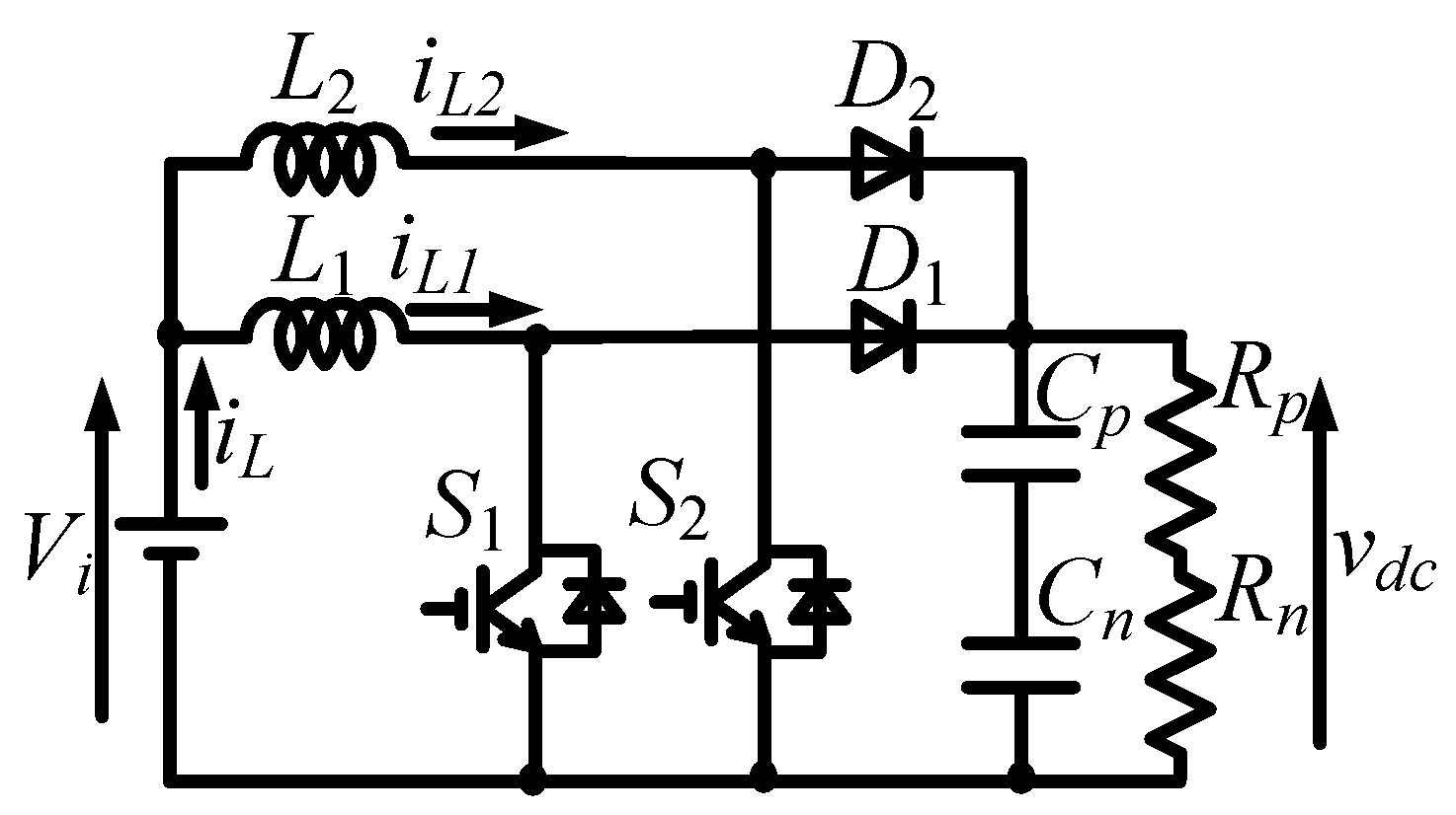
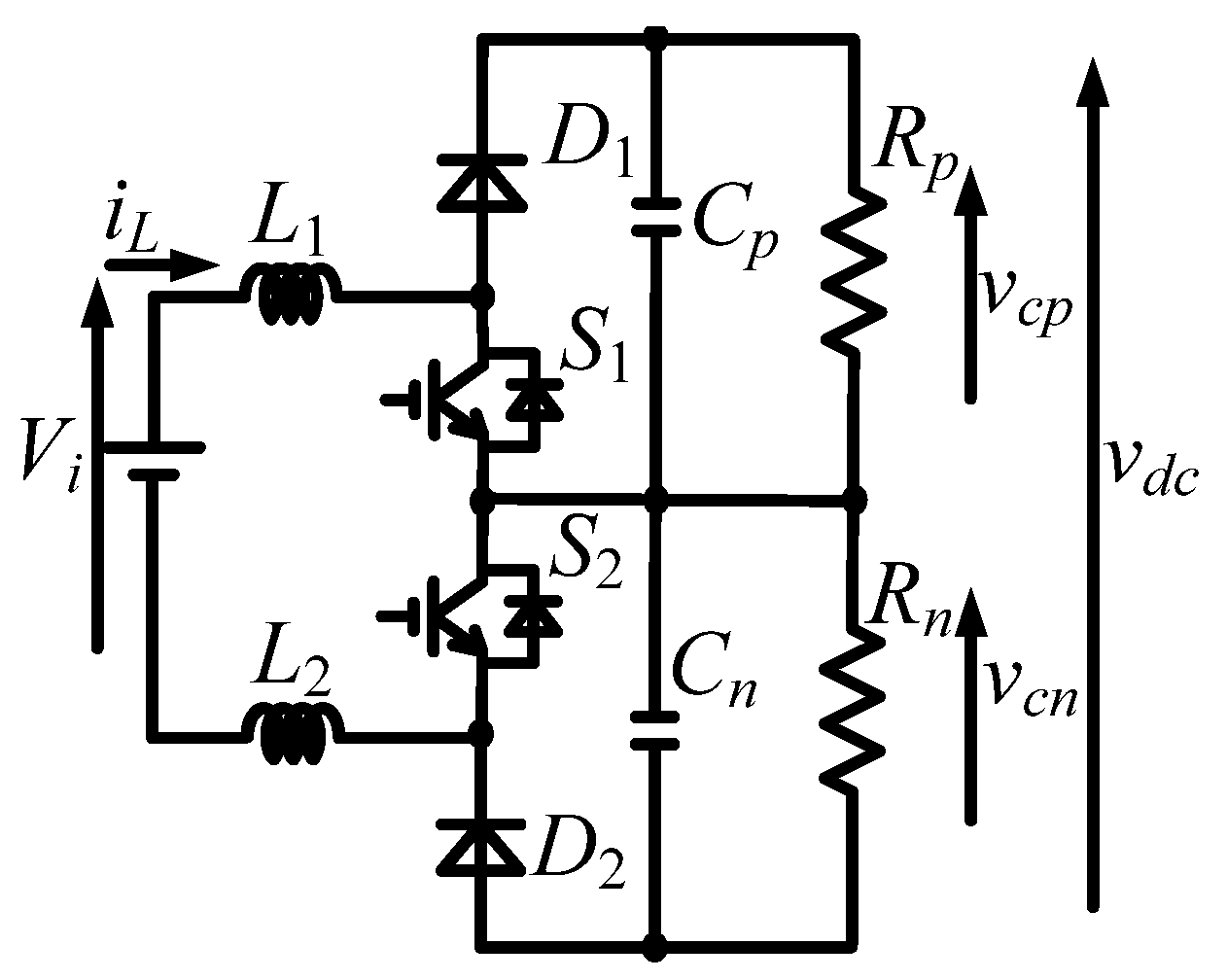
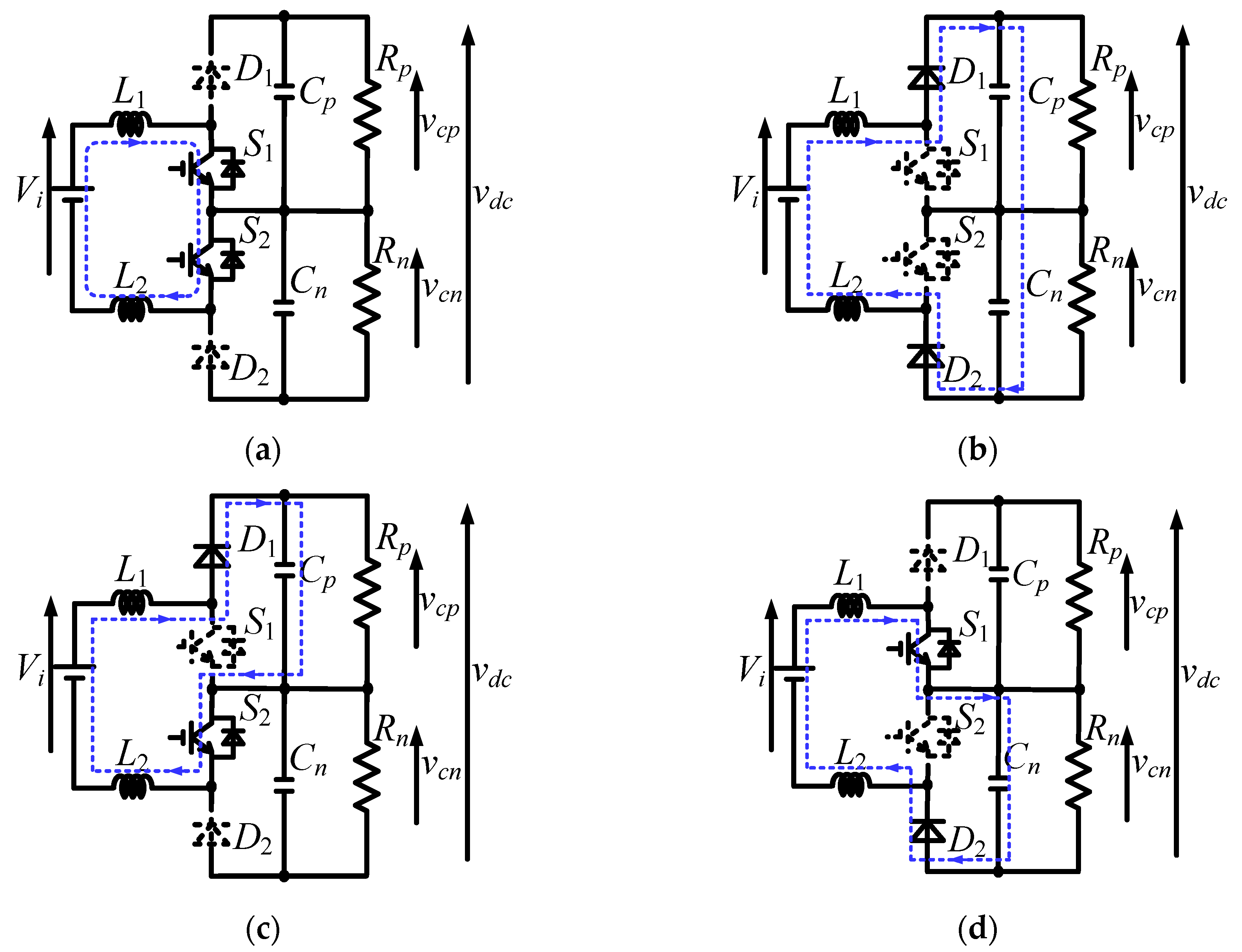
2. Circuit Configuration
In this chapter, the series and parallel circuits are presented and the switching mode analysis in the interleaved scheme is presented. It is assumed that a three-level inverter is connected as the load of the boost converter. However, a resistor is connected as the load because this paper focuses on the input current ripple and output voltage characteristics due to boost operation.
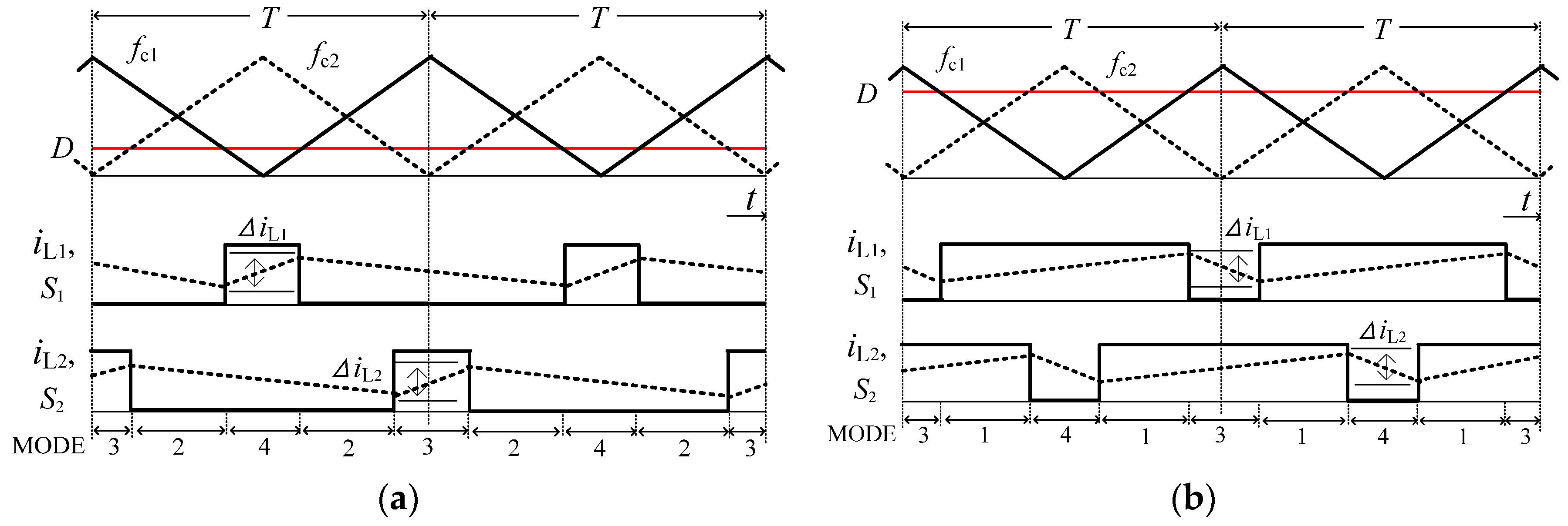
2.1. Interleaving Scheme
Figure 1 and Figure 2 show the parallel and series circuits, respectively. Figure 1 shows a configuration in which the boost converters are connected in parallel. Figure 2 shows a configuration in which the boost converters are connected in series. This paper proposes an interleaving method to generate the gate signals for series circuits. Figure 3 shows the principle of the interleaving method, where Dp and Dn are the duty ratios given to the switches (S1 and S2) in Figure 1 and Figure 2, respectively. Figure 3a shows the case where D ≤ 0.5 and Figure 3b shows the case where D > 0.5. As shown in Figure 3a, the controller modulates the command value using two carriers fc1 and fc2 with a phase difference of 180 degrees to generate the gate signals for the switches. Here, each switch, carrier, and duty ratio correspond to fc1 and Dp for S1, and fc2 and Dn for S2, respectively. Due to the interleaving method, the frequency of the input current ripple is twice the carrier frequency.
Figure 1.
Parallel circuit.
Figure 2.
Series circuit.
Figure 3.
Carriers and switching modes of interleaving method. (a) ; (b) .
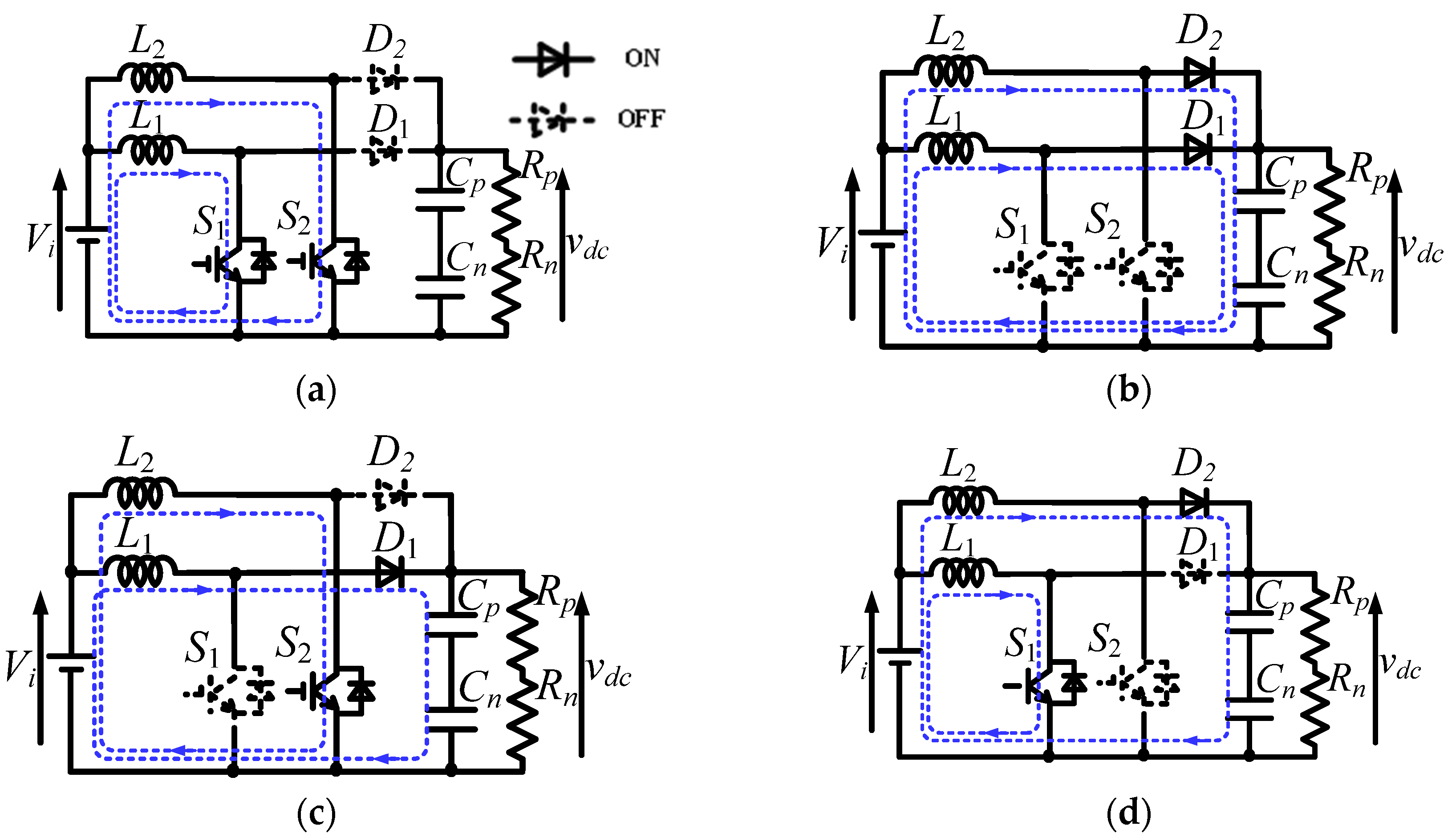
2.2. Switching Modes
In the two circuits, four modes appear depending on the magnitude of D. The switching modes of the parallel and series circuits are shown in Figure 4 and Figure 5, respectively. In both circuits, MODE1 in Figure 4a and Figure 5a is a mode in which both S1 and S2 are on, MODE2 in Figure 4b and Figure 5b is a mode in which both S1 and S2 are off, MODE3 in Figure 4c and Figure 5c is a mode in which S1 is off and S2 is on, and MODE4 in Figure 4d and Figure 5d is a mode in which S1 is on and S2 is off. For D > 0.5 in Figure 3b, magnetic energy is stored in both reactors with MODE 1 in Figure 4a and Figure 5a and boosted with MODE 3 in Figure 4c and Figure 5c and MODE 4 in Figure 4d and Figure 5d alternately. The upper and lower capacitor voltages (vcp, vcn) of the series circuit are controlled separately by charging the upper capacitor with MODE 3 in Figure 5c and the lower capacitor with MODE 4 in Figure 5d.
Figure 4.
Switching modes of parallel circuit. (a) MODE1; (b) MODE2; (c) MODE3; (d) MODE4.
Figure 5.
Switching modes of series circuit. (a) MODE1; (b) MODE2; (c) MODE3; (d) MODE4.
3. Input Current Ripple Analysis
This chapter derives a theory of the switching ripple ΔiL of the input current iL for both circuits. As the operating mode of the input current, this chapter assumes a current continuous mode. For simplicity of analysis, each phase of the parallel circuit and the upper and lower of the series circuit are symmetrical. Each inductance value and duty ratio of the two switches are also the same. In other words, this chapter is analyzed with L1 = L2 = L and Dp = Dn = D. This chapter also discusses the input current ripple considering the rated current of the reactor.
3.1. Input Current Ripple in Parallel Circuits
In a parallel circuit, each reactor is connected in parallel to the power supply, so the input current ripple ΔiL is the sum of each reactor current ripple ΔiL1 and ΔiL2. Figure 3a shows the gate signal and each reactor current iL1 and iL2 when D ≤ 0.5. When both S1 and S2 are off, each reactor current ripple ΔiL1 and ΔiL2 are as follows [7]:
where ΔiL1, ΔiL2 > 0 as defined in Figure 3 due to Vi < vdc.
Each reactor current has the same peak-to-peak value and a phase difference 180 degrees as shown in Figure 3a. The input current ripple ΔiL becomes their sum, and considering vdc = Vi/(1 − D), the current ripple becomes Equation (3).
Figure 3b shows the gate signal and each reactor current when D > 0.5. In this case, when both S1 and S2 are on, each reactor current ripple ΔiL1 and ΔiL2 are as in Equation (4).
The input current ripple ΔiL is expressed as Equation (5).
3.2. Input Current Ripple in Series Circuits
In a series circuit, each reactor is connected in series with the input power supply, so the reactor value is doubled and the input current ripple ΔiL is half that of one phase in a parallel circuit. In other words, the current ripple is half of Equation (1) when D ≤ 0.5. Moreover, when vdc = Vi/(1 − D) is taken into account, Equation (6) is obtained.
On the other hand, the current ripple for D > 0.5 is half of Equation (4).
Based on the above equations, if the inductance values of both the parallel circuit and the series circuit are equal, the input current ripple of the series circuit is one-quarter that of the parallel circuit. Next, the input current ripple is discussed considering the rated current of the reactor. Since the parallel circuit is connected in parallel, the rated current of the reactor is half of the input current. On the other hand, the series circuit is series connected, so the rated current of the reactor is the same as the input current. Therefore, the rated current of the reactor in a series circuit is twice that of a parallel circuit. The volume and weight of the reactor are approximately determined by the product of the inductance value and the square of the reactor current (LI2). If the inductance value of the series circuit is set to one-quarter of the parallel circuit, the input current ripple of the two circuits will be equal.
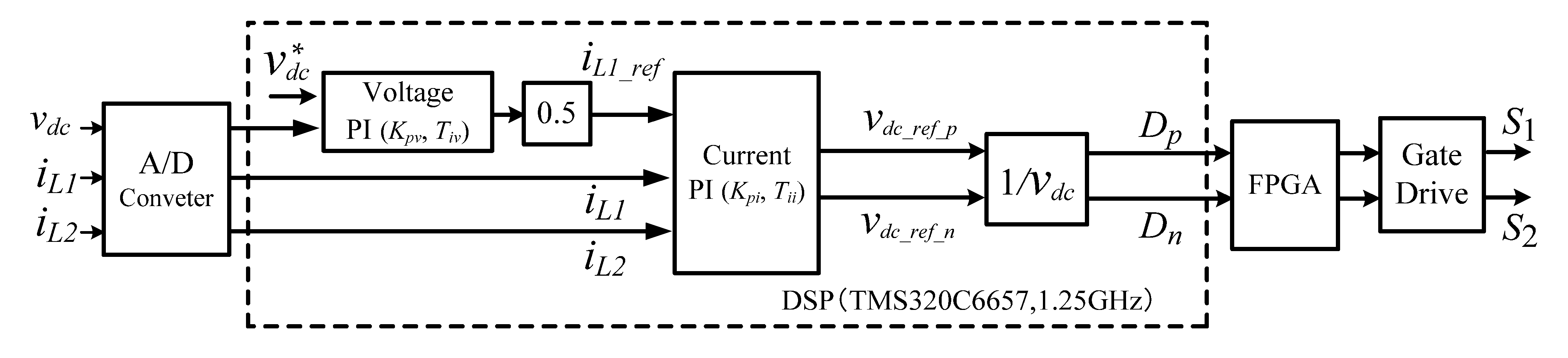
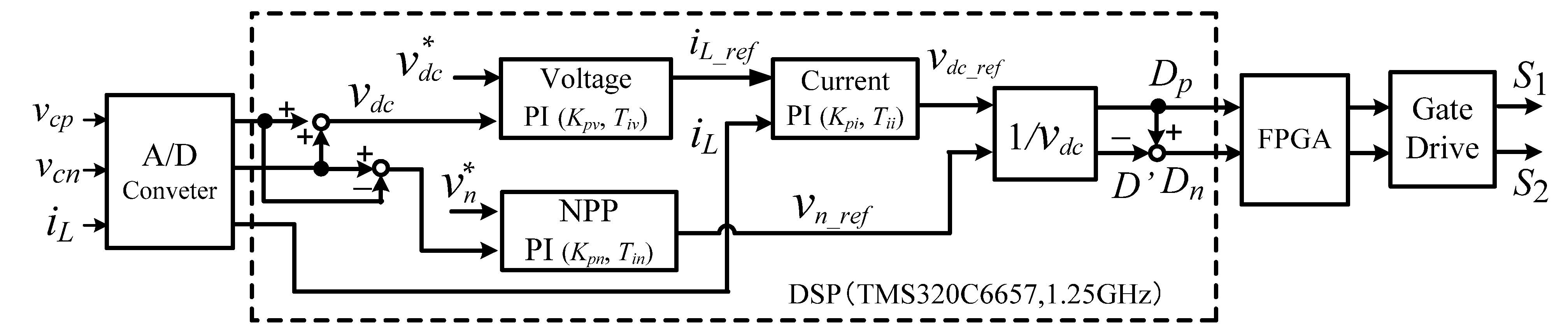
4. Output Voltage Control
This chapter describes the output voltage control method using PI control. After that, the output voltage control method using the optimal regulator (LQR) is described. There are two advantages of applying LQR to multilevel inverters. First, LQR allows a fast load response by using optimal control input. In Reference [8], it is demonstrated that the fast load response of the controller is capable of downsizing the smoothing capacitor. The series circuit is designed to be applied to a three-level inverter, which requires a larger smoothing capacitor than a two-level inverter in order to balance the neutral point potential in the DC link voltage. Therefore, LQR can contribute to the reduction in the smoothing capacitor capacity of the three-level inverter. Next, when the number of state variables increases by connecting a boost converter and a three-level inverter, LQR can collectively control the state variables of the extended system due to its excellent extendibility.
4.1. PI Control
Figure 6 and Figure 7 show the control block diagram of each boost converter circuit. In Figure 6, the reactor current (iL1, iL2) and output voltage (vdc) are obtained by sensors, and the deviation between the voltage command value and the actual voltage is input to the PI controller to obtain the input current command. The deviation between the current command value and the actual current is then input to the PI controller to calculate the duty ratio of the boost converter, which is modulated by a carrier wave to generate a gate signal. In Figure 7, the capacitor voltages (vcp, vcn) and reactor current (iL) are obtained by sensors, and the duty ratio is calculated as in Figure 6. The difference between Figure 6 and Figure 7 is that a control system for the neutral point potential (NPP) is added to control the balance between the upper and lower capacitor voltages. Neutral point potential vn is defined as the following equation:
Figure 6.
Configuration of parallel circuit with PI controller.
Figure 7.
Configuration of series circuit with PI controller.
The command value of the neutral point potential is set to vn* = 0. The current PI controller outputs vdc_ref so that Dp equals Dn when the neutral point potential is 0 V. The NPP PI controller outputs vn_ref according to the error of the neutral point potential from the command value to realize the balance control. Defining the difference between Dp and Dn as D’= Dp − Dn, the NPP PI controller corrects Dn with D’ when the neutral point potential varies.
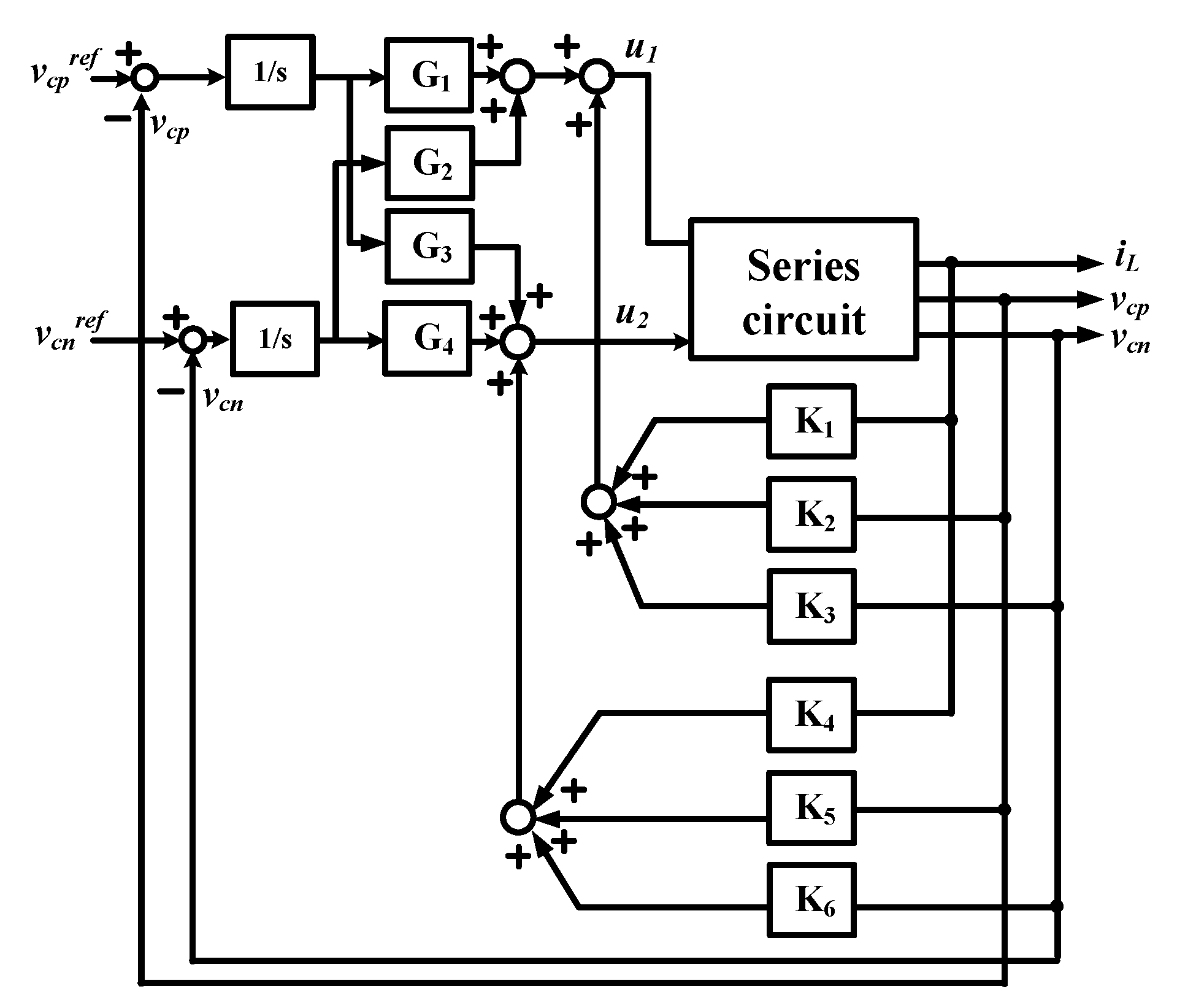
4.2. Output Voltage Control Using Optimal Regulator
The state equation in the current continuous mode of the series circuit shown in Figure 2 can be expressed by the following equation when the state averaging method is used, where the output time of each MODE is T1 = (Dp + Dn − 1) T for MODE1, T3 = (1 − Dp) T for MODE3, and T4 = (1 − Dn) T for MODE4, for D > 0.5 shown in Figure 3b.
where u(t)≔ Vi, = 1 − Dp, = 1 − Dn, C = Cp = Cn, R = Rp = Rn. From Equations (9)–(12), the state Equation (9) is a nonlinear system. In this paper, the state equation is designed to be linearized around the equilibrium point. The equilibrium point is set as x(t) = X, u(t) = U. Assuming that the variation in the equilibrium point is sufficiently slower than the carrier period, a small signal model is obtained as follows:
where , and the value of the equilibrium point is Equation (18).
Equation (13) is expanded as the servo system so that the controlled variables vcp and vcn are able to follow the step response. The state equation of the expanded system with additional state variable ω(t), which is the integral of the deviation e(t) between the controlled variables vcp, vcn and their reference values, is expressed as the following equations:
Figure 8 shows the configuration of the derived controller. The optimal regulator is used to determine the gains K and G in Equation (23). The evaluation function is expressed as the following:
where Q is the weight coefficient matrix for each state variable and R is the weight coefficient matrix for the magnitude of the control input.
Figure 8.
Configuration of series circuit with LQR.
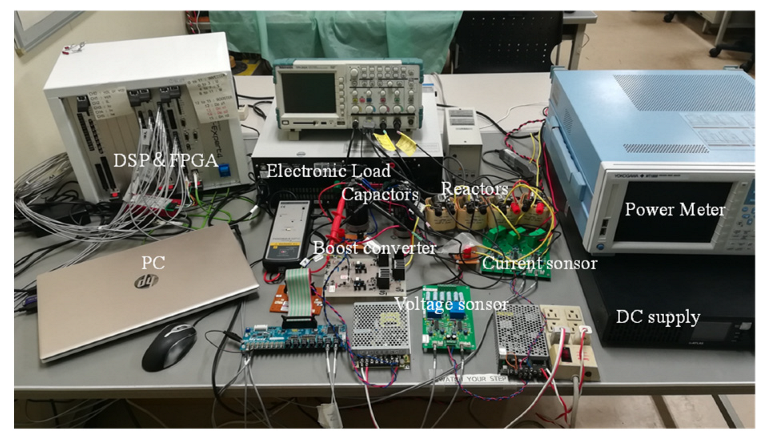
5. Experimental Verification
5.1. PI Control Design
Figure 9 shows the experimental setup. Table 1 shows the main circuit parameters. The parameters of the PI controller were designed using Bode diagrams and simulations. The response speed of the output voltage was set to be about 0.1 s for a 50 V step change in the command value. Simulation of the circuit shown in Figure 7 with the parameters shown in Table 1 resulted in a control bandwidth of 500 rad/s for the current control system, which allows the system to boost voltage stably. The control bandwidth of the voltage control system is 1/10 of that of the current control system, and the control bandwidth of the neutral point potential PI control is less than 1/2 of that of the voltage control system. Table 2 shows the control parameters.
Figure 9.
Experimental setup.
Table 1.
Circuit conditions.
Table 2.
Parameters of PI controllers.
5.2. Optimal Regulator Design
In this paper, the weight coefficients in Equation (24), which are necessary to calculate the gain of LQR, are designed through simulations. The output voltage response is set to be about 0.1 s as well as that of PI control, and the weight coefficient matrices Q and R of the LQR are set as Q = diag [q1, q2, q3, q4, q5] and R = diag [r1, r2], in which diag denotes the diagonal matrix. Each coefficient corresponds to q1:iL, q2:vcp, q3:vcn, q4:Δvcp, q5:Δvcn, r1:, r2:.
Figure 10 shows the simulated results when the weights are changed. Here, the weight coefficients for the inputs were set to R = diag [1, 1]. Comparing Figure 10a,b, it can be seen that the larger the weight on the deviation, the faster the response. Comparing Figure 10c,d, it can be seen that the response can be made faster by increasing the weight of Δvcn. Simulated results show that the desired response can be obtained when Figure 10e is used. For gain calculation, the “Arimoto-Potter method” is used. Table 3 shows the gains designed.
Figure 10.
Simulated results for weight coefficients design. (a) Q = diag([1,1,1,1,1]); (b) Q = diag([1,1,1,100,100]); (c) Q = diag([5,5,5,100,100]); (d) Q = diag([5,5,5,100,1000]); (e) Q = diag([5,5,2,100,1000]); (f) Q = diag([5,5,10,100,1000]).
Table 3.
Parameters of LQR for Q = diag [5,5,2,100,1000], R = diag [1,1].
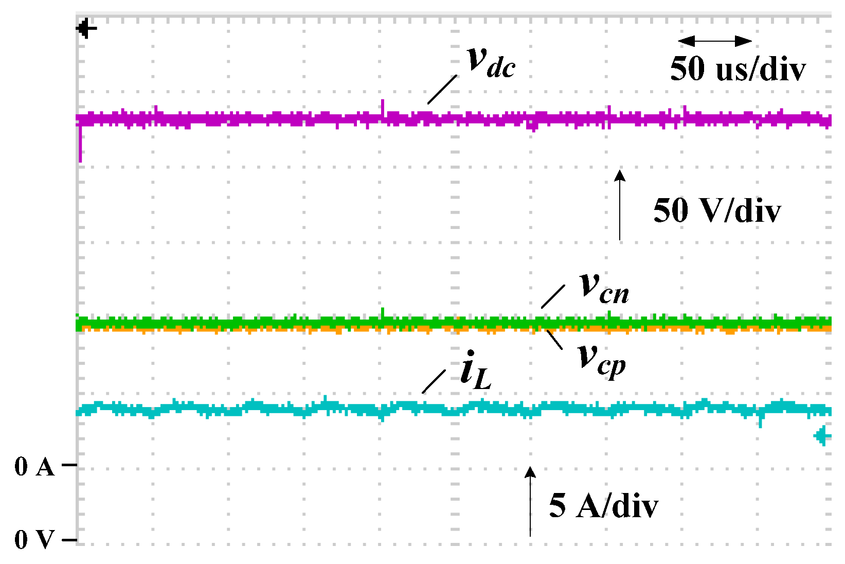
5.3. Boost Operation and Neutral Point Potential Control Characteristics
Figure 11 shows the experimental results when the proposed LQR is used in the circuit shown in Figure 2. The output voltage command value is 280 V and the neutral point potential command value is 0 V. The load resistance is 200 Ω. Figure 11 shows that both the output voltage and neutral point potential follow the command value well.
Figure 11.
Steady state characteristics of series circuit.
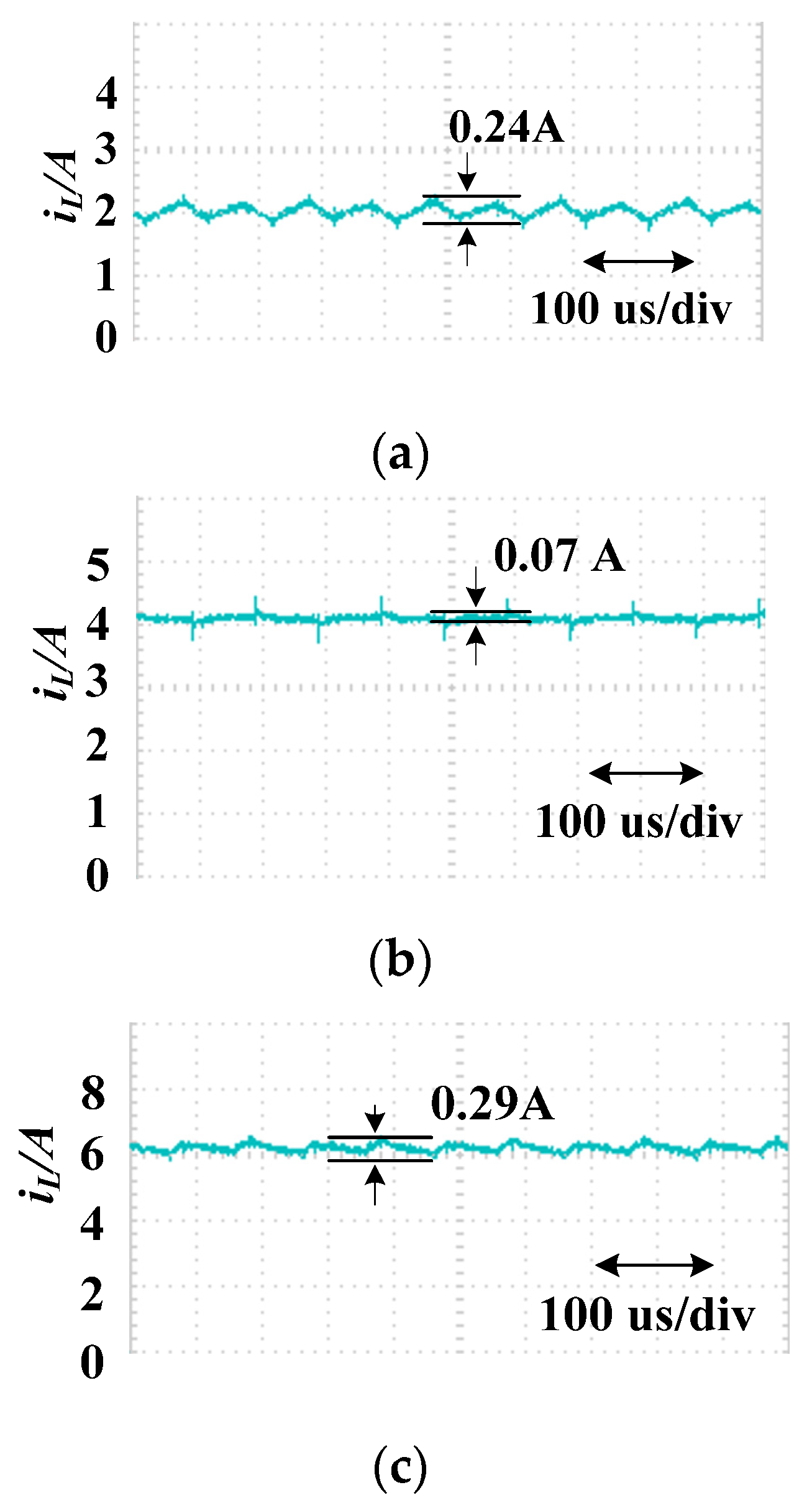
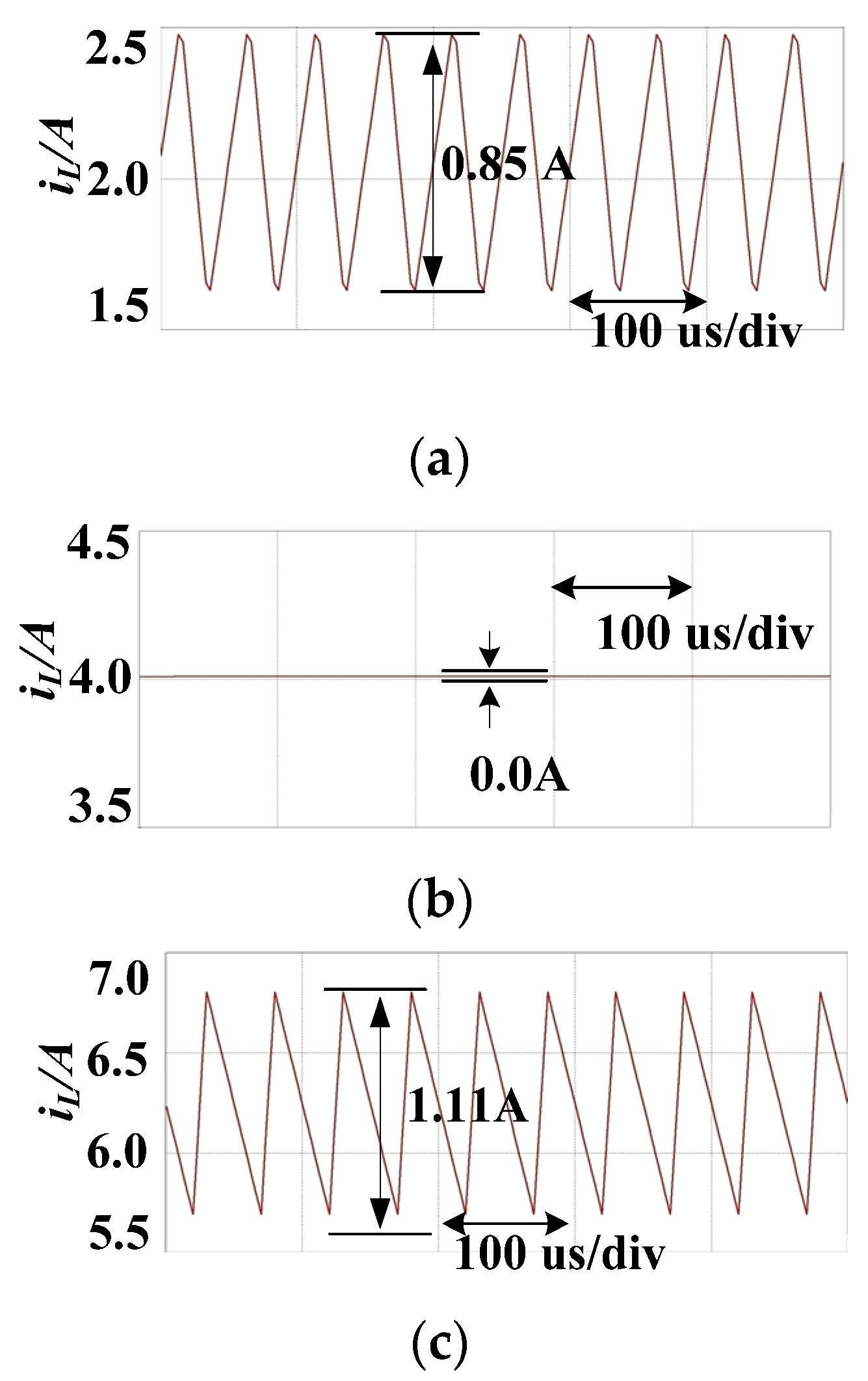
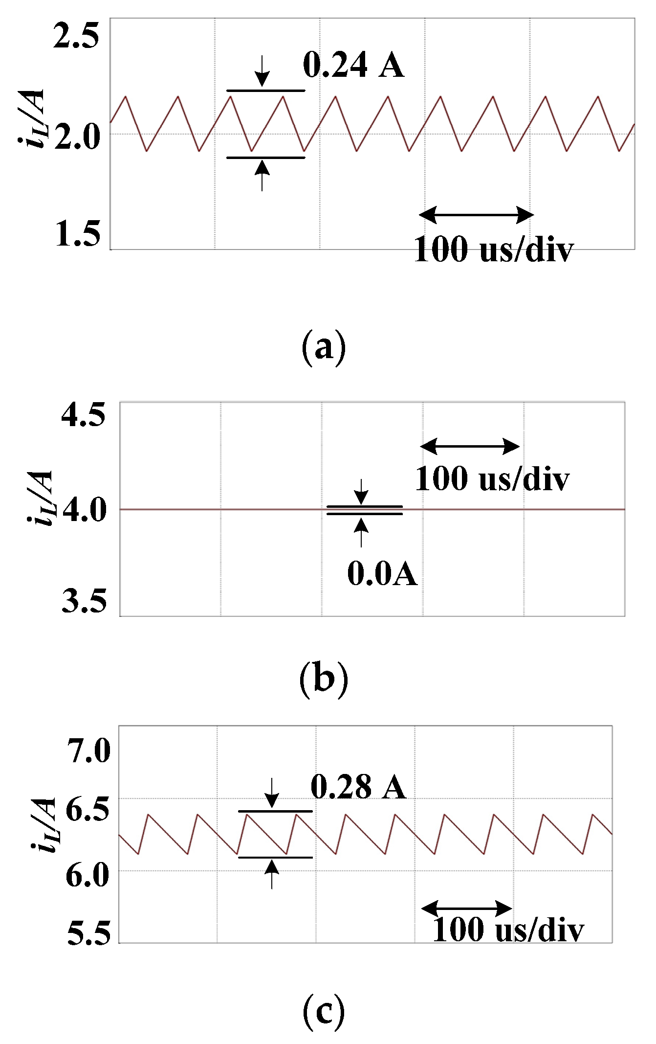
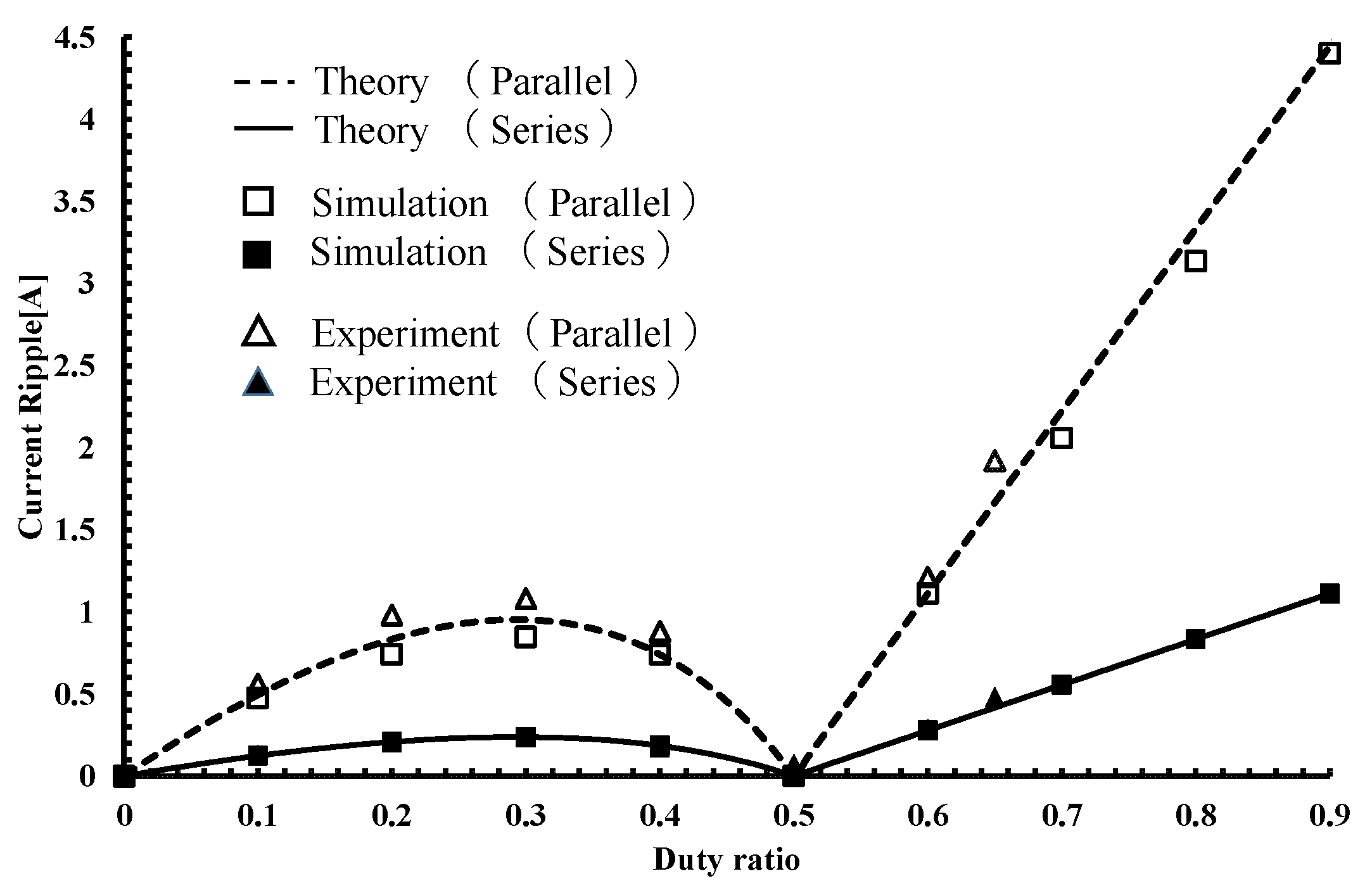
5.4. Input Current Ripple Characteristics
Figure 12 and Figure 13 show the experimental results of the input current ripple. The load resistance is 100 Ω (Rp = Rn = 50 Ω). Figure 12 and Figure 13 show the input current ripple of the parallel and series circuits, respectively. These are the results obtained by open-loop control for the duty ratios of 0.3, 0.5, and 0.6, respectively. When D = 0.3 and 0.6, the input current ripple of the series circuit is approximately one-quarter that of the parallel circuit. Figure 14 and Figure 15 show the simulated results of the input current for the same load condition. It can be seen that the simulation and experimental results are in good agreement for D = 0.5 and D = 0.6. Comparing Figure 12a and Figure 14a in the case of D = 0.3, there is a difference between them. It can be mainly attributed to the effect of the turn on and turn off time in the experiment. Figure 16 shows a comparison of the theoretical, simulated, and experimental results for the input current ripple. In the experimental results, the duty ratio was set to a maximum of 0.65 due to the limitation of the rated voltage of the experiment equipment. As shown in Figure 16, the input current ripple of the series circuit is one-quarter that of the parallel circuit.
Figure 12.
Experimental results of input current ripple characteristics of parallel circuit. (a) D = 0.3; (b) D = 0.5; (c) D = 0.6.
Figure 13.
Experimental results of input current ripple characteristics of series circuit. (a) D = 0.3; (b) D = 0.5; (c) D = 0.6.
Figure 14.
Simulated results of input current ripple characteristics of parallel circuit. (a) D=0.3; (b) D = 0.5; (c) D = 0.6.
Figure 15.
Simulated results of input current ripple characteristics of series circuit. (a) D = 0.3; (b) D = 0.5; (c) D = 0.6.
Figure 16.
Input current ripple characteristics for duty ratio.
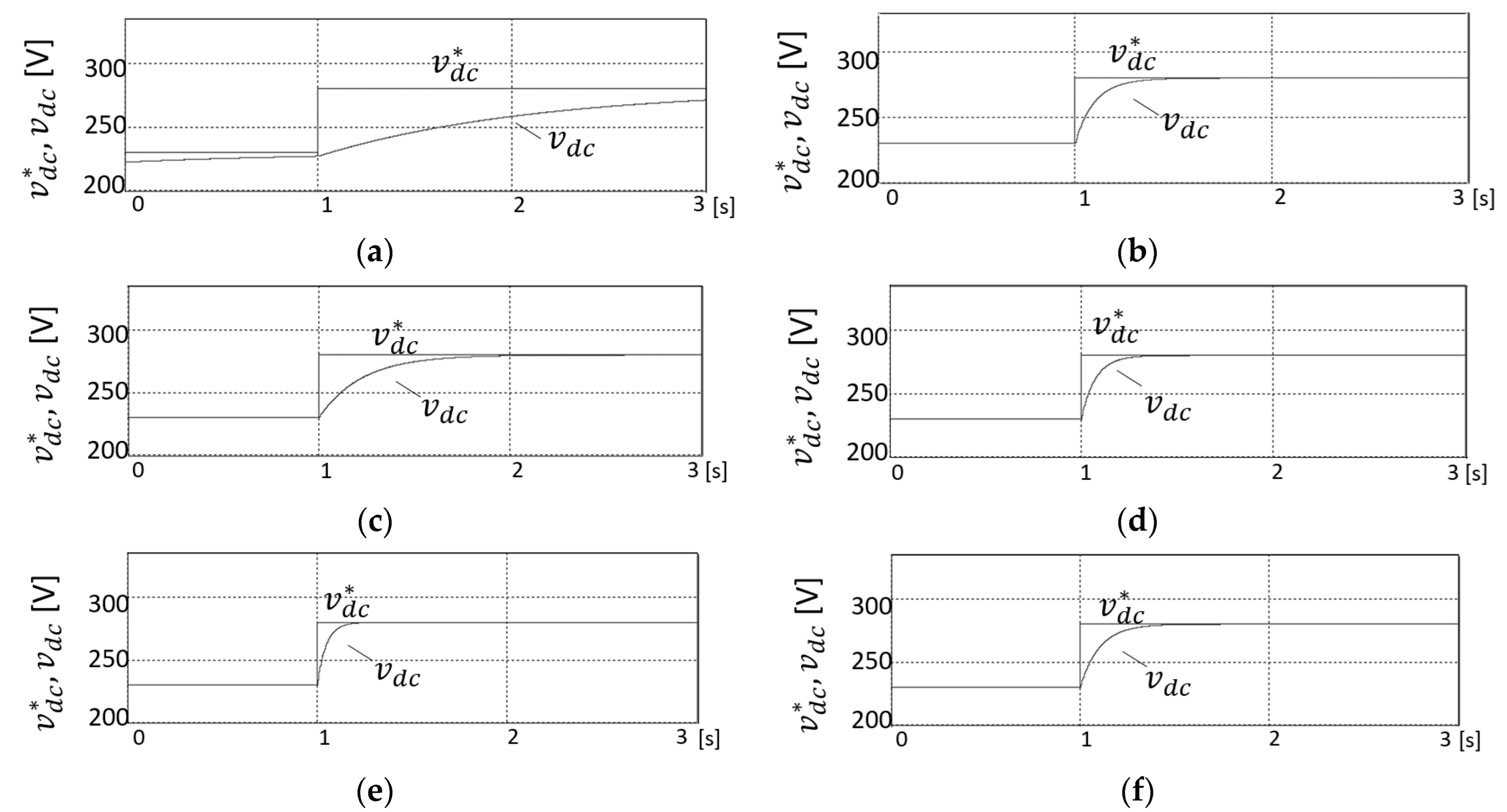
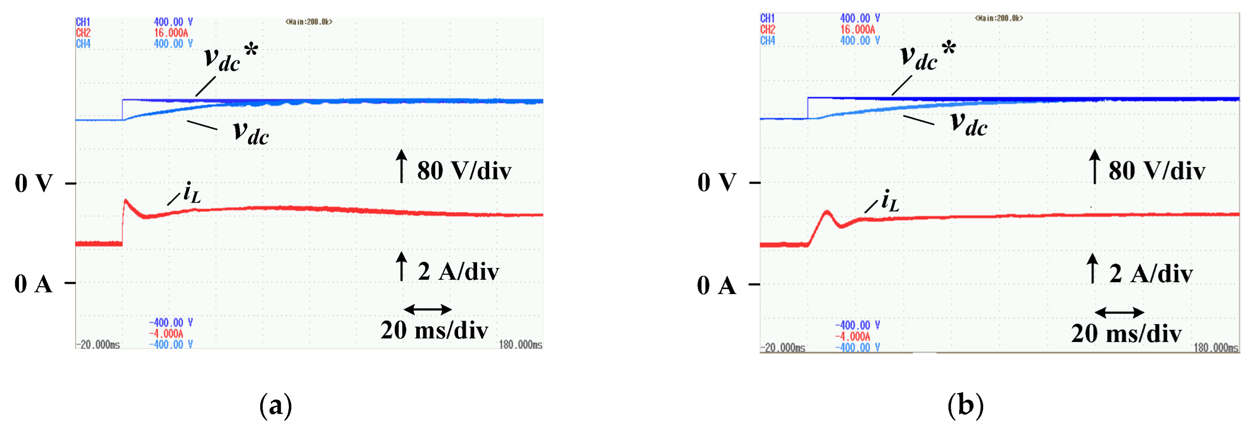
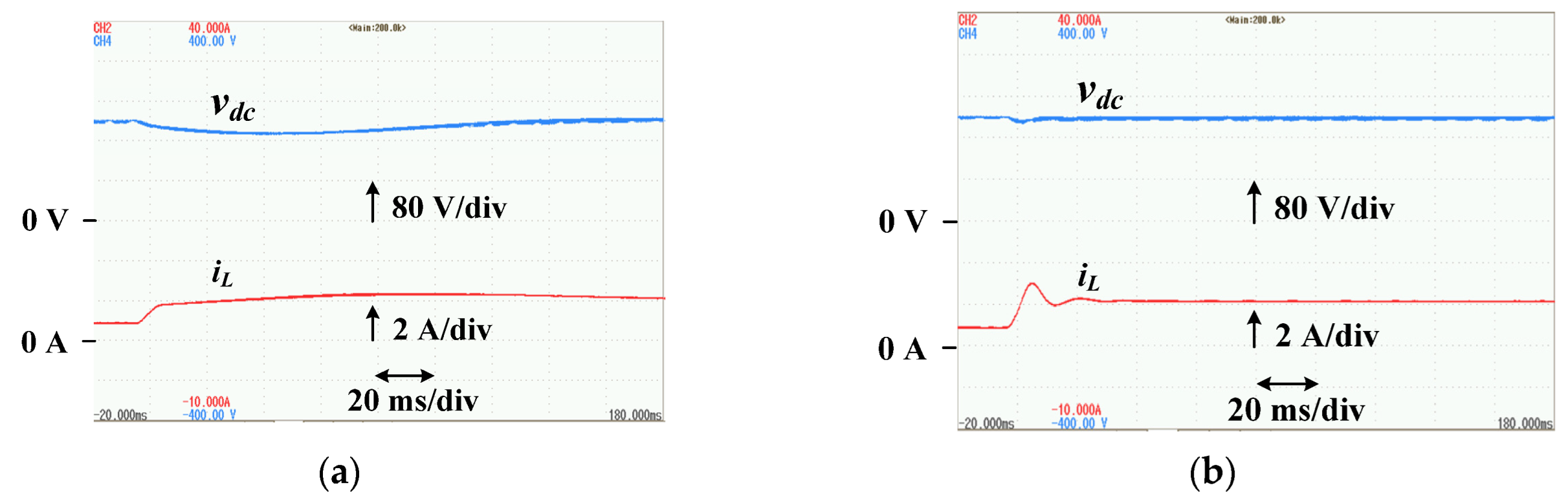
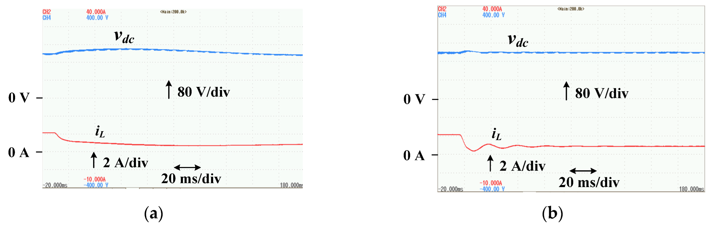
5.5. Output Voltage Response Characteristics
Figure 17 shows the response of the output voltage and input current when the voltage command is changed in steps from 150 V to 200 V. Both the output voltages in cases Figure 17a,b respond in about 100 ms, which is the desired response. Figure 18 shows the response when the load is changed from 200 W to 500 W. In case Figure 18a, the output voltage drops by a maximum of about 25 V and fluctuates for 140 ms, while in case Figure 18b, the output voltage drops by up to 8 V but recovers in about 10 ms. Figure 19 shows the response when the load is varied from 500 W to 200 W. In case Figure 19a, the output voltage rises up to about 20 V and fluctuates over 140 ms. In case Figure 19b, the output voltage rises by a maximum of about 8 V but recovers in about 10 ms. These results show that the response of the proposed LQR to load fluctuations is superior to that of PI control.
Figure 17.
Step response (150 V to 200 V). (a) PI control; (b) LQR.
Figure 18.
Load variation (200 W to 500 W). (a) PI control; (b) LQR.
Figure 19.
Load variation (500 W to 200 W). (a) PI control; (b) LQR.
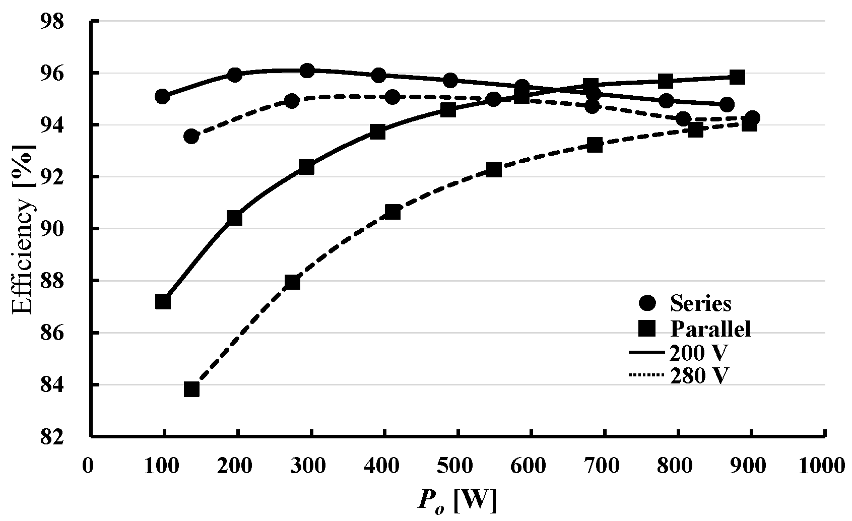
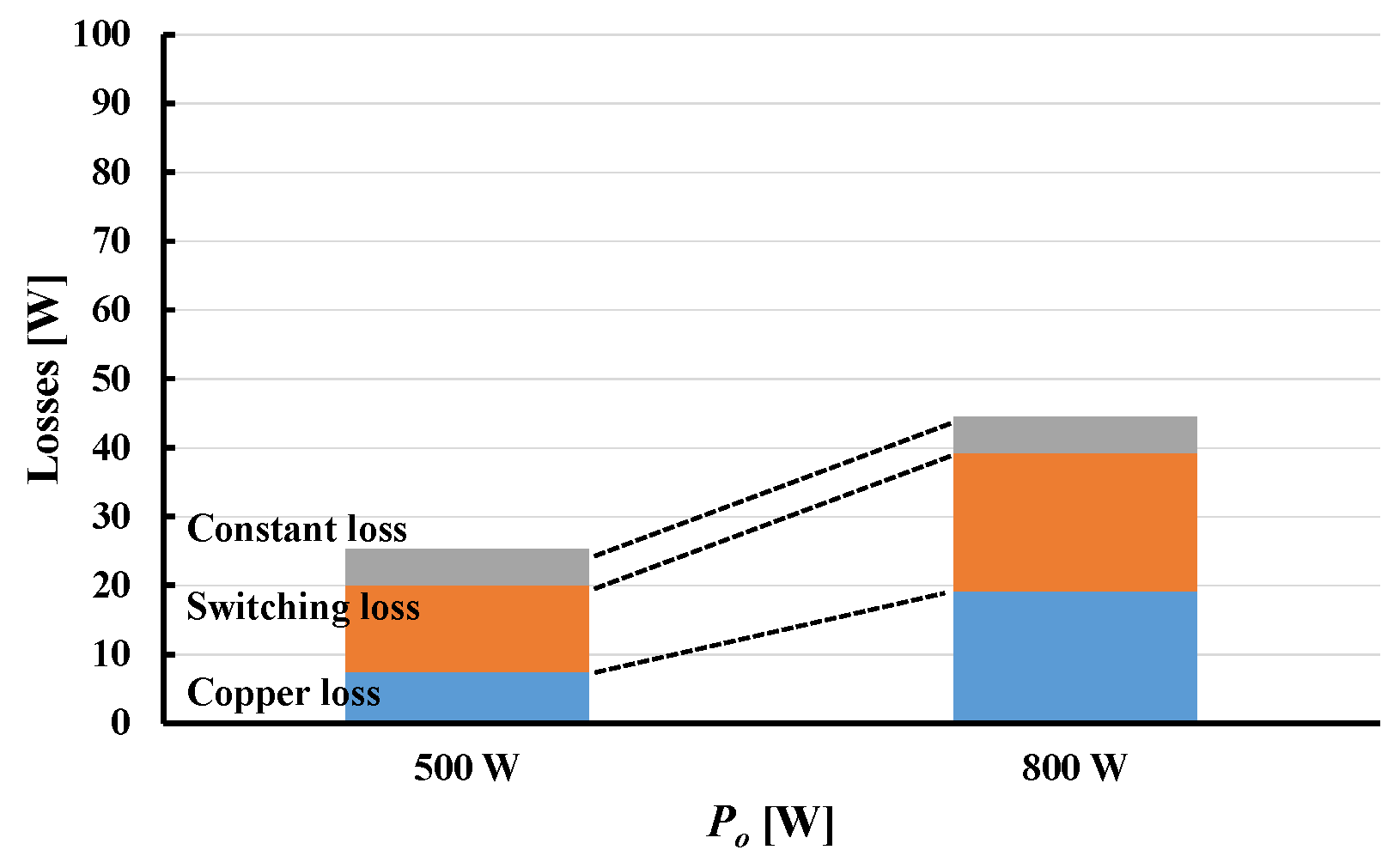
5.6. Efficiency Characteristics
Figure 20 shows the characteristics of conversion efficiency versus output voltage. When the load power is 500 W, the parallel circuit has high efficiency when the output voltage is 160 V (duty ratio 0.38) or lower. At higher output voltages, the series circuit is highly efficient. When the load power is 800 W, the series circuit is higher in efficiency when the output voltage is 240 V (duty ratio 0.58) or higher. Thus, the conversion efficiency of the series circuit is higher than that of the parallel circuit at light loads and high output voltages.
Figure 20.
Efficiency characteristics for output voltage.
Figure 21 shows a comparison of the efficiency with respect to the load. As for 280 V, the efficiency of the series circuit is higher than that of the parallel circuit over the entire range. As for 200 V, the efficiency of the series circuit is higher below 630 W. When the load power is 300 W, the efficiency of the series circuit is 96%, compared to 92% for the parallel circuit. These results show that the series circuit has an advantage in conversion efficiency in the light load and high voltage range. Figure 22 and Figure 23 show the loss separation results for the parallel and series circuits. When the output power is 500 W, the switching losses are 32.4 W and 12.5 W, and the iron losses are 19.5 W and 5.22 W, respectively. The iron loss of the series circuit is about one-quarter that of the parallel circuit, and the switching loss is about one-third. The reason of that is related to the input current ripple ∆iL described in Section 5.4. The difference between the input current ripple ∆iL of the two circuits becomes large when the duty ratio is greater than 0.5. The input current ripple ∆iL of the parallel circuit is larger than that of the series circuit. Therefore, as shown in Figure 20, the efficiency of the parallel circuit decreases largely due to increased switching losses.
Figure 21.
Efficiency characteristics for output power.
Figure 22.
Loss comparison of parallel circuit when output voltage is 280 V.
Figure 23.
Loss comparison of series circuit when output voltage is 280 V.
6. Conclusions
In this paper, an interleaving scheme for a series connected boost converter was proposed for application to a three-level inverter. The effectiveness of the proposed interleaving scheme is clarified by comparing the input current ripple characteristics with those of the parallel-connection-type interleaving scheme. The conclusions obtained in this paper are as follows:
- The series circuit is capable of both boosting and neutral potential control by means of a boost converter connected in a dependent manner, and is effective for use in a three-level inverter.
- A theoretical analysis of the input current ripple of the series circuit was performed. The validity of the analysis was demonstrated by experiments and simulations using an experimental apparatus with an output voltage of 280 V.
- When the inductances of the series circuit and the parallel circuit are equal, the input current ripple of the series circuit is one-quarter that of the parallel circuit.
- When the inductance of the series circuit is one-quarter of the parallel circuit and the volume and weight of both circuits are equal, the input current ripple of the two circuits are equal.
- As an output voltage control method for the series circuit, a control method using an optimal regulator was proposed, and a design method using the state averaging method is presented. The proposed optimal regulator has a better load regulation response than the general PI control method, suggesting that it is effective in downsizing the smoothing capacitor.
- The series circuit has higher conversion efficiency in the light load, high voltage region than the parallel circuit, and is suitable for operation in this region.
Author Contributions
Conceptualization, R.C.; methodology, R.C., E.S. and T.S.; software, R.C. and E.S.; validation, E.S. and R.S.; formal analysis, E.S. and R.S.; investigation, E.S., H.H. and R.M.K.; writing—review and editing, E.S., H.H. and R.M.K.; supervision, R.M.K.; project administration, E.S.; funding acquisition, E.S. and H.H. All authors have read and agreed to the published version of the manuscript.
Funding
This work was supported by JSPS KAKENHI Grant Number JP21K04038.
Institutional Review Board Statement
Not applicable.
Informed Consent Statement
Not applicable.
Data Availability Statement
Not applicable.
Conflicts of Interest
The authors declare no conflict of interest.
References
- Mizutani, M.; Tachibana, T.; Morimoto, M.; Akatsu, K.; Hoshi, N. Electric Drive Technologies Contributing to Low-Fuel-Consumption Vehicles. IEEJ Trans. Ind. Appl. 2015, 135, 884–891. (In Japanese) [Google Scholar] [CrossRef]
- Imai, K.; Kawamura, A.; Kinoshita, S.; Ashikaga, T.; Yokoe, K.; Asano, M. Electric Vehicle Related Technologies. Present Technologies and Future Trend on Power Electronics for Electric Vehicle. IEEJ Trans. Ind. Appl. 1996, 116, 223–244. (In Japanese) [Google Scholar] [CrossRef][Green Version]
- Nagai, M.; Wang, Y. Motion Control of Electric Vehicles by Distribution Control of Traction Forces. IEEJ Trans. Ind. Appl. 1996, 116, 279–284. (In Japanese) [Google Scholar] [CrossRef][Green Version]
- Heo, J.; Kondo, K. Design Method Considering the Frequency Band of the Disturbance in the DC Link Voltage Control System of Hybrid Electric Vehicle Driving Systems. IEEJ Trans. Ind. Appl. 2019, 139, 699–707. (In Japanese) [Google Scholar] [CrossRef]
- Marchesoni, M.; Vacca, C. New DC-DC Converter for Energy Storage System Interfacing in Fuel Cell Hybrid Electric Vehicles. IEEE Trans. PE. 2007, 22, 301–308. [Google Scholar] [CrossRef]
- Yamamoto, K.; Imakiire, A.; Iimori, K. PWM Inverter with Voltage Boosters with Regenerating Capability Augmented by Electric Double-Layer Capacitor. IEEJ Trans. Ind. Appl. 2011, 131, 671–678. (In Japanese) [Google Scholar] [CrossRef]
- Toru, A.; Haga, H.; Kondo, S. Comparison between Phase Number and Operation Mode of Multiphase Boost Chopper for Reducing Input Current Ripple. IEEJ Trans. Ind. Appl. 2012, 132, 250–257. (In Japanese) [Google Scholar] [CrossRef]
- Okuda, T.; Urakabe, T.; Tsunoda, Y.; Kikunaga, T.; Iwata, A. Ripple Current Reduction in DC Link Capacitor by Harmonic Control of DC/DC Converter and PWM Inverter. IEEJ Trans. Ind. Appl. 2009, 129, 144–149. (In Japanese) [Google Scholar] [CrossRef]
- Takei, D.; Fujimoto, H.; Hori, Y. Load Current Feedforward Control of Boost Converter for Downsizing the Output Filter Capacitor. IEEJ Trans. Ind. Appl. 2015, 135, 457–466. (In Japanese) [Google Scholar] [CrossRef]
- Sato, D.; Itoh, J. Improvement of the Electric Energy Consumption of Permanent Magnet Synchronous Motor Drive System Using Three-level Inverter. IEEJ Trans. Ind. Appl. 2015, 135, 632–640. (In Japanese) [Google Scholar] [CrossRef]
- Schweizer, M.; Kolar, W.J. Design and Implementation of a Highly Efficient Three-Level T-Type Converter for Low-Voltage Applications. IEEE Trans. PE. 2013, 28, 899–907. [Google Scholar] [CrossRef]
- Ogasawara, S.; Sawada, T.; Akagi, H. Analysis of the Neutral Point Potential Variation of Neutral-Point-Clamped Voltage Source PWM Inverters. IEEJ Trans. Ind. Appl. 1993, 113, 41–48. (In Japanese) [Google Scholar] [CrossRef][Green Version]
- Sakasegawa, E.; Shinohara, K. Compensation for Neutral Point Potential in Three Level Inverter by using Motor Currents. In Proceedings of the 15th International Conference on Electrical Machines, ICEM2002, Brugge, Belgium, 25–28 August 2002. [Google Scholar]
- Zaragoza, J.; Pou, J.; Ceballos, S.; Robles, E.; Ibanez, P.; Villate, L.J. A Comprehensive Study of a Hybrid Modulation Technique for the Neutral-Point-Clamped Converter. IEEE Trans. IE. 2009, 56, 294–303. [Google Scholar] [CrossRef]
- Yaramasu, V.; Wu, B.; Alepuz, S.; Kouro, S. Predictive Control for Low-Voltage Ride-Through Enhancement of Three-Level-Boost and NPC-Converter-Based PMSG Wind Turbine. IEEE Trans. IE. 2014, 61, 6832–6843. [Google Scholar] [CrossRef]
- Sakasegawa, E.; Matsumoto, T.; Tokunaga, K.; Haga, H. Control Method to Reduce Current Ripple of Boost Chopper Suitable for NPC Inverter. In Proceedings of the IEEE 9th IPEMC 2020 ECCE Asia, Nanjing, China, 29 November–2 December 2020; pp. 2467–2642. [Google Scholar]
Disclaimer/Publisher’s Note: The statements, opinions and data contained in all publications are solely those of the individual author(s) and contributor(s) and not of MDPI and/or the editor(s). MDPI and/or the editor(s) disclaim responsibility for any injury to people or property resulting from any ideas, methods, instructions or products referred to in the content. |
© 2022 by the authors. Licensee MDPI, Basel, Switzerland. This article is an open access article distributed under the terms and conditions of the Creative Commons Attribution (CC BY) license (https://creativecommons.org/licenses/by/4.0/).