

Photonic Crystal Flip-Flops: Recent Developments in All Optical Memory Components

Abstract
:1. Introduction
2. Fundamental Properties of Photonic Crystals in All-Optical Memory
3. Fundamental Properties of All-Optical Flip-Flops
3.1. Operating Wavelength
3.2. Switching Speed
3.3. Contrast Ratio
4. Different Flip-Flop Variations and Methods of Design
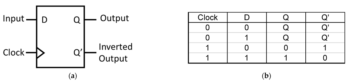
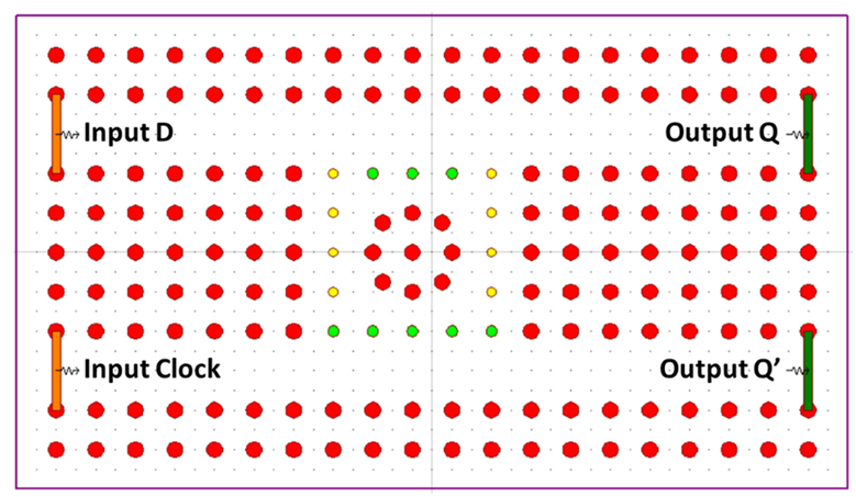
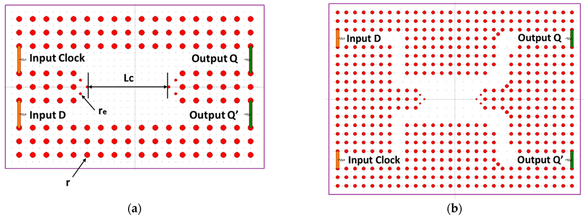
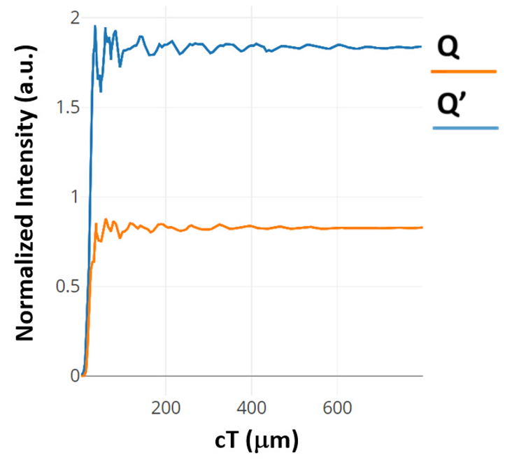
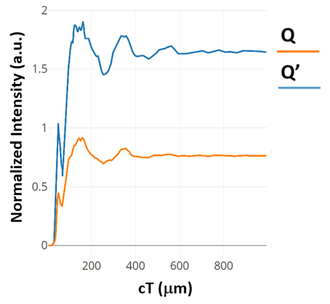
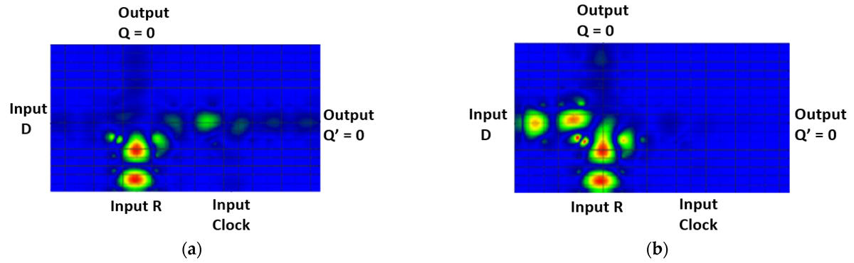
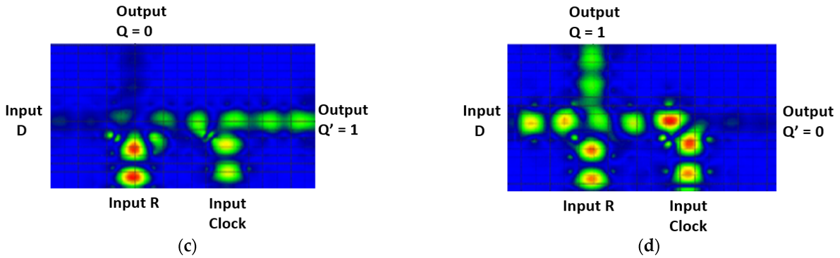
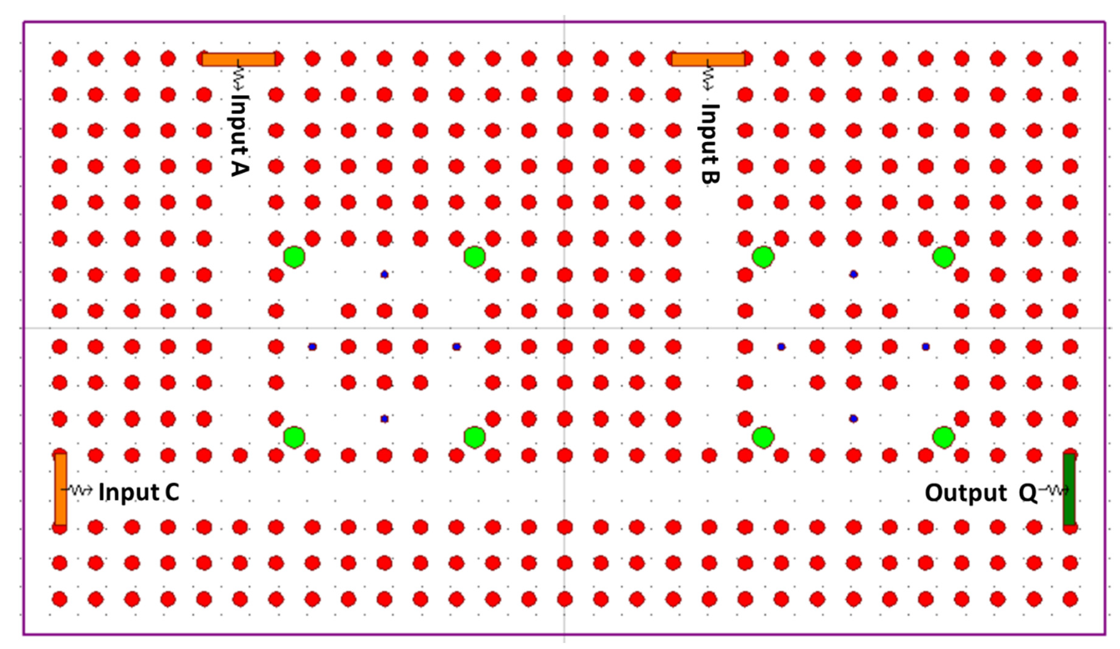
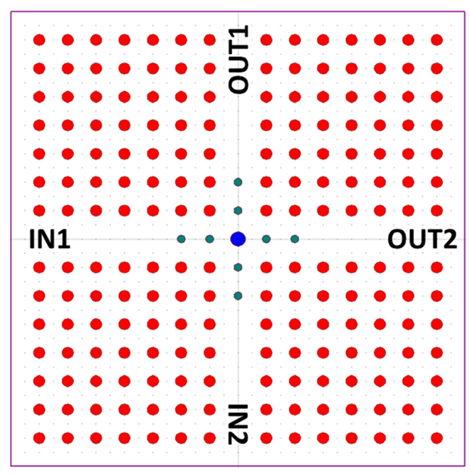
4.1. The D Flip-Flop
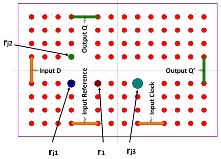
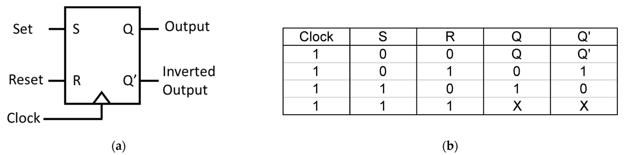
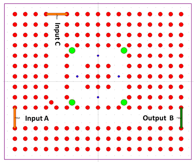
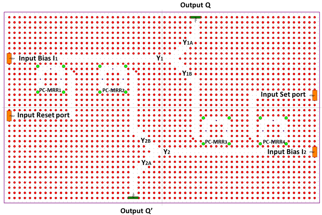
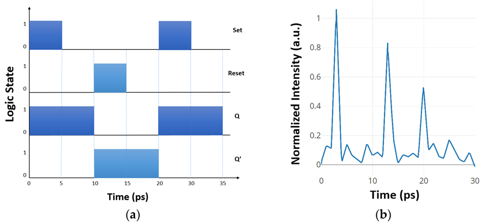
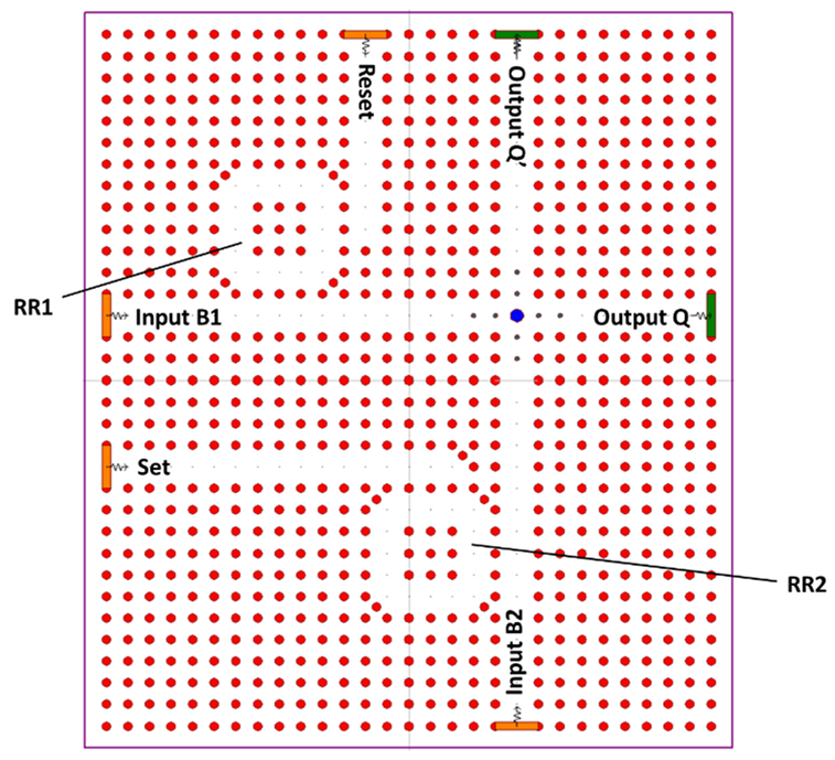
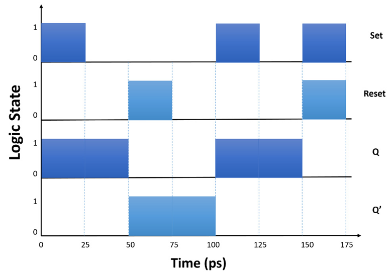
4.2. The SR Flip-Flop
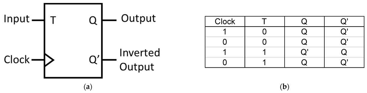
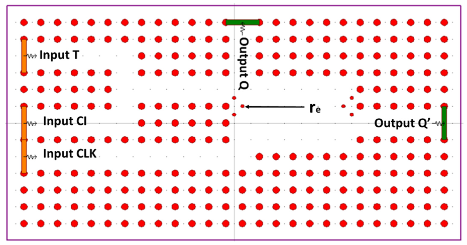
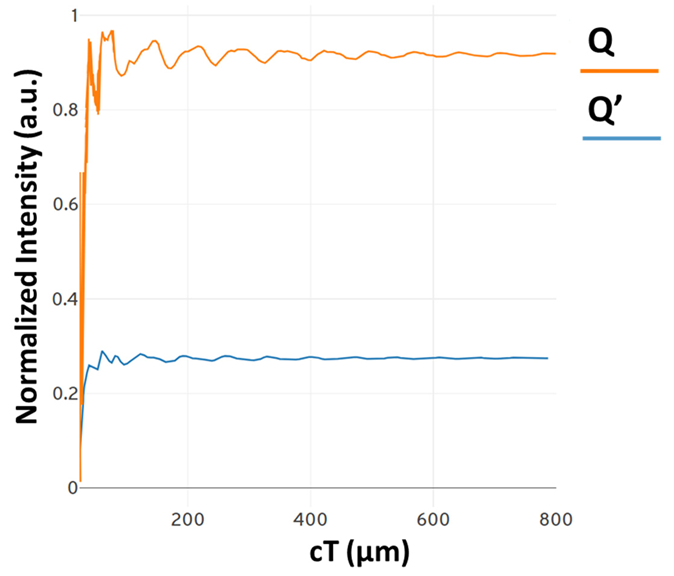
4.3. The T Flip-Flop
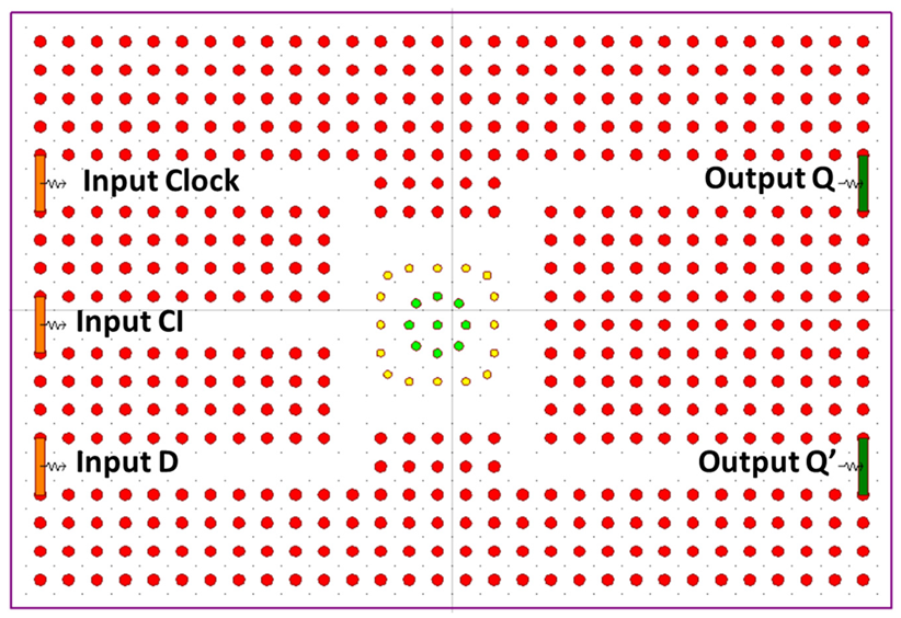
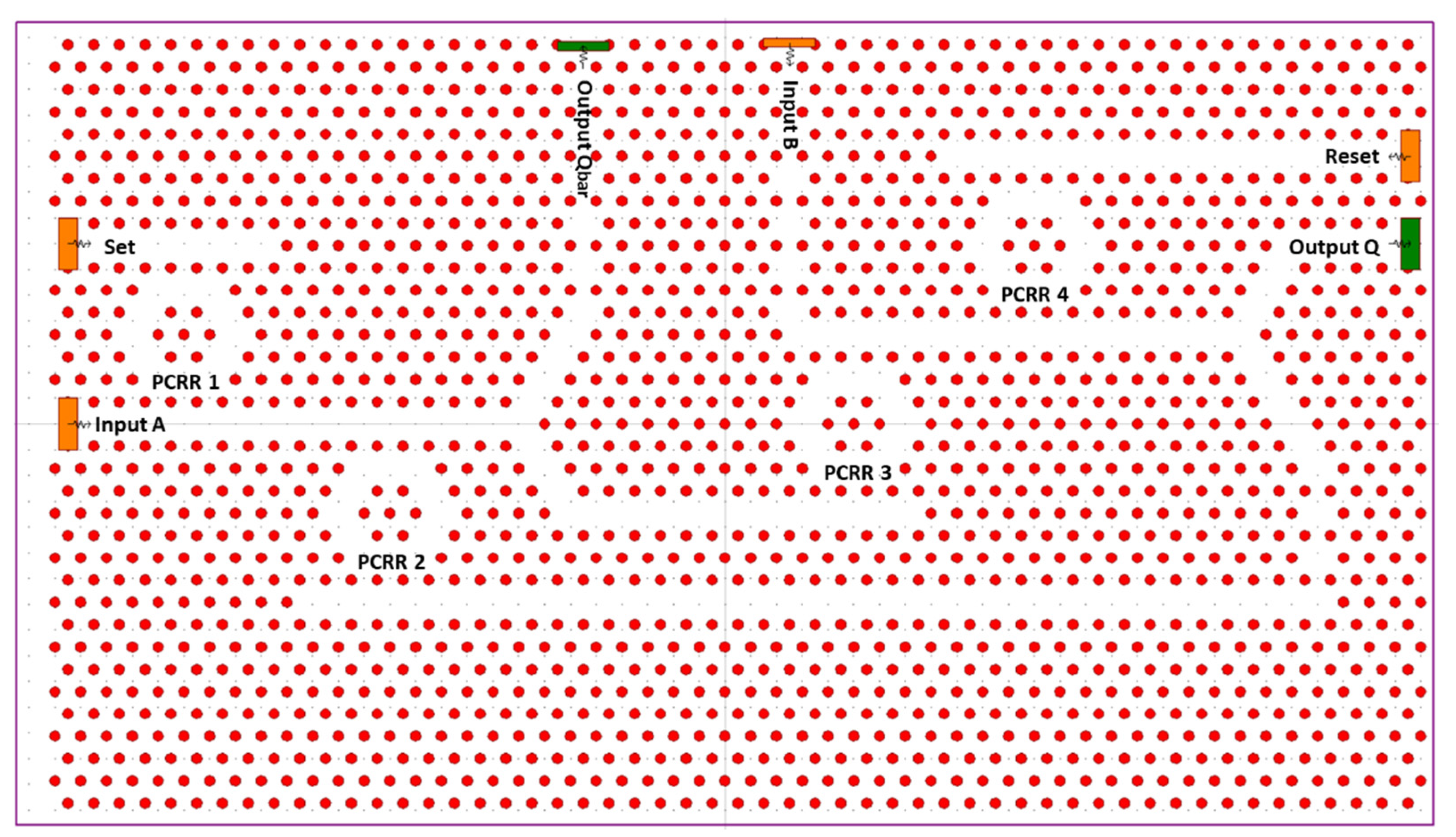
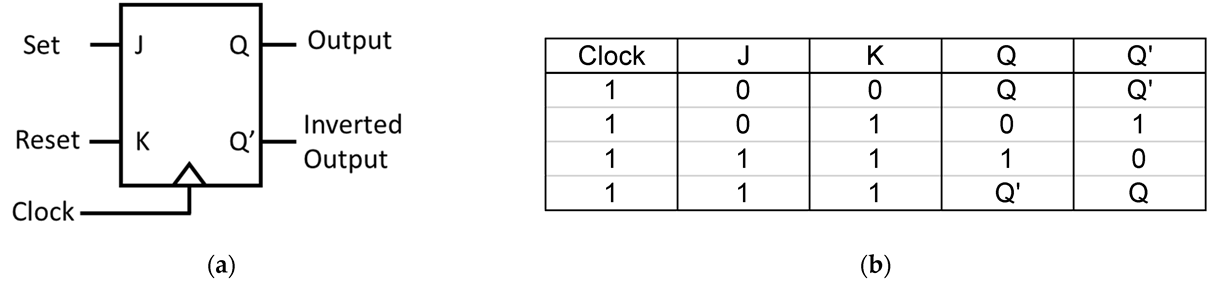
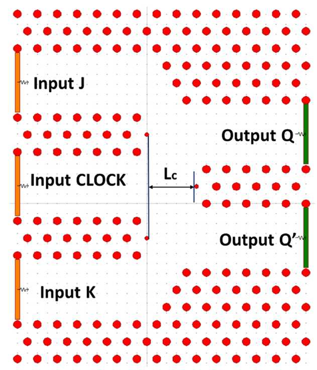
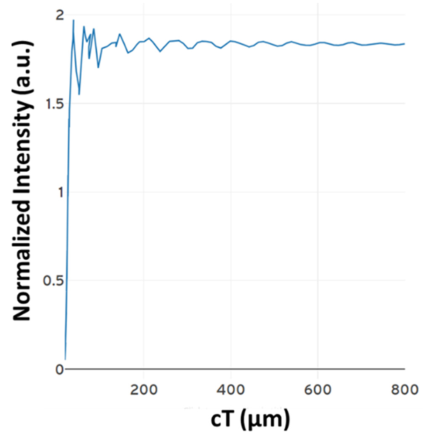
4.4. The JK Flip-Flop
5. Conclusions
Author Contributions
Funding
Conflicts of Interest
References
- Kanellos, G.T.; Alexoudi, T.; Fitsios, D.; Vagionas, C.; Maniotis, P.; Papaioannou, S.; Miliou, A.; Pleroset, N. WDM-enabled optical RAM architectures for ultra-fast, low-power optical cache memories. In Proceedings of the 15th International Conference on Transparent Optical Networks (ICTON), Cartagena, Columbia, 23–27 June 2013; pp. 1–4. [Google Scholar]
- Nataraj, M.; Levisse, A.; Giraud, B.; Noel, J.-P.; Meinerzhagen, P.; Portal, J.M.; Gaillardon, P.-E. Design methodology for area and energy efficient OxRAM-based non-volatile flip-flop. In Proceedings of the IEEE International Symposium on Circuits and Systems (ISCAS), Baltimore, MD, USA, 28–31 May 2017; pp. 1–4. [Google Scholar]
- Strollo, A.G.M.; De Caro, D.; Petra, N. A 630 MHz, 76 mW Direct Digital Frequency Synthesizer Using Enhanced ROM Compression Technique. IEEE J. Solid-State Circuits 2007, 42, 350–360. [Google Scholar] [CrossRef]
- Zheng, J.; Zeng, Z.; Zhu, Y. Memristor-based nonvolatile synchronous flip-flop circuits. In Proceedings of the Seventh International Conference on Information Science and Technology (ICIST), Da Nang, Vietnam, 16–19 April 2017; pp. 504–508. [Google Scholar]
- Verma, V.J.; Mishra, A.K.; Vaithiyanathan, D.; Kaur, B. Review of Different Flip-Flop Circuits and a Modified Flip-Flop Circuit for Low Voltage Operation. In Proceedings of the IEEE 3rd Global Conference for Advancement in Technology (GCAT), Bangalore, India, 7–9 October 2022; pp. 1–5. [Google Scholar]
- Prakash, G.; Sathishkumar, K.; Sakthibharathi, B.; Saravanan, S.; Vijaysai, R. Achieveing reduced area by Multi-bit Flip flop design. In Proceedings of the International Conference on Computer Communication and Informatics, Coimbatore, India, 4–6 January 2013; pp. 1–4. [Google Scholar]
- Chiang, M.F.; Ghassemlooy, Z.; Ng, W.P.; Minh, H.L.; Lu, C. Ultra-fast all-optical packet-switched routing with a hybrid header address correlation Scheme. In Proceedings of the International Conference on High Performance Switching and Routing, Shanghai, China, 15–17 May 2008; pp. 92–97. [Google Scholar]
- Yoo, S.J.B.; Lee, H.J.; Vaidianathan, S.; Okamoto, K.; Kamei, S. Optical-label switching and routing by rapidly tunable wavelength conversion and uniform loss cyclic frequency array-waveguide grating. In Proceedings of the Optical Fiber Communication Conference and Exhibit, Anaheim, CA, USA, 17–22 March 2001; p. WDD49. [Google Scholar]
- Areed, N.F.F.; Obayya, S.S.A. Novel All-Optical Liquid Photonic Crystal Router. IEEE Photonics Technol. Lett. 2013, 25, 1254–1257. [Google Scholar] [CrossRef]
- Mendinueta, J.M.D.; Shinada, S.; Hirota, Y.; Luís, R.S.; Furukawa, H.; Wada, N. Optical Switching System for Next Generation Data Center Networks with Time-division Spatial Super-channels and Core-joint Optical Switches. In Proceedings of the Photonics in Switching and Computing (PSC), Limassol, Cyprus, 19–21 September 2018; pp. 1–3. [Google Scholar]
- Iino, K.; Kita, T. Ultra-Fast Optical Switching Using Differential Control Method. In Proceedings of the European Conference on Optical Communication (ECOC), Basel, Switzerland, 18–22 September 2022; pp. 1–4. [Google Scholar]
- Solus, D.; Ovsenik, E.; Turan, J. Usage of optical correlator in video surveillance system for abandoned luggage. In Proceedings of the IEEE 14th International Scientific Conference on Informatics, Poprad, Slovakia, 14–16 November 2017; pp. 349–352. [Google Scholar]
- Ovseník, C.; Turán, J.; Kolesárová, A.K. Video surveillance systems with optical correlator. In Proceedings of the 34th International Convention MIPRO, Opatija, Croatia, 23–27 May 2011; pp. 227–230. [Google Scholar]
- Barbut, C. Fiber Optic Deployments in Romania between Metropolitan Fiber Optic Networks and Indoor Fiber Optic Infrastructure. In Proceedings of the 10th International Conference on Electronics, Computers and Artificial Intelligence (ECAI), Iasi, Romania, 28–30 June 2018; pp. 1–3. [Google Scholar]
- Jing, J.; Liu, K.; Jiang, J.; Xu, T.; Wang, S.; Ma, J.; Zhang, Z.; Zhang, W.; Liu, T. Theoretical Investigation of Optical Fiber Waveguide Coupled Surface Plasmon Resonance Sensor with Narrow Full Width at Half-Maximum. In Proceedings of the 19th International Conference on Optical Communications and Networks (ICOCN), Qufu, China, 23–27 August 2021; pp. 1–2. [Google Scholar]
- Bromage, J.; Bouteiller, J.-C.; Thiele, H.J.; Brar, K.; Park, J.H.; Headley, C.; Nelson, L.E.; Qian, Y.; DeMarco, J.; Stulz, S.; et al. S-band all-Raman amplifiers for 40/spl times/10 Gb/s transmission over 6/spl times/100 km of non-zero dispersion fiber. In Proceedings of the Optical Fiber Communication Conference and Exhibit, Anaheim, CA, USA, 17–22 March 2001; p. PD4. [Google Scholar]
- Krishnamoorthy, A.V.; Lexau, J.; Zheng, X.; Cunningham, J.E.; Ho, R.; Torudbakken, O. Optical Interconnects for Present and Future High-Performance Computing Systems. In Proceedings of the 16th IEEE Symposium on High Performance Interconnects, Stanford, CA, USA, 26–28 August 2008; pp. 175–177. [Google Scholar]
- Onaka, H.; Kinoshita, S.; Aoki, Y. WDM Optical Packet Interconnection for Petascale Ultra-High-Performance Computing Systems. In Proceedings of the Photonics in Switching, San Francisco, CA, USA, 19–22 August 2007; pp. 57–58. [Google Scholar]
- Hadzialic, S.; Kim, S.; Sudbo, A.S.; Solgaard, O. Two-Dimensional Photonic Crystals Fabricated in Monolithic Single-Crystal Silicon. IEEE Photonics Technol. Lett. 2010, 22, 67–69. [Google Scholar] [CrossRef]
- Monsoriu, J.; Silvestre, E.; Ferrando, A.; Andres, P.; Andres, M. Sloped-wall thin-film photonic crystal waveguides. IEEE Photonics Technol. Lett. 2005, 17, 354–356. [Google Scholar] [CrossRef]
- Katz, O.; Malka, D. Design of novel SOI 1 × 4 optical power splitter using seven horizontally slotted waveguides. Photonics Nanostructures–Fundam. Appl. 2017, 25, 9–13. [Google Scholar] [CrossRef]
- Malka, D.; Peled, A. Power splitting of 1 × 16 in multicore photonic crystal fibers. Appl. Surf. Sci. 2017, 417, 34–39. [Google Scholar] [CrossRef]
- Malka, D.; Cohen, E.; Zalevsky, Z. Design of 4 × 1 Power Beam Combiner Based on MultiCore Photonic Crystal Fiber. Appl. Sci. 2017, 7, 695. [Google Scholar] [CrossRef]
- Zhang, Y.; Qiu, X.; Zeng, C.; Li, D.; Gao, G.; Wang, Y.; Yu, J.; Xia, J. Slow-Light Dispersion in One-Dimensional Photonic Crystal Racetrack Ring Resonator. IEEE Photon. Technol. Lett. 2015, 27, 1120–1123. [Google Scholar] [CrossRef]
- Zhang, Q.; Li, X. One-Way Rotating Photonic Crystal Ring Resonator with High Quality Factor. IEEE Photon. J. 2018, 10, 4700110. [Google Scholar] [CrossRef]
- Han, T.Y.; Lee, H.-S.; Lee, E.-H. Design of compact silicon optical modulator using Photonic Crystal MZI structure. In Proceedings of the 5th IEEE International Conference on Group IV Photonics, Sorrento, Italy, 17–19 September 2008; pp. 308–310. [Google Scholar]
- Qi, B.; Yu, P.; Li, Y.; Hao, Y.; Zhou, Q.; Jiang, X.; Yang, J. Ultracompact Electrooptic Silicon Modulator with Horizontal Photonic Crystal Slotted Slab. IEEE Photon.-Technol. Lett. 2010, 22, 724–726. [Google Scholar] [CrossRef]
- Saitoh, K.; Florous, N.J.; Varshney, S.K.; Koshiba, M. Tunable Photonic Crystal Fiber Couplers with a Thermo-Responsive Liquid Crystal Resonator. J. Light. Technol. 2008, 26, 663–669. [Google Scholar] [CrossRef]
- Chien, H.-T.; Chen, C.-C. Waveguide coupler formed by a graded photonic crystal. In Proceedings of the Conference on Optical Fiber Communication, San Diego, CA, USA, 22–26 March 2009; pp. 1–3. [Google Scholar]
- Hsiao, L.-T.; Yu, C.-P. Mach-Zehnder fiber interferometers based on liquid-filled photonic crystal fibers. In Proceedings of the 21st Annual Wireless and Optical Communications Conference (WOCC), Kaohsiung, Taiwan, 19–21 April 2012; pp. 146–148. [Google Scholar]
- Lim, J.L.; Hu, D.J.J.; Shum, P.P.; Wang, Y. Cascaded Photonic Crystal Fiber Interferometers for Refractive Index Sensing. IEEE Photon. J. 2012, 4, 1163–1169. [Google Scholar]
- Yu, Y.; Hu, H.; Oxenlowe, L.K.; Yvind, K.; Mork, J. Ultrafast low-energy all-optical switching using a photonic-crystal asymmetric Fano structure. In Proceedings of the International Conference on Photonics in Switching (PS), Florence, Italy, 22–25 September 2015; pp. 94–96. [Google Scholar]
- Subhalakshmi, G.; Robinson, S. Design and Analysis of Optical Logic Gate using Two Dimension Photonic Crystal. In Proceedings of the International Conference on Current Trends towards Converging Technologies (ICCTCT), Coimbatore, India, 1–3 March 2018; pp. 1–5. [Google Scholar]
- Pugachov, Y.; Gulitski, M.; Mizrahi, O.; Malka, D. Design of All-Optical Logic Half-Adder Based on Photonic Crystal Multi-Ring Resonator. Symmetry 2023, 15, 1063. [Google Scholar] [CrossRef]
- Sato, T.; Fujisawa, T.; Saitoh, K. Novel All-Optical Diode Based on Single-Port and Four-Port Photonic Crystal Cavities. In Proceedings of the 23rd Opto-Electronics and Communications Conference (OECC), Jeju, Republic of Korea, 2–6 July 2018; pp. 1–2. [Google Scholar]
- Sato, T.; Fujisawa, T.; Saitoh, K. All-Optical Diode Suppressing Broadband Backward Transmission Using Single- and Four-Port Photonic Crystal Cavities. IEEE Photonics J. 2019, 11, 4900214. [Google Scholar] [CrossRef]
- Qiao, Q.; Lee, C.; Zhou, G. Thermal Infrared Sensor Based on Coupled Photonic Crystal Nanobeam Cavities. In Proceedings of the International Conference on Optical MEMS and Nanophotonics (OMN), Lausanne, Switzerland, 29 July–2 August 2018; pp. 1–2. [Google Scholar]
- Frazao, O.; Baptista, J.M.; Santos, J.L. Temperature-Independent Strain Sensor Based on a Hi-Bi Photonic Crystal Fiber Loop Mirror. IEEE Sens. J. 2007, 7, 1453–1455. [Google Scholar] [CrossRef]
- Almawgani, A.H.M.; Alhamss, D.N.; Taya, S.A.; Hindi, A.T.; Upadhyay, A.; Singh, S.; Colak, I.; Pal, A.; Patel, S.K. Theoretical analysis of a refractive index sensor based on a photonic crystal fiber with a rectangular core. Opt. Quantum Electron. 2023, 55, 881. [Google Scholar] [CrossRef]
- Almawgani, A.H.M.; Alhamss, D.N.; Taya, S.A.; Colak, I.; Sharma, A.; Alhawari, A.R.H.; Patel, S.K. The properties of a tunable terahertz filter based on a photonic crystal with a magnetized plasma defect layer. Phys. Fluids 2022, 34, 082020. [Google Scholar] [CrossRef]
- Mehdizadeh, F.; Soroosh, M.; Alipour-Banaei, H.; Farshidi, E. A Novel Proposal for All Optical Analog-to-Digital Converter Based on Photonic Crystal Structures. IEEE Photon.- J. 2017, 9, 4700311. [Google Scholar] [CrossRef]
- Sharkway, A.; Chen, C.; Miao, B.; Shi, S.; Prather, D. Development of an Analog-to-Digital Converter Using Photonic Crystals. In Proceedings of the Conference on Lasers and Electro-Optics (CLEO), Baltimore, MD, USA, 6–11 May 2007; pp. 1–2. [Google Scholar]
- Gelkop, B.; Aichnboim, L.; Malka, D. RGB wavelength multiplexer based on polycarbonate multicore polymer optical fiber. Opt. Fiber Technol. 2021, 61, 102441. [Google Scholar] [CrossRef]
- Malka, D.; Zalevsky, Z.; Sintov, Y. Design of a 1 × 4 silicon wavelength demultiplexer based on multimode interference in a slot waveguide structures. In Proceedings of the IEEE 28th Convention of Electrical & Electronics Engineers in Israel (IEEEI), Eilat, Israel, 3–5 December 2014; pp. 1–4. [Google Scholar]
- Buzaverov, K.A.; Baburin, A.S.; Sergeev, E.V.; Avdeev, S.S.; Lotkov, E.S.; Andronik, M.; Stukalova, V.E.; Baklykov, D.A.; Dyakonov, I.V.; Skryabin, N.N.; et al. Low-loss silicon nitride photonic ICs for near-infrared wavelength bandwidth. Opt. Express 2023, 31, 16227–16242. [Google Scholar] [CrossRef]
- Luke, K.; Kharel, P.; Reimer, C.; He, L.; Loncar, M.; Zhang, M. Wafer-scale low-loss lithium niobate photonic integrated circuits. Opt. Express 2020, 28, 24452–24458. [Google Scholar] [CrossRef]
- Van der Tol, J.; Pello, J.; Bhat, S.; Jiao, Y.; Heiss, D.; Roelkens, G.; Ambrosius, H.; Smit, M. Photonic integration in indium-phosphide membranes on silicon (IMOS). In Proceedings of the Society for Optical Instrumentation Engineering, San Francisco, CA, USA, 8 March 2014; Volume 8988. [Google Scholar]
- Humbert, G.; Wang, Y.; Light, P.S.; Benabid, F.; Roberts, P.J. Roberts Nonlinear effects in a silica-node of a hollow-core photonic crystal fiber within the photonic bandgap. In Proceedings of the Conference on Lasers and Electro-Optics and 2008 Conference on Quantum Electronics and Laser Science, San Jose, CA, USA, 4–9 May 2008; pp. 1–2. [Google Scholar]
- Hache, A.; Bourgeois, M. Optical modulation of a photonic bandgap with two-photon excitation and the Kerr effect. In Proceedings of the Technical Digest. Summaries of papers presented at the Quantum Electronics and Laser Science Conference, Baltimore, MD, USA, 11 May 2001; pp. 157–158. [Google Scholar]
- Gong, C.; Ho, X. Two-dimensional Photonic Crystals with a Large Photonic Band Gap Designed by a Rapid Genetic Algorithm. In Proceedings of the 1st IEEE International Conference on Nano/Micro Engineered and Molecular Systems, Zhuhai, China, 18–21 January 2006; pp. 475–478. [Google Scholar]
- Zhang, J.; Yuan, J.; Qu, Y.; Qiu, S.; Zhou, X.; Yan, B.; Wu, Q.; Wang, K.; Sang, X.; Yu, C. A novel photonic crystal fiber refractive index sensor based on surface plasmon resonance effect with wide detection range. In Proceedings of the 19th International Conference on Optical Communications and Networks (ICOCN), Qufu, China, 23–27 August 2021; pp. 1–3. [Google Scholar]
- Malik, M.A.; Sharma, V.K. Design of low power SR-flip-flop with on/off (ONOFIC) implementation. In Proceedings of the International Conference on Communication and Electronics Systems (ICCES), Coimbatore, India, 17–19 July 2019; pp. 101–103. [Google Scholar]
- Ashwini, H.; Rohith, S.; Sunitha, K.A. Implementation of high speed and low power 5T-TSPC D flip-flop and its application. In Proceedings of the International Conference on Communication and Signal Processing (ICCSP), Melmaruvathur, India, 6–8 April 2016; pp. 0275–0279. [Google Scholar]
- Zhao, X.; Guo, J.; Song, G. An improved low-power clock-gating pulse-triggered JK flip-flop. In Proceedings of the 2010 International Conference on Information, Networking and Automation (ICINA), Kunming, China, 18–19 October 2010; pp. V2-489–V2-491. [Google Scholar]
- Shimizu, S.; Uenohara, H. A proposal and analytical investigation of all-optical T-type Flip-Flop using SOAs. In Proceedings of the International Conference on Photonics in Switching, Pisa, Italy, 15–19 September 2009; pp. 1–2. [Google Scholar]
- Shoresh, T.; Katanov, N.; Malka, D. 1 × 4 MMI visible light wavelength demultiplexer based on a GaN slot-waveguide structure. Photonics Nanostructures Fundam. Appl. 2018, 30, 45–49. [Google Scholar] [CrossRef]
- Cheng, T.H. All-optical photonic packet switching revisited: What has changed and what has not changed after 20 years? In Proceedings of the 9th International Conference on Optical Communications and Networks, Nanjing, China, 24–27 October 2010; pp. 235–240. [Google Scholar]
- Wang, Y. Nonlinear optical limiter and digital optical switch by cascaded nonlinear couplers: Analysis. J. Light. Technol. 1999, 17, 292–297. [Google Scholar] [CrossRef]
- Giancarlo, P.; Luca, P.; Bogoni, A. The all-optical flip-flop: State-of-the-art and perspectives. In Proceedings of the International Society for Optical Instrumentation Engineering, Hangzhou, China, 11 November 2008; Volume 7136. [Google Scholar]
- Notomi, M.; Tanabe, T.; Shinya, A.; Kuramochi, E.; Taniyama, H.; Mitsugi, S.; Morita, M. Nonlinear and adiabatic control of high-Q photonic crystal nanocavities. Opt. Express 2007, 15, 17458–17481. [Google Scholar] [CrossRef]
- Maes, B.; Bienstman, P.; Baets, R. A novel photonic crystal flip-flop device. In Proceedings of the Nonlinear Guided Waves and Their Applications, Toronto, Canada, 28–31 March 2004. [Google Scholar]
- Shinya, A.; Mitsugi, S.; Tanabe, T.; Notomi, M.; Yokohama, I.; Takara, H.; Kawanishi, S. All-optical flip-flop circuit composed of coupled two-port resonant tunneling filter in two-dimensional photonic crystal slab. Opt. Express 2006, 14, 1230–1235. [Google Scholar] [CrossRef] [PubMed]
- Damodaran, S.; Shankar, T.; Anbazhagan, R. All optical clocked D flip flop for 1.72 Tb/s optical computing. Microelectron. J. 2020, 103, 26–2692. [Google Scholar] [CrossRef]
- Shaik, E.H.; Rangaswamy, N. Investigation on photonic crystal based all-optical clocked D-flip flop. IET Optoelectron. 2017, 11, 148–155. [Google Scholar] [CrossRef]
- Rao, D.G.S.; Palacharla, V.; Swarnakar, S.; Kumar, S. Design of all-optical D flip-flop using photonic crystal waveguides for optical computing and networking. Appl. Opt. 2020, 59, 7139–7143. [Google Scholar] [CrossRef] [PubMed]
- Taylor, J.; Tanev, S. Photonic Simulation Software Tools for Education. In Proceedings of the Education and Training in Optics and Photonics, OSA Technical Digest Series, Ottawa, Canada, 3 June 2007. [Google Scholar]
- Hassan, A.; Areed, N.F.F.; Obayya, S.A.; He, M. Efficient and Compact SR-flip Flop Optical Memory Based Photonic Crystals Platform. Res. Sq. 2021. [Google Scholar] [CrossRef]
- Zamanian-Dehkordi, S.S.; Soroosh, M.; Akbarizadeh, G. An ultra-fast all-optical RS flip-flop based on nonlinear photonic crystal structures. Opt. Rev. 2018, 25, 523–531. [Google Scholar] [CrossRef]
- Soma, S.; Sonth, M.V.; Gowre, S.C. Design of two-dimensional photonic crystal based ultra compact optical RS flip-flop. Photon. Netw. Commun. 2022, 43, 109–115. [Google Scholar] [CrossRef]
- Valliammai, M.; Mohanraj, J.; Kanimozhi, T.; Sridevi, S. Design of all-optical Chalcogenide T-flip flop using Photonic Crystal Waveguide. In Proceedings of the International Conference on Numerical Simulation of Optoelectronic Devices (NUSOD), Turin, Italy, 13–17 September 2021; pp. 133–134. [Google Scholar]
- Rao, K.M.K.; Aneela, N.J.; Sri, K.Y.; Prasanna, K.N.; Sahithi, N.; Likhitha, L. Design of Clocked Jk Flip Flop Using Air Hole Structured Photonic Crystal. J. VLSI Circuits Syst. 2021, 3, 11–20. [Google Scholar]
- Stojanovic, V.; Oklobdzija, V. Comparative analysis of master-slave latches and flip-flops for high-performance and low-power systems. IEEE J. Solid-State Circuits 1999, 34, 536–548. [Google Scholar] [CrossRef]
- Clavero, R.; Ramos, F.; Martinez, J.; Marti, J. All-optical flip-flop based on a single SOA-MZI. EEE Photon. Technol. Lett. 2005, 17, 843–845. [Google Scholar] [CrossRef]
- Dorren, H.J.S.; Lenstra, D.; Liu, Y.; Hill, M.T.; Khoe, G.-D. Nonlinear polarization rotation in semiconductor optical amplifiers: Theory and application to all-optical flip-flop memories. IEEE J. Quantum Electron. 2003, 39, 141–148. [Google Scholar] [CrossRef]

| Mode | Propagation Constant at Wavelength of 1650 nm | Coupling Length (Lc) (μm) |
|---|---|---|
| Fundamental | 0.36 | 21.2a |
| First Order | 0.32 | 18.6a |
| Second Order | 0.28 | 8.2a |
| Third Order | 0.17 | 2.5a |
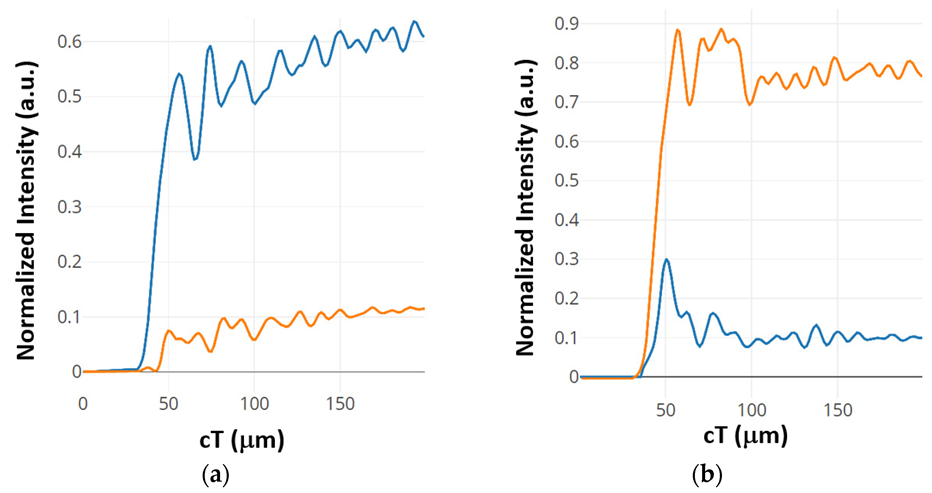
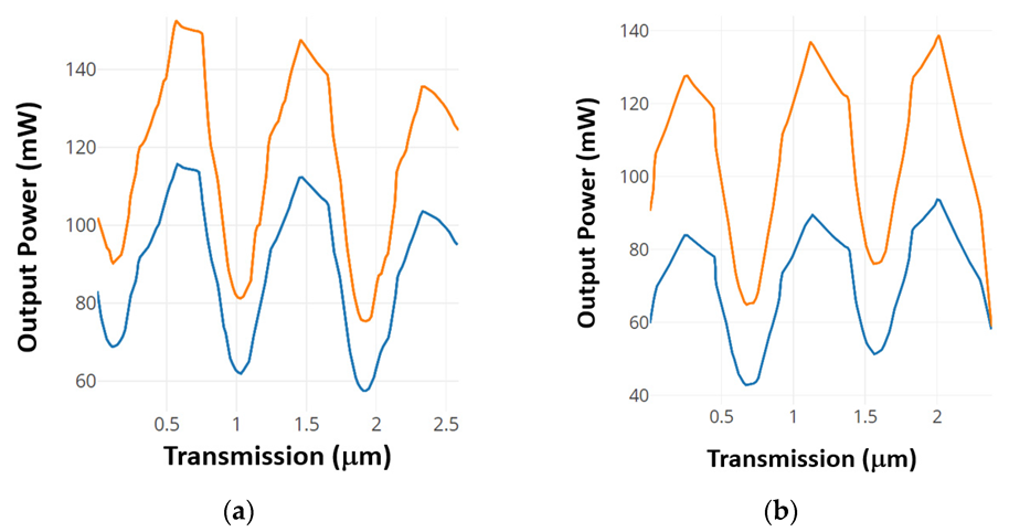
| Q | Pout | CR | Q’ | Pout | CR |
|---|---|---|---|---|---|
| 0 | 0.216 | 8.657 | 21.2a | 0.204 | 8.568 |
| 1 | 1.571 | 18.6a | 1.498 |
| Type of Structure | Mechanisms and Effects | Response Time (psec) | Contrast Ratio (dB) | Footprint (μm2) | Operating Wavelength (nm) | Year |
|---|---|---|---|---|---|---|
| Linear square lattice of Si * and chalcogenide glass ** rods in air [63] | Ring resonator, coupling rods and scattering rods | 0.063 | 11.13 * 9.711 ** | 71.14 | 1550 | 2020 |
| Linear square lattice of Si rods in air [64] | MMI, edge rods point defects | 0.29 | 9.63 | 71.28 | 1550 | 2017 |
| Linear square lattice of Si rods in air [65] | T-shaped waveguides | - | 13.5 | 45.36 | 1550 | 2020 |
| Linear square lattice of Si rods in air [67] | T-type switches, ring resonators and Y-splitters | 1.2 | 6.99 | 836 | 1600 (SET) 1580 (RESET) | 2021 |
| Non-linear square lattice dielectric rods in air [68] | cross-connected resonant cavities and optical switches | 3.1 | 9.68 | 361 | 1586 1620 | 2018 |
| Linear hexagonal lattice Si rods in air [69] | Ring resonators and Y-splitters | 1.2 | 8.7 | 784 | 1550 | 2022 |
| Linear square lattice chalcogenide rods in air [70] | XOR gate, D FF, chalcogenide rods | 0.16 | 16.68 | 38.85 | 1550 | 2021 |
| Air holes in GaAs PC configuration [71] | MMI, scattering rods | 0.27 | 8.657 | 78.75 | 1650 | 2021 |
Disclaimer/Publisher’s Note: The statements, opinions and data contained in all publications are solely those of the individual author(s) and contributor(s) and not of MDPI and/or the editor(s). MDPI and/or the editor(s) disclaim responsibility for any injury to people or property resulting from any ideas, methods, instructions or products referred to in the content. |
© 2023 by the authors. Licensee MDPI, Basel, Switzerland. This article is an open access article distributed under the terms and conditions of the Creative Commons Attribution (CC BY) license (https://creativecommons.org/licenses/by/4.0/).
Share and Cite
Pugachov, Y.; Gulitski, M.; Malka, D. Photonic Crystal Flip-Flops: Recent Developments in All Optical Memory Components. Materials 2023, 16, 6467. https://doi.org/10.3390/ma16196467
Pugachov Y, Gulitski M, Malka D. Photonic Crystal Flip-Flops: Recent Developments in All Optical Memory Components. Materials. 2023; 16(19):6467. https://doi.org/10.3390/ma16196467
Chicago/Turabian StylePugachov, Yonatan, Moria Gulitski, and Dror Malka. 2023. "Photonic Crystal Flip-Flops: Recent Developments in All Optical Memory Components" Materials 16, no. 19: 6467. https://doi.org/10.3390/ma16196467
APA StylePugachov, Y., Gulitski, M., & Malka, D. (2023). Photonic Crystal Flip-Flops: Recent Developments in All Optical Memory Components. Materials, 16(19), 6467. https://doi.org/10.3390/ma16196467