Article

A Simple Method for the Fabrication of Silicon Inverted Pyramid Substrates for Surface-Enhanced Raman Spectroscopy

College of Materials Science and Engineering, Nanjing Tech University, 30 South PuZhu Road, Nanjing 210009, China
*
Author to whom correspondence should be addressed.
Materials 2023, 16(10), 3634; https://doi.org/10.3390/ma16103634
Submission received: 20 April 2023 / Revised: 6 May 2023 / Accepted: 8 May 2023 / Published: 10 May 2023

Abstract

:
Silicon inverted pyramids have been shown to exhibit superior SERS properties compared to ortho-pyramids, yet low-cost, simple preparation processes are lacking at present. This study demonstrates a simple method, silver-assisted chemical etching combined with PVP, to construct silicon inverted pyramids with a uniform size distribution. Two types of Si substrates for surface-enhanced Raman spectroscopy (SERS) were prepared via silver nanoparticles deposited on the silicon inverted pyramids by electroless deposition and radiofrequency sputtering, respectively. The experiments were conducted using rhodamine 6G (R6G), methylene blue (MB) and amoxicillin (AMX) molecules to test the SERS properties of the Si substrates with inverted pyramids. The results indicate that the SERS substrates show high sensitivity to detect the above molecules. In particular, the sensitivity and reproducibility of the SERS substrates with a denser silver nanoparticle distribution, prepared by radiofrequency sputtering, are significantly higher than those of the electroless deposited substrates to detect R6G molecules. This study sheds light on a potential low-cost and stable method for preparing silicon inverted pyramids, which is expected to replace the costly commercial Klarite SERS substrates.

1. Introduction

Surface-enhanced Raman scattering spectroscopy (SERS) is a spectroscopic analysis technique with great technical advantages, such as ultra-high sensitivity, fingerprinting features, a fast response, and a non-destructive nature [1,2,3,4]. It has been widely applied in various fields across different industries, e.g., food safety, bioanalysis, and drug testing [5,6,7]. Researchers believe that the SERS enhancement mechanism can be divided into electromagnetic enhancement (EM) and chemical enhancement (CM), and claim that EM enhancement plays a dominant role. EM enhancement is caused by localized surface plasmon resonance (LSPR) generated between metal nanostructures or nanoparticles [8,9]. For applications of SERS, highly reproducible, large-scale production and low-cost substrates remain a challenge [10,11]. The study of SERS substrates has been expanded from the initial precious metal materials to semiconductor materials, such as Si, due to its excellent optoelectronic properties and stability. However, the enhanced Raman effect of pure silicon is not as sensitive as that of precious metals; therefore, the synergistic effect of precious metals is needed [12,13,14]. It has previously been demonstrated that 3D structured silicon with a large specific surface area and controlled 3D structure can effectively increase the number of hot spots and further improve the sensitivity of SERS signals [15,16].
A large number of researchers have so far prepared SERS substrates in different 3D structures of silicon, such as nanowires [17,18], nanopores [19], nanocones [20], pyramids [21,22,23], and inverted pyramids [24,25]. Silicon inverted pyramids with anti-reflective properties favor multiple interactions of incident light compared to flat silicon and increase light absorption and the number of adsorption hot spots. Nevertheless, a limited number of studies on inverted pyramidal SERS substrates have been conducted, and only a few scholars have purchased commercial clathrate substrates to explore the SERS properties of inverted pyramids [26]. Furthermore, the conventional method of etching silicon inverted pyramids is often tedious, the preparation cost of plasma etching is considerably high, and the commercially available Klarite SRES substrates with inverted pyramid structures are quite expensive [11,27]. Thus, taking all these factors into consideration, it is of great interest to explore a low-cost and simple method to texturize silicon inverted pyramid SERS substrates to substitute expensive commercial inverted pyramid SERS substrates (Klarite).
Our previous study proposed a novel metal-assisted chemical etching system based on silver-assisted chemical etching combined with polyvinylpyrrolidone synergy (Ag@PVP-ACE) to produce inverted pyramidal silicon with anti-reflective properties. We demonstrated that this method greatly simplified the process and reduced the cost compared to the conventional etching of inverted pyramidal silicon [27,28,29,30]. In this paper, we finalized the experimental parameters that can be used to prepare silicon inverted pyramids with excellent anti-reflectivity and size uniformity. The SERS substrates were prepared by depositing silver nanoparticles (Ag NPs) onto the surface of the inverted pyramidal silicon using the electroless deposition method [20,31] and a radiofrequency sputtering system [1]. The SERS sensitivity at different silver deposition states was investigated with R6G [32]. In addition, MB and AMX molecules were used to verify the universal applicability of the SERS substrate [1,33]. The outcomes of this study may provide a useful guide for the construction of inverted pyramidal structured silicon SERS substrates with high reproducibility, high sensitivity, and a low cost.

2. Experimental Section

2.1. Materials

The experiments conducted in this study were based on diamond wire saw (DWS) (100) oriented p-type silicon wafers (156.75 × 156.75 mm2, thickness 180 ± 10 μm, resistivity 0.5–1.5 Ω·cm). We obtained silver nitrate (AgNO3, AR) from Sinopharm Chemical and purchased ammonia (NH3·H2O, 25%, AR) and hydrogen peroxide (H2O2, 30%, GR) from Shanghai Lingfeng Chemical Reagent Co., Shanghai, China. High-purity deionized water with resistivity of 18.25 MΩ·cm−1 was used during the experiments, and the necessary dose of ammonium hydrogen fluoride (NH4HF2, AR) was purchased from Nanjing Chemical Reagent Co., Nanjing, China. Polyvinylpyrrolidone (PVP-K88-96, AR), rhodamine 6G (R6G, AR), and methylene blue (MB, AR) were provided by Shanghai Aladdin Biochemical Technology Co., Shanghai, China. All chemicals were purchased and used directly.

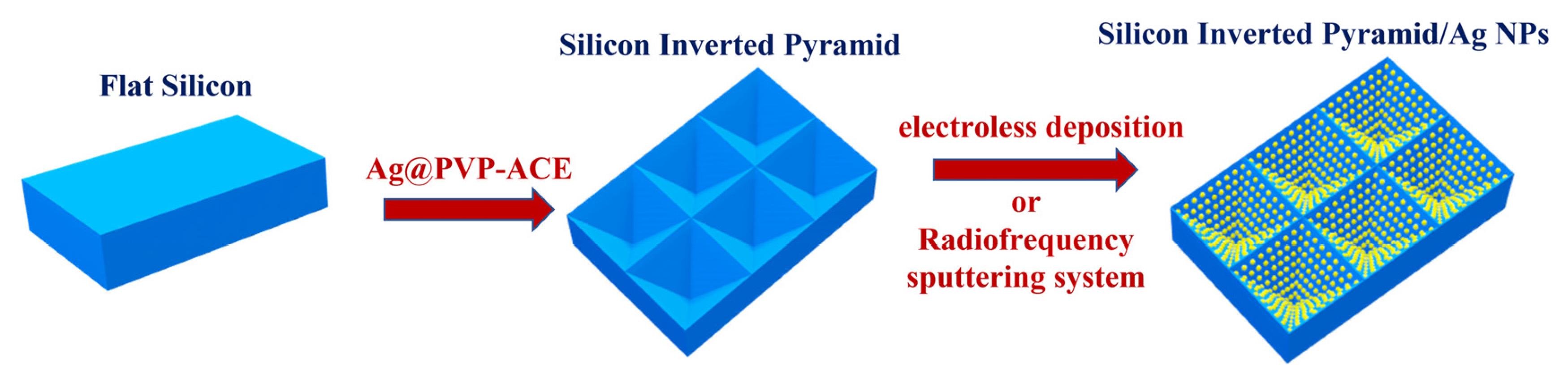
2.2. Fabrication of Silicon Inverted Pyramid/Ag NPs

Figure 1 illustrates the fabrication process of the silicon inverted pyramid/Ag NP SERS substrate. Silver-assisted chemical etching was used for the experiments, and the optimal reaction temperature was set at 65 °C, following the standards of our previous research [28]. Before etching, all silicon wafers had to be primarily polished to form flat silicon. Texturing of the flat silicon wafers with an etching solution of NH4HF2, H2O2, PVP, and AgNO3 was performed at 65 °C for a certain time. Then, the Ag NPs remaining on the silicon surface were removed with a solution of 5% NH3·H2O/5% H2O2, followed by a deionized rinse of the wafer for 1 min. Different experimental parameters were adjusted to explore their effects on the etched inverted pyramid morphology. The silicon inverted pyramid substrate with anti-reflective properties facilitates multiple interactions of the incident light, while the uniform structure of the substrate facilitates the homogeneity of the Raman data.
The silicon inverted pyramids were decorated with silver nanoparticles using the following methods: (1) electroless deposition by immersing the textured Si wafers in AgNO3 (0.5 mM) and HF (9% v/v) aqueous solution for different time periods, and then washing the wafers with deionized water, followed by air drying at room temperature; (2) in a radiofrequency sputtering system, the MS600B high-throughput multi-target magnetron sputter coater with a sputtering power of 15 w was selected to deposit silver nanoparticles on the textured Si wafers.

2.3. Characterization

The surface micromorphology of the Si wafers was observed by scanning electron microscopy (SEM, JSM-IT200, Tokyo, Japan) and field emission scanning electron microscopy (FESEM, Hitachi, 4800, Tokyo, Japan) at an accelerating voltage of 5 kV. After this, it was possible to measure the reflectance spectra of the samples in the wavelength range of 350–1050 nm with a UV–Vis–NIR spectrophotometer (UV-3101PC, Tokyo, Japan).

2.4. SERS Measurements

Rhodamine 6G (R6G) molecules were used as chemical targets to evaluate the SERS responses of the silicon inverted pyramid/Ag NPs substrates. In addition, we used methylene blue (MB) and amoxicillin (AMX) molecules to demonstrate the universal applicability of this substrate. R6G, MB, and AMX molecules were diluted in deionized water. The silicon inverted pyramid/Ag NP substrates were immersed in different concentrations of target solutions at room temperature for 30 min in the dark, and then dried naturally at room temperature. The Raman microscope system (HORIBA XploRA PLUS, Shanghai, China) was equipped with a 532 nm laser to acquire SERS spectra. For Raman measurements, the test conditions were consistent for all samples, with an acquisition time of 30 s, an acquisition exposure time of 1 s, an irradiation power of 1 mW for the laser, and a 50× objective with a 0.5 NA (numerical aperture) value. SERS spectra were collected from different regions of the samples to ensure data accuracy. Furthermore, bare silicon with a flat surface and no metal nanoparticles was used as a reference sample for normal Raman spectroscopy with the R6G concentration of 0.1 M.

3. Results and Discussion

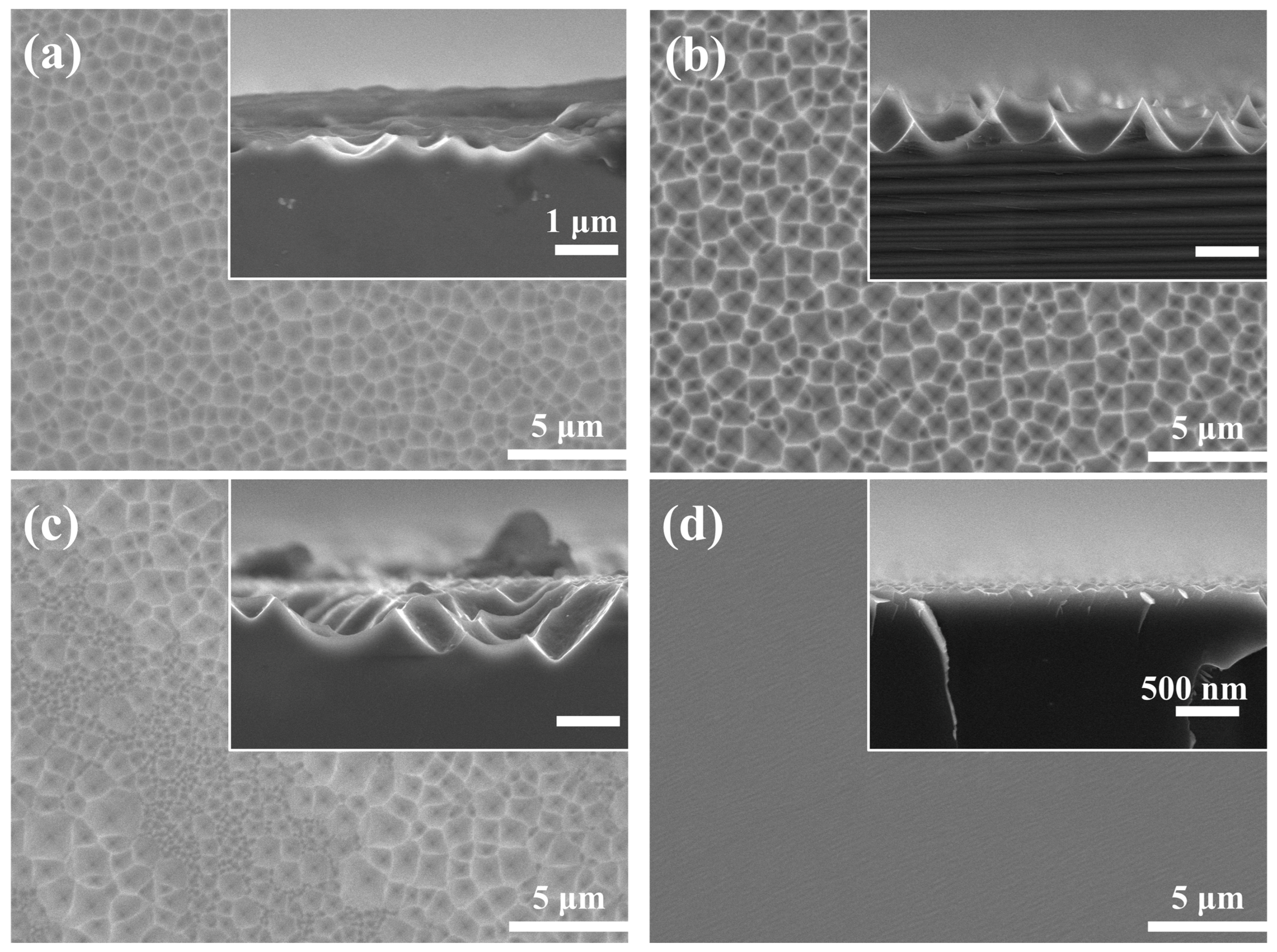
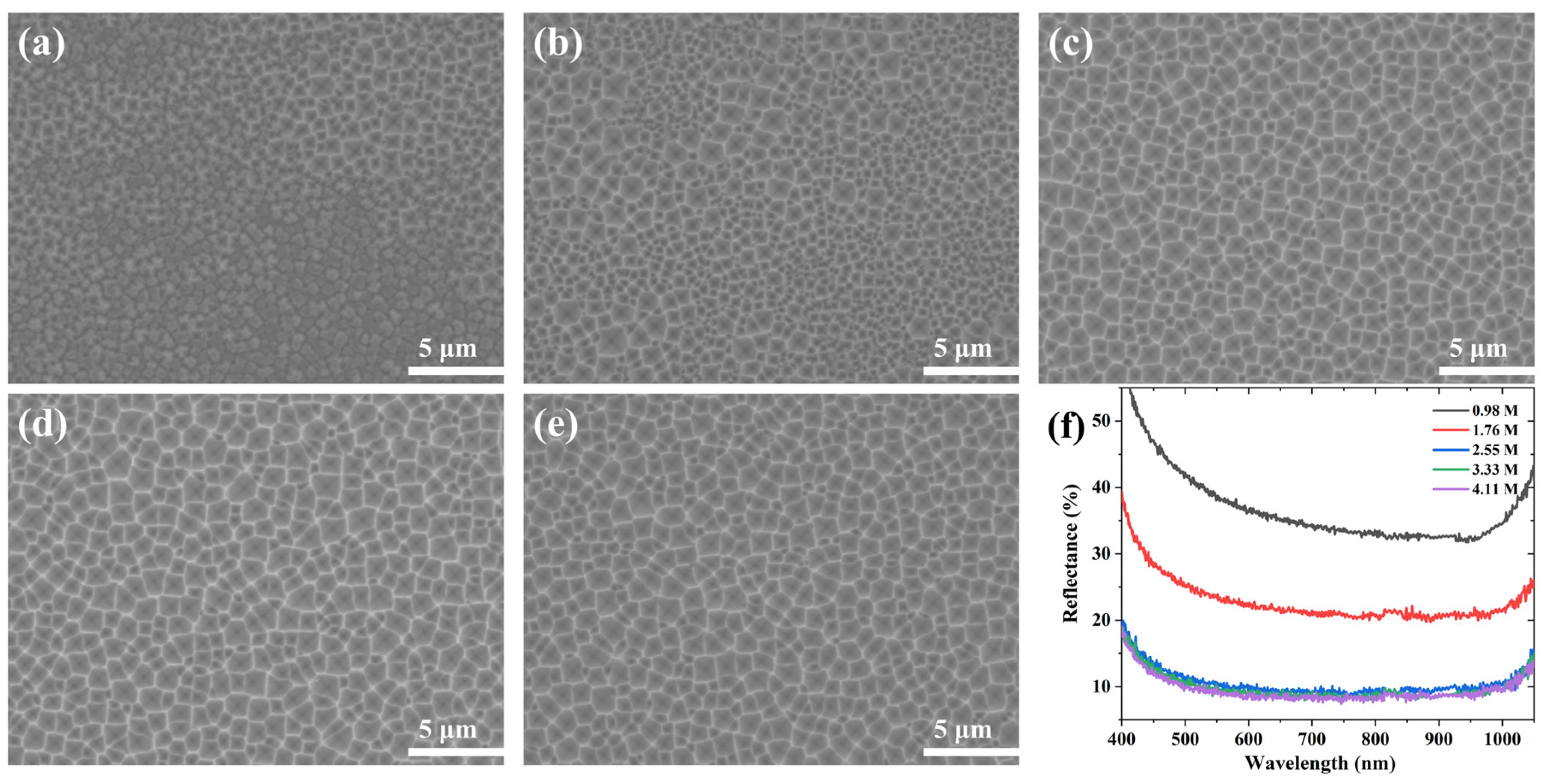
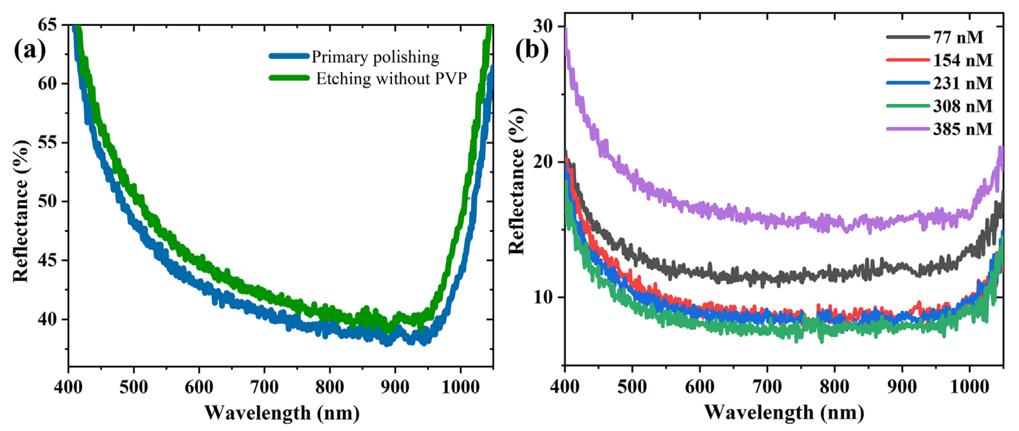
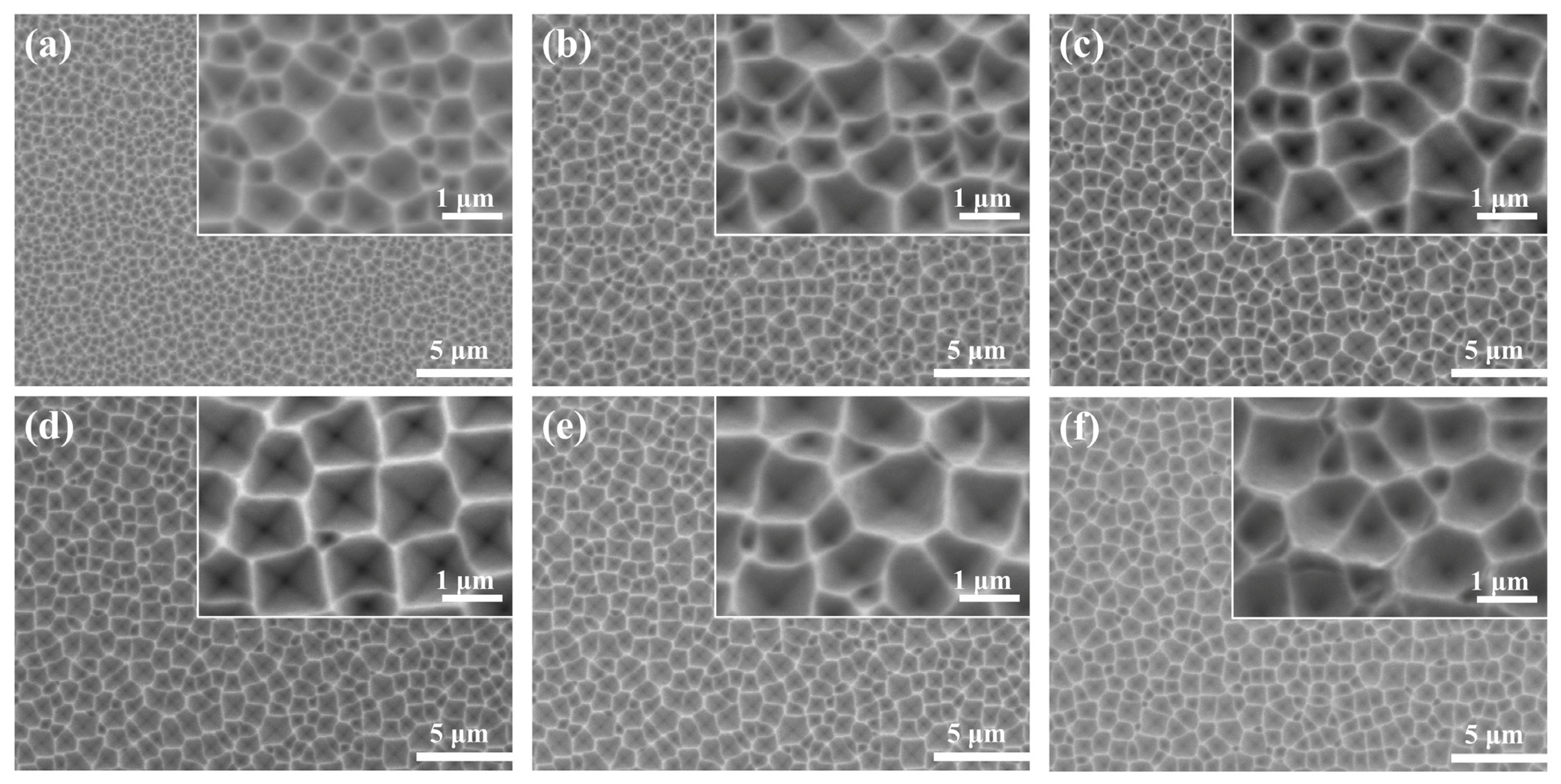
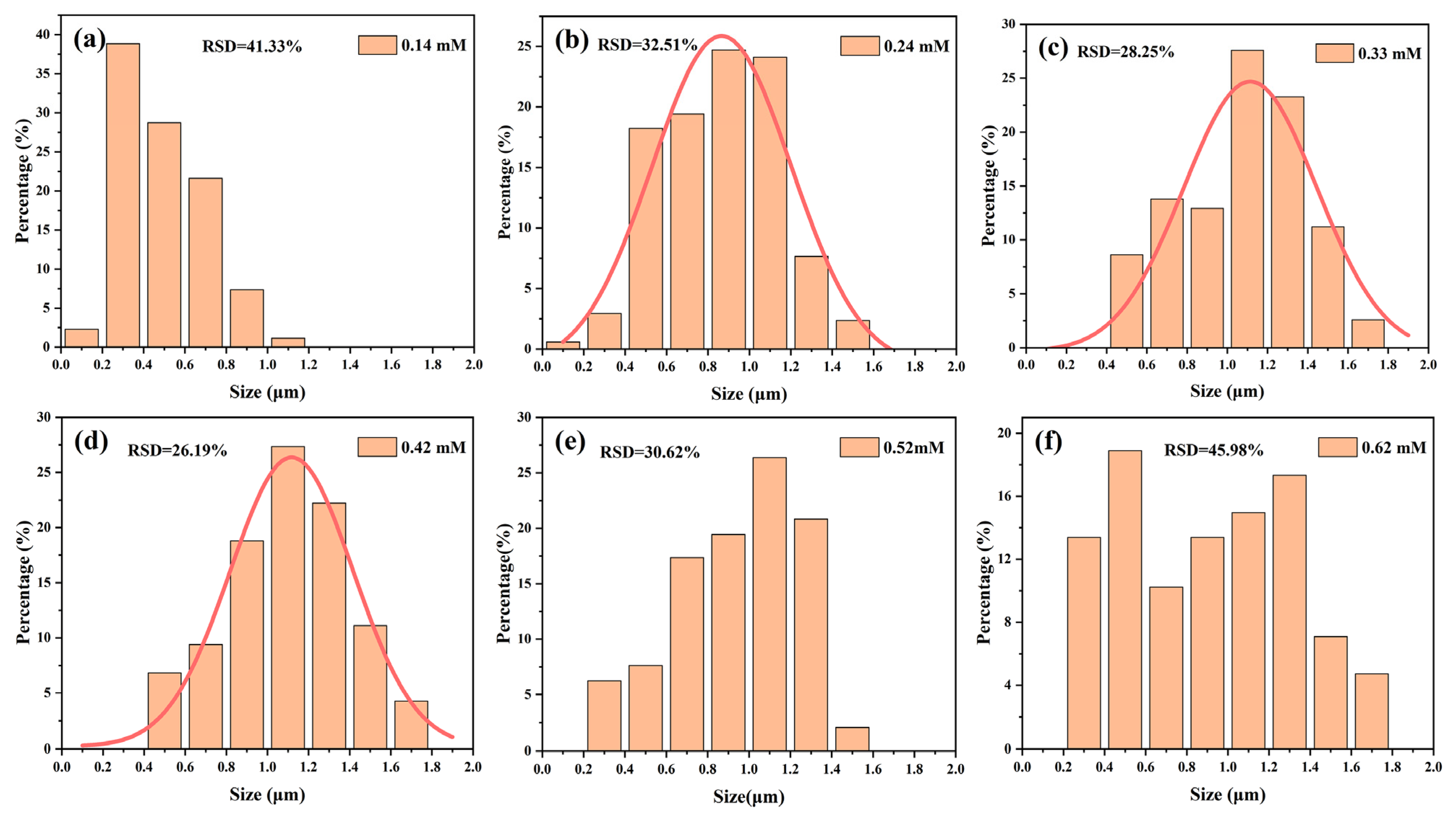
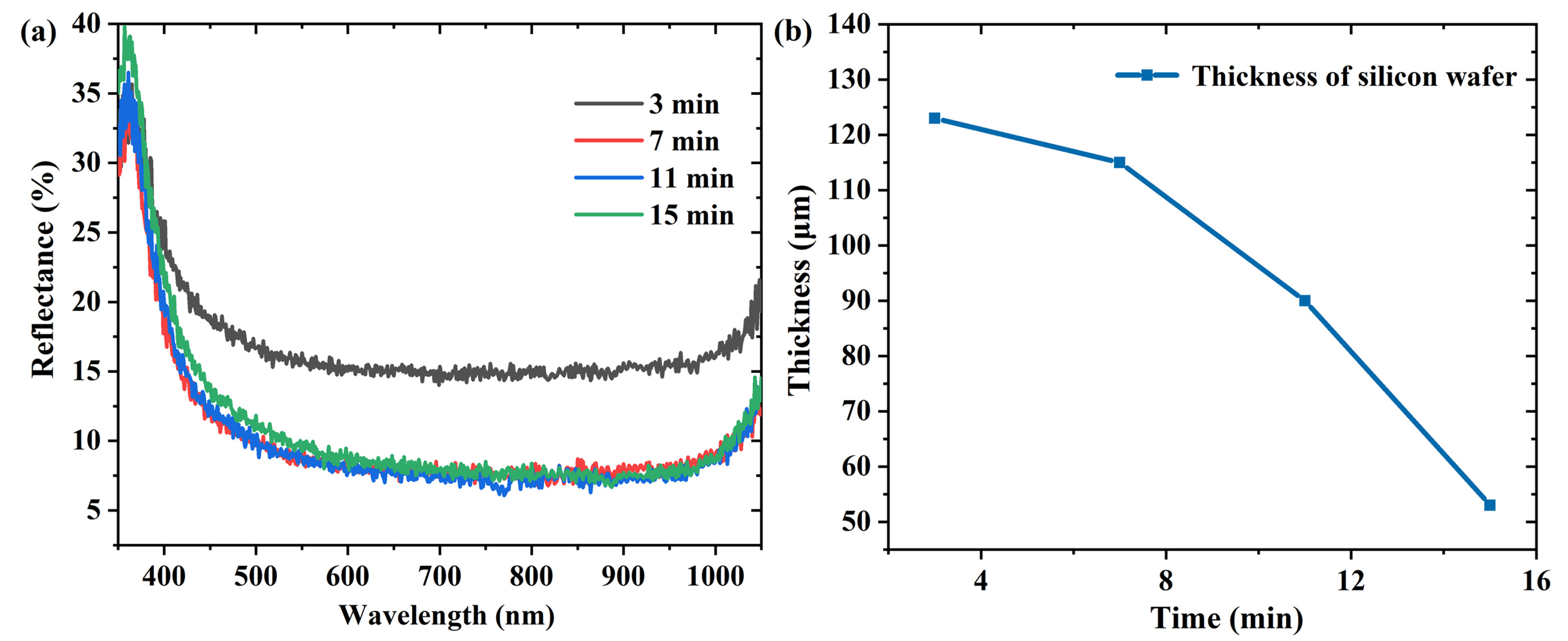
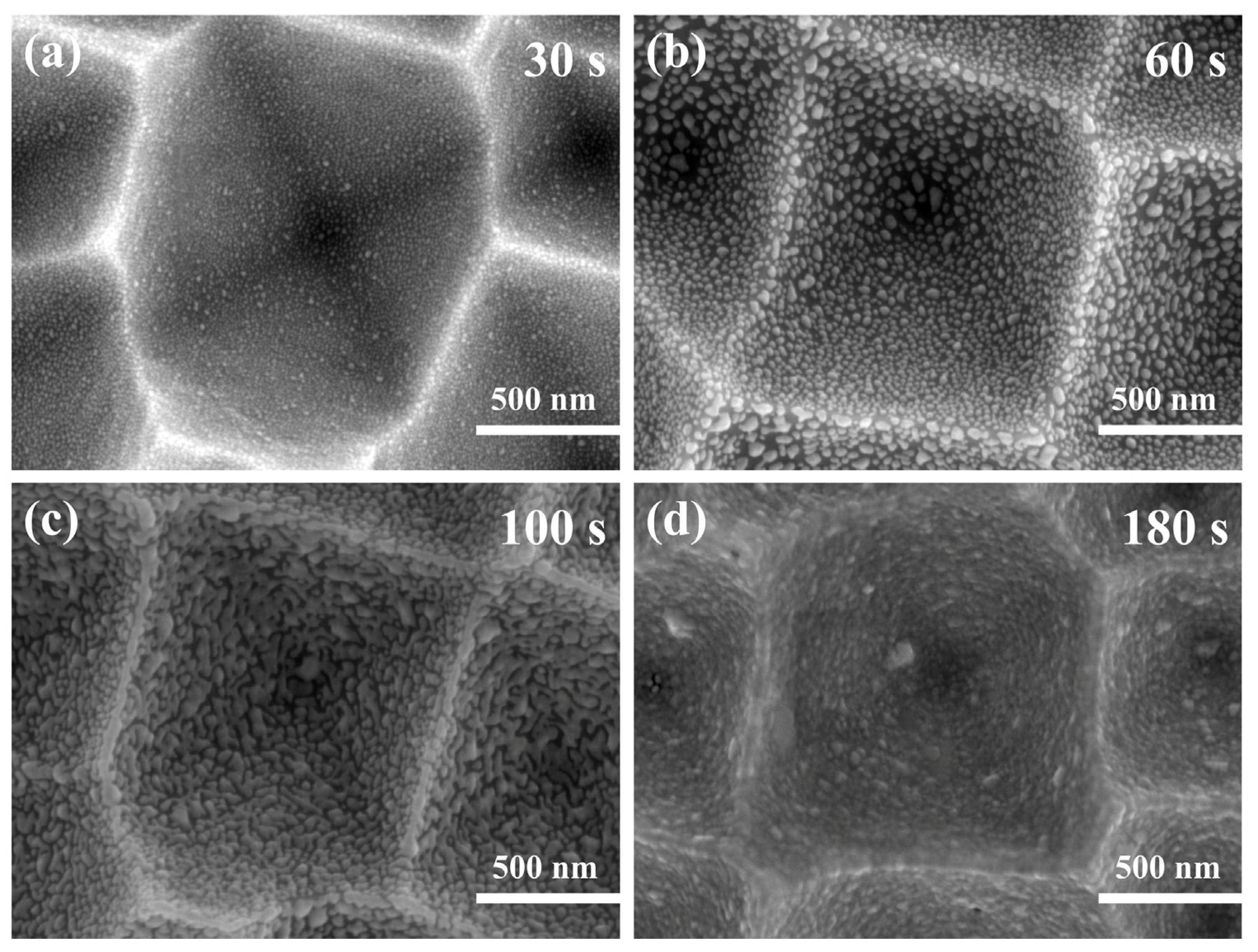
3.1. Evaluation of Silicon Inverted Pyramid

Figure 2 shows the surface morphology of the silicon wafer etched in different NH4HF2 solutions for 7 min. When the NH4HF2 concentration was 0.3 M, the Si surface was covered by a shallow crater structure and the sidewall edges were blurred (Figure 2a). With increasing NH4HF2 concentrations (0.5 M), the shallow crater structure on the silicon surface transformed into a large-scale, randomly distributed, inverted pyramidal structure with a size and depth of approximately 1 μm (Figure 2b). Further increasing the NH4HF2 concentration led to polished surfaces on the silicon wafer surface; the etched structure was no longer uniform, a large number of small-sized inverted pyramids were interspersed between the large-sized inverted pyramid structures, and the side edges became blurred (Figure 2c). When the concentration reached 0.9 M, one face of the wafer was completely converted into a polished surface with a flatter surface, as illustrated in Figure 2d. The reflectance of silicon wafers etched with different concentrations of NH4HF2 is shown in Figure S1. When the NH4HF2 concentration was 0.5 M, the reflectivity of the silicon wafer was the lowest. Hence, we concluded that the concentration of NH4HF2 in the etching solution system should be 0.5 M.
Figure 3 shows the SEM images and reflectance spectra of the samples etched with different concentrations of H2O2 solution at 0.5 M NH4HF2 for 7 min. When the concentration of H2O2 was 0.98 M, the wafer surface was filled with small pits and only a small area of the wafer surface had an evident inverted pyramid structure, as shown in Figure 3a. The overall structure was slightly improved as the H2O2 concentration was raised (Figure 3b). After the H2O2 concentration increased to 2.55 M, the silicon inverted pyramids were relatively uniformly distributed, the depth increased, and the four edges became clearly visible (Figure 3c–e). The reflectance spectra corresponded to the SEM images (Figure 2f), and the wafer etched with a low concentration of H2O2 (0.98–1.76 M) had a poor structure and higher reflectance, while the wafer etched with a high concentration of H2O2 (2.55–4.11 M) had a uniform structure and lower reflectance. The changes in reflectivity were less significant when the H2O2 concentration was 2.55–4.11 M.
When the concentration of H2O2 as an oxidizer was too low, it failed to provide enough holes to oxidize the surface, resulting in a significant decrease in the etching uniformity and etching rate of NH4HF2 and a large number of small inverted pyramids. PVP adsorbed on the silicon surface, resulting in a certain effective concentration of H2O2 touching the silicon surface, which inhibited the oxidation reaction. Therefore, increasing the concentration of H2O2 did not have a notable effect on the inverted pyramid structure. In conclusion, 2.55 M of H2O2 was sufficient for the experiment.
Furthermore, PVP was necessary to form the inverted pyramid structure. The surface of the wafer became brighter and flatter upon immersing it in the PVP-free etch solution for 7 min. As seen in Figure 4a, the average reflectivity of the etched wafer reached 48.72%, which was higher than that of the primary polished wafer (46%). Figure 4b shows the reflectance spectra of the silicon etched with different concentrations of PVP. As shown in Figure 4b, the reflectance spectra showed an ascent after an initial decline trend with the increase in the PVP concentration. The average reflectivity was low when the PVP concentration was in the range of 154–308 nM, and the optimal anti-reflection performance of the wafer was achieved at a concentration of 308 nM. Considering this balance, we selected the PVP of 308 nM for the subsequent study.
Figure 5 shows the SEM images etched at different AgNO3 concentrations for 7 min. When the concentration of AgNO3 was low (0.14 mM), the silicon surface was covered with small-sized inverted pyramids, as shown in Figure 5a. The size of the inverted pyramid structure was enlarged, the depth expanded, and the edges became visible when increasing the AgNO3 concentration. The overall structure of the inverted pyramid did not change dramatically when the AgNO3 content was at 0.24–0.42 mM, but the uniformity improved and the proportion of inverted pyramids below 1 μm decreased substantially (Figure 5b–e). Further increasing the AgNO3 concentration did not promote the formation of the inverted pyramid. It was easy to identify that the depth of the inverted pyramid became shallow and it also tended to form shallow craters (Figure 5f).
While the AgNO3 concentration was at 0.24–0.42 mM, the average reflectivity of the wafers was extremely similar (Figure S2). To better visualize the changes in the silicon surface morphology, ImageJ was applied to obtain metric statistics on the size and number of inverted pyramids, as illustrated in Figure 6. According to Figure 6a,f, it was apparently observed that the number of small-sized pyramids was 98% and 55% for low and high concentrations of AgNO3, respectively. Figure 6b–e show that the size distribution of the inverted pyramids was relatively even, especially in Figure 6d, where the size distribution was most concentrated, with a minimum relative standard deviation (RSD) of 26.19% and consistent with the Gaussian distribution. Therefore, 0.42 mM AgNO3 was selected for further experiments.
Figure S3 shows the SEM images of the silicon surface etched at different times. As illustrated in Figure S3a, the inverted pyramid structure fabricated at 3 min was evidently shallow, the four side edges of the inverted pyramid were blurred, and the structure size uniformity was poor. As the etching time increased, the size of the inverted pyramids became significantly larger (Figure S3b–d). On increasing the etching time, the average reflectivity descended to a stable level (Figure 7a). This indicates that a longer etching time does not further improve the anti-reflective properties of the wafer. In addition, the weight loss of the wafer was too severe for a long etch time, and the thickness of the wafer was less than one third of the original thickness after 15 min. The wafer became more brittle, which was not conducive to subsequent operations. Hence, we set a total of seven minutes as the most appropriate etching time.

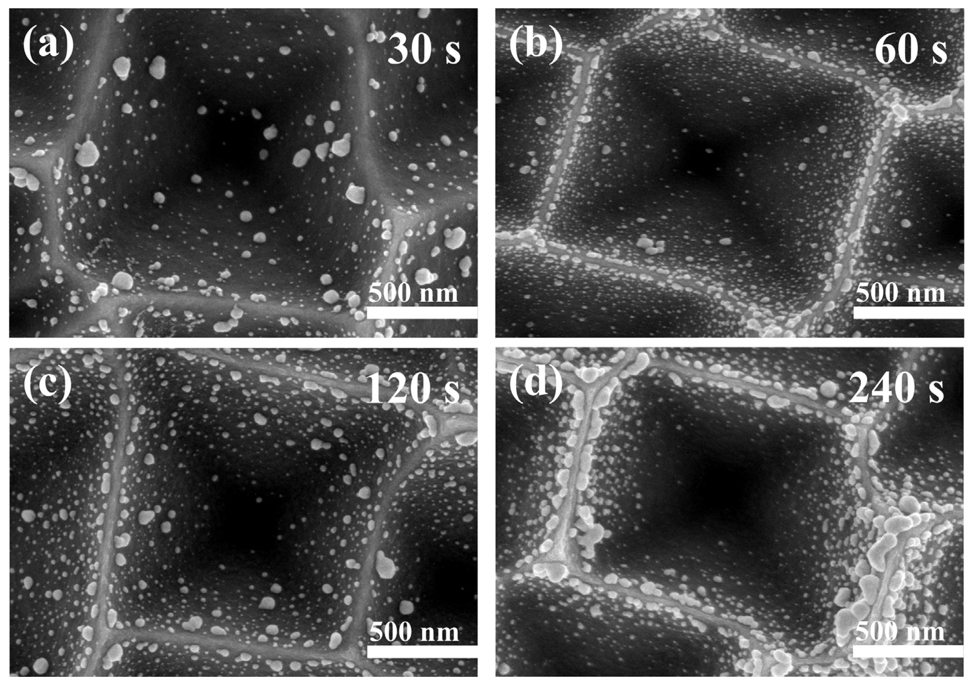
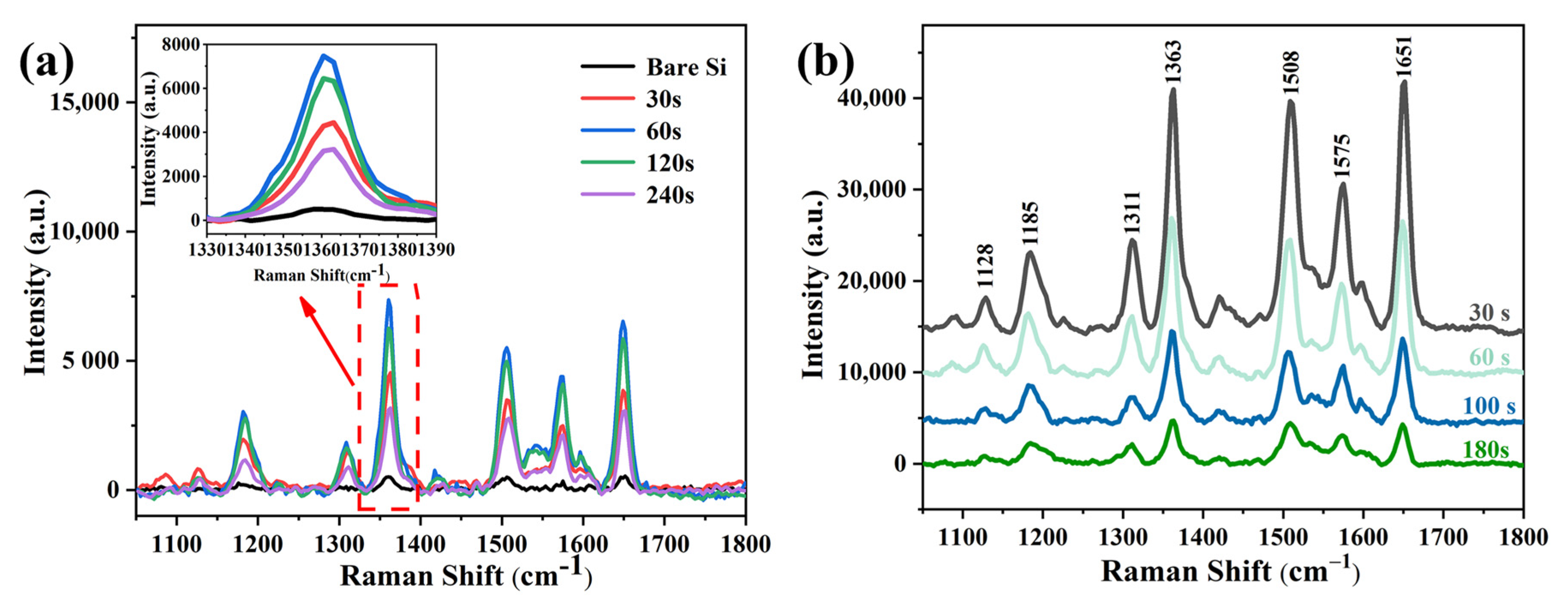
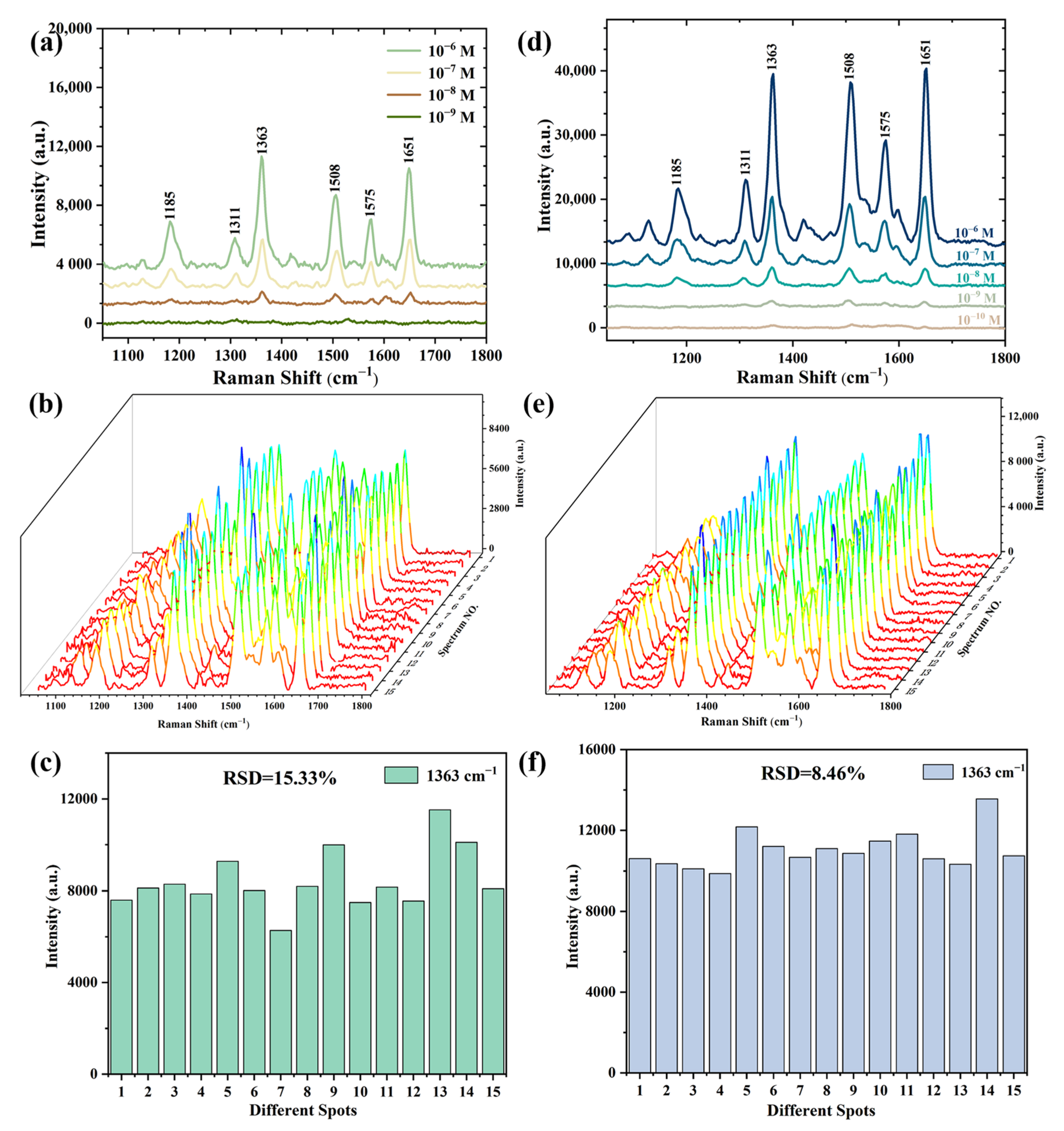
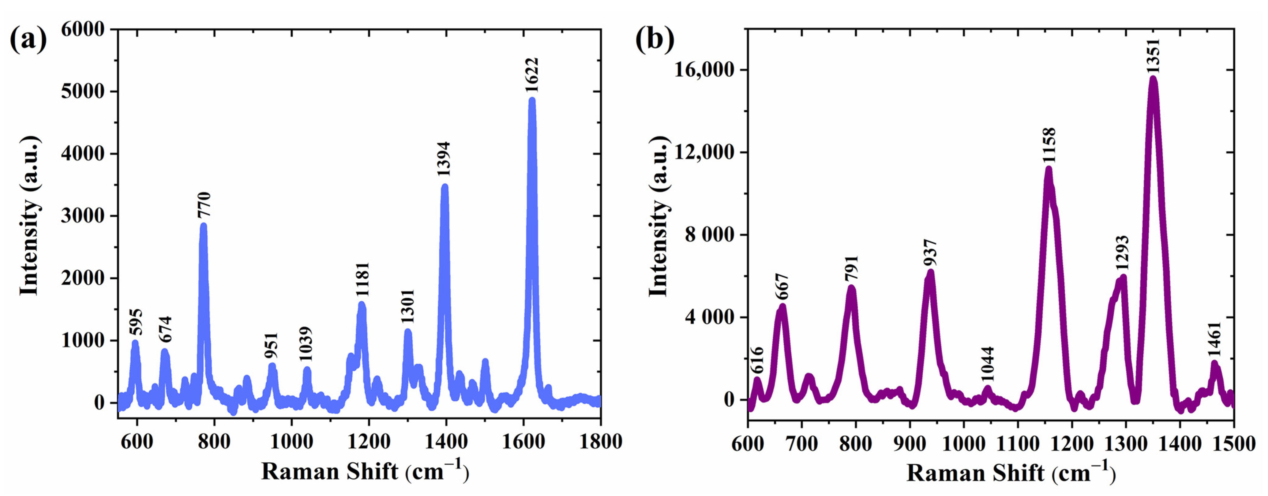
3.2. SERS Response from the Textured Surface

An aqueous solution of 0.5 M NH4HF2, 2.55 M H2O2, 308 nM PVP, and 0.42 mM AgNO3 was chosen for the experiment considering potential advantages in size uniformity and anti-reflection properties. The etching temperature was set to 65 °C and the total etching time was 7 min. The silicon inverted pyramids prepared with these parameters were subjected to the subsequent deposition of silver nanoparticles.
Regarding the SERS response, we focused on comparing the Raman peak intensities of silver nanoparticles on silicon surfaces at different deposition states using two different methods of depositing silver nanoparticles.
Figure 8 shows the SEM images of silver nanoparticles deposited at different times by electroless deposition. We identified that the silver nanoparticles were not easily deposited to the bottom of the inverted pyramid and the particle size gradually became smaller along the silicon wall. As the deposition time increased, the number of silver nanoparticles on the silicon surface was boosted, and the silver nanoparticles tended to undergo aggregation at the top of the silicon wall, transforming into nano-chain-like silver. Figure S4 shows the EDS spectrum of the substrate deposited with 240 s of Ag NPS, confirming the presence of only three elements, C, Si, and Ag, which proves that no other elements were present in the Ag nanoparticles.
Figure 9 shows SEM images of silver nanoparticles sputtered on silicon inverted pyramids with a radiofrequency sputtering system at different times. When the sputtering time was 30 s, the silver nanoparticles were deposited regularly on the silicon inverted pyramids, without aggregation or excessive spacing. The size and spacing of the silver nanoparticles were 8–20 nm and 5–10 nm, respectively (Figure 9a). After extending the sputtering time to 60 s, the size of the silver nanoparticles ranged from 10 to 45 nm, and the majority of them were above 20 nm. Meanwhile, it was evident that the distance between the particles became more significant (Figure 9b). Upon continuing to increase the time, the silver nanoparticles gradually transformed into networked silver (Figure 9c) and became a silver film at a sputtering time of 180 s (Figure 9d). Figure S5 illustrates the EDS spectrum of the substrate sputtered with Ag NPs for 30 s, showing the presence of only three elements, O, Si, and Ag, which proved that no other elements were present in the Ag nanoparticles. Silver nanoparticles and silicon are easily oxidized in air, resulting in the presence of the O element.
Figure 10a shows the Raman spectra of 0.1 M R6G tested on bare silicon and 1.0 × 10⁻⁶ M R6G measured on silicon inverted pyramid SERS substrates after depositing Ag NPs by electroless deposition for different times. The Raman peak positions of R6G have been labeled at 1128, 1185, 1311, 1363, 1508, 1575, and 1651 cm−1, which are consistent with the previously reported peak positions [34]. The 1128, 1182 cm−1 SERS peaks are attributed to C-H in-plane bending. The SERS peaks at 1311 cm−1 can be attributed to N-N in-plane bending vibration, while the SERS peaks at 1363, 1508, 1575, and 1651 cm−1 are all due to aromatic C-C stretching vibration [35]. It can be clearly seen that all the SERS substrates show high-intensity Raman peaks compared to bare silicon, which proves the feasibility of silicon inverted pyramid/Ag NPs as SERS substrates. In addition, considering that the most dominant peak was around 1363 cm−1, this peak was chosen to compare the SERS performance of different substrates.
As the depositing time increased from 30 to 60 s, the intensity also surged. This was due to the increase in the number of silver nanoparticles deposited on the silicon walls, which reduced the gap between the particles, strengthening the electric-field enhancement and the associated hot spots. After increasing the deposition time to 120 s, the intensity of the peaks only slightly decreased, which was consistent with the similar results in the SEM images. Nevertheless, at the deposition time of 240 s, a significant decrease in the intensity of the peak at 1363 cm−1 could be observed. Due to the aggregation of isolated nanoparticles into silver nanostrands with increasing time, the size and spacing of the silver nanoparticles increased considerably, making it difficult to generate strong electric-field coupling and reducing the Raman peak intensity. Thus, a deposition time of 60 s was set as the ideal parameter for optimal substrate SERS performance.
Figure 10b shows the SERS spectra of 10−6 M R6G molecules of the substrate after sputtering silver nanoparticles at different times. As illustrated, the intensity of the peak gradually becomes weaker as the sputtering time increases. This is due to the longer sputtering time, which hampers the formation of silver nanoparticles with a smaller size and spacing at the silicon wall, weakening the electric-field enhancement and the associated hot spots. Nevertheless, the substrates prepared by the radiofrequency sputtering system show superior SERS performance compared to those prepared by electroless deposition. Furthermore, the intensity of the peak at 1363 cm−1 of the substrates sputtered for 30 s was considerably higher than that of the substrates prepared by the optimal electroless deposition (60 s). This is because the radiofrequency sputtering system can build smaller and denser silver nanoparticles compared with electroless deposition, solving the issue of electroless deposition of silver nanoparticles that cannot be easily deposited at the bottom of the inverted pyramidal silicon wall and tend to accumulate at the top.
High sensitivity and reproducibility are crucial for an excellent SERS substrate. Therefore, the SERS substrates prepared by different methods were tested for their limit concentration and reproducibility, respectively, and the results are shown in Figure 11. Figure 11a shows the Raman spectra of various R6G concentrations (10−6~10−9 M) collected from the substrates prepared by electroless deposition; the lowest detectable concentration reaches 10−8 M. To evaluate the reproducibility for the SERS signals, Raman spectra of the 10−6 M R6G were collected from 15 different points on the substrates (Figure 11b). Figure 11c shows the peak intensities at 1363 cm−1 for R6G with a concentration of 10−6 M from 15 different points on the SERS substrate prepared by electroless deposition, and the relative standard deviation (RSD) was calculated to be 15.33%. Sensitivity and repeatability tests and calculations were also conducted for the substrates prepared by radiofrequency sputtering, and the results are shown in Figure 11d,e. This result demonstrates that the detection limit of a substrate prepared by sputtering for 30 s for the R6G solution can reach 10−10 M. The Raman signal of 10−7 M R6G on the substrate was collected and the results indicate higher reproducibility with an RSD of 8.46%.
To intuitively evaluate the SERS effects of different substrates, the enhancement factor (EF) can be expressed by calculating the following Equation (1):
E F = I S E R S × N R S I R S × N S E R S
where ISERS and IRS are the peak intensities at 1363 cm−1 for R6G obtained from SERS spectra and normal Raman spectra, respectively. NSERS and NRS are the numbers of R6G molecules excited by the laser beam on the SERS substrate and bare silicon wafer, respectively. Therefore, the EF values of the SERS substrates prepared by electroless deposition and radiofrequency sputtering were 1.68 × 10⁶ and 2.21 × 10⁷, respectively. The value for the SERS substrate fabricated by radiofrequency sputtering is 13.07 times higher than that of electroless deposition.
In addition, to verify the general sensitivity to other organic molecules, we also selected MB and AMX molecules to detect on the substrates, which were prepared by sputtering silver nanoparticles on Si-inverted pyramids. Figure 12a,b shows the Raman spectra of 10−5 M MB solution and 10−4 M AMX solution collected on the SERS substrate sputtered with 30 s silver nanoparticles, respectively. For comparison, the normal Raman spectra of 1 mM MB and 0.01 M AMX on bare silicon were also collected for each one (Figure S6a,b). All characteristic distinguishable peaks of MB positioned at 595, 674, 770, 951, 1039, 1181, 1301, 1394, and 1622 cm−1 and AMX positioned at 616, 667, 791, 937, 1158, 1293, 1351, and 1461 cm−1 were observed, which are in good agreement with previously reported values, and the characteristic peaks are greatly enhanced compared to normal Raman spectra. The corresponding vibration mode attributed to each Raman peak for both analytes is provided in Tables S1 and S2. In this study, only the effect of different silver nanoparticle deposition states on SERS was investigated, leaving room for further examinations focused on the effect of different sizes of inverted pyramids on the performance of SERS substrates.

4. Conclusions

We prepared silicon inverted pyramids with excellent anti-reflectivity and uniform sizes by Ag@PVP-ACE. The significant Raman enhancement of R6G by silicon inverted pyramid/Ag NPs as SERS substrates was demonstrated. Comparing the Raman enhancement effects of SERS substrates in different silver nanoparticle deposition states, our most important outcomes showed that silver nanoparticles that are smaller and more densely distributed lead to the formation of substrates with higher sensitivity. The silicon inverted pyramid/Ag NPs prepared in this study exhibit a similar size and structure with a denser distribution of inverted pyramids compared to commercial Klarite SERS samples, as well as other advantageous features, e.g., lower costs, which are extremely beneficial for practical applications of SERS substrates.

Supplementary Materials

The following supporting information can be downloaded at: https://www.mdpi.com/article/10.3390/ma16103634/s1.

Author Contributions

Conceptualization, investigation, formal analysis, data curation, and writing—review and editing, J.L.; methodology, formal analysis, and data curation, Y.Y.; formal analysis, Z.Z.; methodology, Y.L.; project administration, methodology, J.G.; supervision, project administration, funding acquisition, and writing—review and editing, Z.G. All authors have read and agreed to the published version of the manuscript.

Funding

This work was supported by funding from the National Natural Science Foundation of China (project No. 51902157) and the Priority Academic Program Development of Jiangsu Higher Education Institutions (PAPD).

Informed Consent Statement

Informed consent was obtained from all subjects involved in the study.

Data Availability Statement

Not applicable.

Acknowledgments

This work was supported by funding from the Jiangsu Collaborative Innovation Center for Advanced Inorganic Function Composites, the National Natural Science Foundation of China (project No. 51902157), the Innovation and Entrepreneurship Talent Program of Jiangsu Province, China, the Priority Academic Program Development of Jiangsu Higher Education Institutions (PAPD), Nanjing Naxin New Material Co., Ltd. (Nanjing, Jiangsu, China).

Conflicts of Interest

The authors declare that they have no known competing financial interests or personal relationships that could have appeared to influence the work reported in this paper.

References

  1. Chang, T.; Chuang, K.; Chang, Y. Ag/Ga-doped ZnO/pyramidal Silicon as a Multifunctional Surface-Enhanced Raman Scattering Substrate. J. Alloys Compd. 2022, 893, 162288. [Google Scholar] [CrossRef]
  2. Fan, M.; Andrade, G.F.S.; Brolo, A.G. A Review On the Fabrication of Substrates for Surface Enhanced Raman Spectroscopy and their Applications in Analytical Chemistry. Anal. Chim. Acta 2011, 693, 7–25. [Google Scholar] [CrossRef] [PubMed]
  3. Langer, J.; de Aberasturi, D.J.; Aizpurua, J.; Alvarez-Puebla, R.A.; Auguie, B.; Baumberg, J.J.; Bazan, G.C.; Bell, S.E.J.; Boisen, A.; Brolo, A.G.; et al. Present and Future of Surface-Enhanced Raman Scattering. ACS Nano 2020, 14, 28–117. [Google Scholar] [CrossRef] [PubMed]
  4. Mikac, L.; Sabolic, N.; Raic, M.; Maric, I.; Jurkin, T.; Gotic, M.; Skrabic, M.; Rigo, I.; Veres, M.; Ivanda, M. Synthesis of Porous Silicon Based Nanoparticles for Applications in Surface Enhanced Raman Spectroscopy. Vacuum 2021, 191, 110335. [Google Scholar] [CrossRef]
  5. Lin, Z.; He, L. Recent Advance in SERS Techniques for Food Safety and Quality Analysis: A Brief Review. Curr. Opin. Food Sci. 2019, 28, 82–87. [Google Scholar] [CrossRef]
  6. Wei, Y.; Zhu, Y.; Wang, M. Surface-Enhanced Raman Spectroscopy of Gastric Cancer Serum with Gold Nanoparticles/Silicon Nanowire Arrays. Optik 2016, 127, 7902–7907. [Google Scholar] [CrossRef]
  7. Arzumanyan, G.; Doroshkevich, N.; Mamatkulov, K.; Shashkov, S.; Girel, K.; Bandarenka, H.; Borisenko, V. Phospholipid Detection by Surface-Enhanced Raman Scattering Using Silvered Porous Silicon Substrates. Phys. Status Solidi A 2017, 214, 1600915. [Google Scholar] [CrossRef]
  8. Ding, S.; You, E.; Tian, Z.; Moskovits, M. Electromagnetic Theories of Surface-Enhanced Raman Spectroscopy. Chem. Soc. Rev. 2017, 46, 4042–4076. [Google Scholar] [CrossRef]
  9. Xu, H.X.; Aizpurua, J.; Kall, M.; Apell, P. Electromagnetic Contributions to Single-Molecule Sensitivity in Surface-Enhanced Raman Scattering. Phys. Rev. E 2000, 62, 4318–4324. [Google Scholar] [CrossRef]
  10. Zhang, B.; Wang, H.; Lu, L.; Ai, K.; Zhang, G.; Cheng, X. Large-Area Silver-Coated Silicon Nanowire Arrays for Molecular Sensing Using Surface-Enhanced Raman Spectroscopy. Adv. Funct. Mater. 2008, 18, 2348–2355. [Google Scholar] [CrossRef]
  11. Shinki; Singh, J.; Sarkar, S. Tuning the Topographical Parameters of Si Pyramids for a Better Surface Enhanced Raman Response. Phys. Chem. Chem. Phys. 2021, 23, 26407–26416. [Google Scholar] [CrossRef]
  12. Chang, T.; Chang, Y.; Chen, C.; Chuang, K.; Chou, C. A Facile Method to Directly Deposit the Large-Scale Ag Nanoparticles On a Silicon Substrate for Sensitive, Uniform, Reproducible and Stable SERS Substrate. J. Alloys Compd. 2019, 782, 887–892. [Google Scholar] [CrossRef]
  13. Lu, G.; Wang, G.; Li, H. Effect of Nanostructured Silicon On Surface Enhanced Raman Scattering. RSC Adv. 2018, 8, 6629–6633. [Google Scholar] [CrossRef]
  14. Wang, G.; Yi, R.; Zhai, X.; Bian, R.; Gao, Y.; Cai, D.; Liu, J.; Huang, X.; Lu, G.; Li, H.; et al. A Flexible SERS-active Film for Studying the Effect of Non-Metallic Nanostructures On Raman Enhancement. Nanoscale 2018, 10, 16895–16901. [Google Scholar] [CrossRef]
  15. Shinki; Sarkar, S. Is 3D Surface Structuring Always a Prerequisite for Effective SERS? Surf. Interfaces 2022, 33, 102223. [Google Scholar] [CrossRef]
  16. Akbiyik, A.; Avishan, N.; Demirtas, O.; Demir, A.K.; Yuce, E.; Bek, A. Laser Photochemical Nanostructuring of Silicon for Surface Enhanced Raman Spectroscopy. Adv. Opt. Mater. 2022, 10, 2200114. [Google Scholar] [CrossRef]
  17. Chen, J.; Martensson, T.; Dick, K.A.; Deppert, K.; Xu, H.Q.; Samuelson, L.; Xu, H. Surface-Enhanced Raman Scattering of Rhodamine 6G On Nanowire Arrays Decorated with Gold Nanoparticles. Nanotechnology 2008, 19, 275712. [Google Scholar] [CrossRef]
  18. Mehrvar, L.; Sadeghipari, M.; Tavassoli, S.H.; Mohajerzadeh, S. Surface-Enhanced Raman Spectroscopy of Dye Molecules On Ag-modified Silicon Nanowire Substrates: Influence of Photoinduced Probe Degradation On Enhancement Factors. J. Raman Spectrosc. 2017, 48, 1171–1181. [Google Scholar] [CrossRef]
  19. Nguyen, T.V.; Vu, D.C.; Pham, T.S.; Bui, H.; Pham, T.B.; Hoang, T.H.C.; Pham, V.H.; Pham, V.H. Quasi-3D-Structured Surface-Enhanced Raman Scattering Substrates Based on Silver Nanoparticles/Mesoporous Silicon Hybrid. Phys. Status Solidi A 2022, 219, 2200128. [Google Scholar] [CrossRef]
  20. Mehrvar, L.; Sadeghipari, M.; Tavassoli, S.H.; Mohajerzadeh, S.; Fathipour, M. Optical and Surface Enhanced Raman Scattering Properties of Ag Modified Silicon Double Nanocone Array. Sci. Rep. 2017, 7, 12106. [Google Scholar] [CrossRef]
  21. Roy, A.; Maiti, A.; Chini, T.K.; Satpati, B. Annealing Induced Morphology of Silver Nanoparticles on Pyramidal Silicon Surface and their Application to Surface-Enhanced Raman Scattering. ACS Appl. Mater. Inter. 2017, 9, 34405–34415. [Google Scholar] [CrossRef]
  22. Golubewa, L.; Karpicz, R.; Matulaitiene, I.; Selskis, A.; Rutkauskas, D.; Pushkarchuk, A.; Khlopina, T.; Michels, D.; Lyakhov, D.; Kulahava, T.; et al. Surface-Enhanced Raman Spectroscopy of Organic Molecules and Living Cells with Gold-Plated Black Silicon. ACS Appl. Mater. Inter. 2020, 12, 50971–50984. [Google Scholar] [CrossRef] [PubMed]
  23. Zhang, C.; Man, B.Y.; Jiang, S.Z.; Yang, C.; Liu, M.; Chen, C.S.; Xu, S.C.; Qiu, H.W.; Li, Z. SERS Detection of Low-Concentration Adenosine by Silver Nanoparticles On Silicon Nanoporous Pyramid Arrays Structure. Appl. Surf. Sci. 2015, 347, 668–672. [Google Scholar] [CrossRef]
  24. Scholes, F.H.; Davis, T.J.; Vernon, K.C.; Lau, D.; Furman, S.A.; Glenn, A.M. A Hybrid Substrate for Surface-Enhanced Raman Scattering Spectroscopy: Coupling Metal Nanoparticles to Strong Localised Fields On a Micro-Structured Surface. J. Raman Spectrosc. 2012, 43, 196–201. [Google Scholar] [CrossRef]
  25. Vernon, K.C.; Davis, T.J.; Scholes, F.H.; Gomez, D.E.; Lau, D. Physical Mechanisms Behind the SERS Enhancement of Pyramidal Pit Substrates. J. Raman Spectrosc. 2010, 41, 1106–1111. [Google Scholar] [CrossRef]
  26. Xu, G.J.; Cheng, H.Y.; Jones, R.B.; Feng, Y.Q.; Gong, K.D.; Li, K.J.; Fang, X.Z.; Tahir, M.A.; Valev, V.K.; Zhang, L.W. Surface-Enhanced Raman Spectroscopy Facilitates the Detection of Microplastics < 1 Mu M in the Environment. Environ. Sci. Technol. 2020, 54, 15594–15603. [Google Scholar]
  27. Zhang, C.; Chen, L.; Zhu, Y.; Guan, Z. Fabrication of 20.19% Efficient Single-Crystalline Silicon Solar Cell with Inverted Pyramid Microstructure. Nanoscale Res. Lett. 2018, 13, 91. [Google Scholar] [CrossRef]
  28. Liu, Y.; Dong, K.; Bian, L.; Guan, Z. One-Step Fabrication of Inverted Pyramid Textured Silicon Wafers via Silver-Assisted Chemical Etching Combing with Synergism of Polyvinylpyrrolidone (PVP). Crystals 2021, 11, 459. [Google Scholar] [CrossRef]
  29. Gu, H.; Guan, Z.; Liu, Y. Large-Scale Preparation of 22.06% Efficiency Single-Crystalline Silicon Solar Cells with Inverted Pyramid Microstructure through Nanostructure Rebuilding Treatment. Mater. Res. Express. 2020, 7, 096203. [Google Scholar] [CrossRef]
  30. Wu, J.T.; Liu, Y.P.; Chen, W.; Zhao, Y.; Chen, Q.S.; Tang, H.B.; Wang, Y.; Du, X.L. Influence of Different-Sized Inverted-Pyramids of Silicon Texture by Ag Manipulation On Solar Cell Performance. Appl. Surf. Sci. 2020, 506, 144778. [Google Scholar] [CrossRef]
  31. Assisted, L.; Rani, S.; Shukla, A.K. Investigation of Silver Decorated Silicon Nanowires as Ultrasensitive and Cost-Effective Surface-Enhanced Raman Substrate. Thin Solid Films 2021, 723, 138595. [Google Scholar]
  32. Hildebrandt, P.; Stockburger, M. Surface-Enhanced Resonance Raman Spectroscopy of Rhodamine 6G Adsorbed On Colloidal Silver. J. Phys. Chem. 1984, 88, 5935–5944. [Google Scholar] [CrossRef]
  33. Anastasopoulos, J.A.; Soto Beobide, A.; Manikas, A.C.; Voyiatzis, G.A. Quantitative Surface-Enhanced Resonance Raman Scattering Analysis of Methylene Blue Using Silver Colloid. J. Raman Spectrosc. 2017, 48, 1762–1770. [Google Scholar] [CrossRef]
  34. Watanabe, H.; Hayazawa, N.; Inouye, Y.; Kawata, S. DFT Vibrational Calculations of Rhodamine 6G Adsorbed On Silver: Analysis of Tip-Enhanced Raman Spectroscopy. J. Phys. Chem. B 2005, 109, 5012–5020. [Google Scholar] [CrossRef]
  35. Chang, T.; Chuang, K.; Chang, Y.; Chou, C. Optimizing and Improving the Growth of Ag Nanoparticles Decorated On the Silicon Pyramid for Surface-Enhanced Raman Spectroscopy. Mater. Chem. Phys. 2022, 280, 125823. [Google Scholar] [CrossRef]
Figure 1. Schematic procedure for the fabrication of silicon inverted pyramid/Ag NPs.
Materials 16 03634 g001
Figure 2. SEM images of Si surface and cross-section etched in different NH4HF2 solutions for 7 min: (a) 0.3 M; (b) 0.5 M; (c) 0.7 M; (d) 0.9 M.
Materials 16 03634 g002
Figure 3. SEM images of Si surface etched in different H2O2 solutions for 7 min: (a) 0.98 M; (b) 1.76 M; (c) 2.55 M; (d) 3.33 M; (e) 4.11 M. (f) Reflectance spectra.
Materials 16 03634 g003
Figure 4. Reflectance spectra of etching systems etched for 7 min (a) without PVP and (b) with different concentrations of PVP.
Materials 16 03634 g004
Figure 5. SEM images of Si surface etched in different AgNO3 solutions for 7 min: (a) 0.14 mM; (b) 0.24 mM; (c) 0.33 mM; (d) 0.42 mM; (e) 0.52 mM; (f) 0.62 mM.
Materials 16 03634 g005
Figure 6. Histograms of inverted pyramid pore size distribution etched with different AgNO3 concentrations: (a) 0.14 mM; (b) 0.24 mM; (c) 0.33 mM; (d) 0.42 mM; (e) 0.52 mM; (f) 0.62 mM.
Materials 16 03634 g006
Figure 7. (a) Reflectance spectra and (b) thickness variation of silicon wafers etched for different times.
Materials 16 03634 g007
Figure 8. SEM images of substrates immersed in AgNO3/HF (0.5 mM AgNO3, 9% HF) aqueous solution for different times at room temperature: (a) 30 s; (b) 60 s; (c) 120 s; (d) 240 s.
Materials 16 03634 g008
Figure 9. SEM images with magnetron sputtering at different times: (a) 30 s; (b) 60 s; (c) 100 s; (d) 180 s.
Materials 16 03634 g009
Figure 10. Raman spectra of R6G measured on SERS substrates prepared with (a) different Ag deposition times and (b) different Ag sputtering times.
Materials 16 03634 g010
Figure 11. (a) The Raman spectra of various concentrations of R6G solution; (b) Raman spectra of 10−6 M R6G solution from 15 random points; (c) intensity of the characteristic peak at 1363 cm−1 from 15 random points on SERS substrates prepared by electroless deposition for 60 s; (d) the Raman spectra of various concentrations of R6G solution; (e) Raman spectra of 10−7 M R6G solution from 15 random points; (f) intensity of the characteristic peak at 1363 cm−1 from 15 random points on SERS substrates prepared by sputtering for 30 s.
Materials 16 03634 g011
Figure 12. Raman spectra of (a) MB (1.0 × 10⁻⁵ M) and (b) AMX (1.0 × 10⁻⁴ M) were collected on a substrate (silver sputtering time of 30 s on Si-inverted pyramid).
Materials 16 03634 g012
Disclaimer/Publisher’s Note: The statements, opinions and data contained in all publications are solely those of the individual author(s) and contributor(s) and not of MDPI and/or the editor(s). MDPI and/or the editor(s) disclaim responsibility for any injury to people or property resulting from any ideas, methods, instructions or products referred to in the content.

