
A Study of Defects in InAs/GaSb Type-II Superlattices Using High-Resolution Reciprocal Space Mapping

 , , ,
, , ,
Abstract
:1. Introduction
2. Materials and Methods
3. Results and Discussion
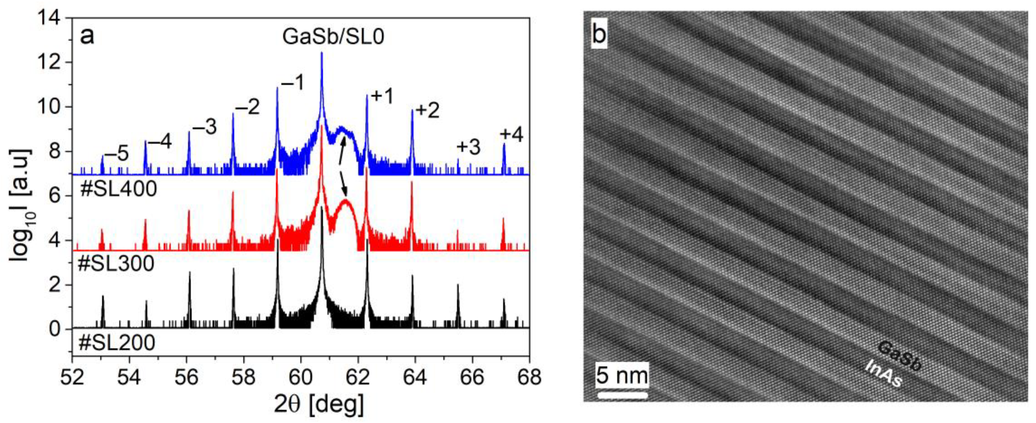
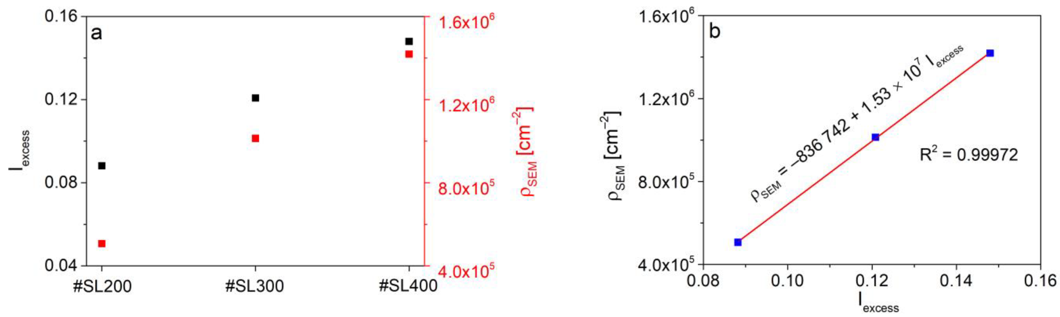
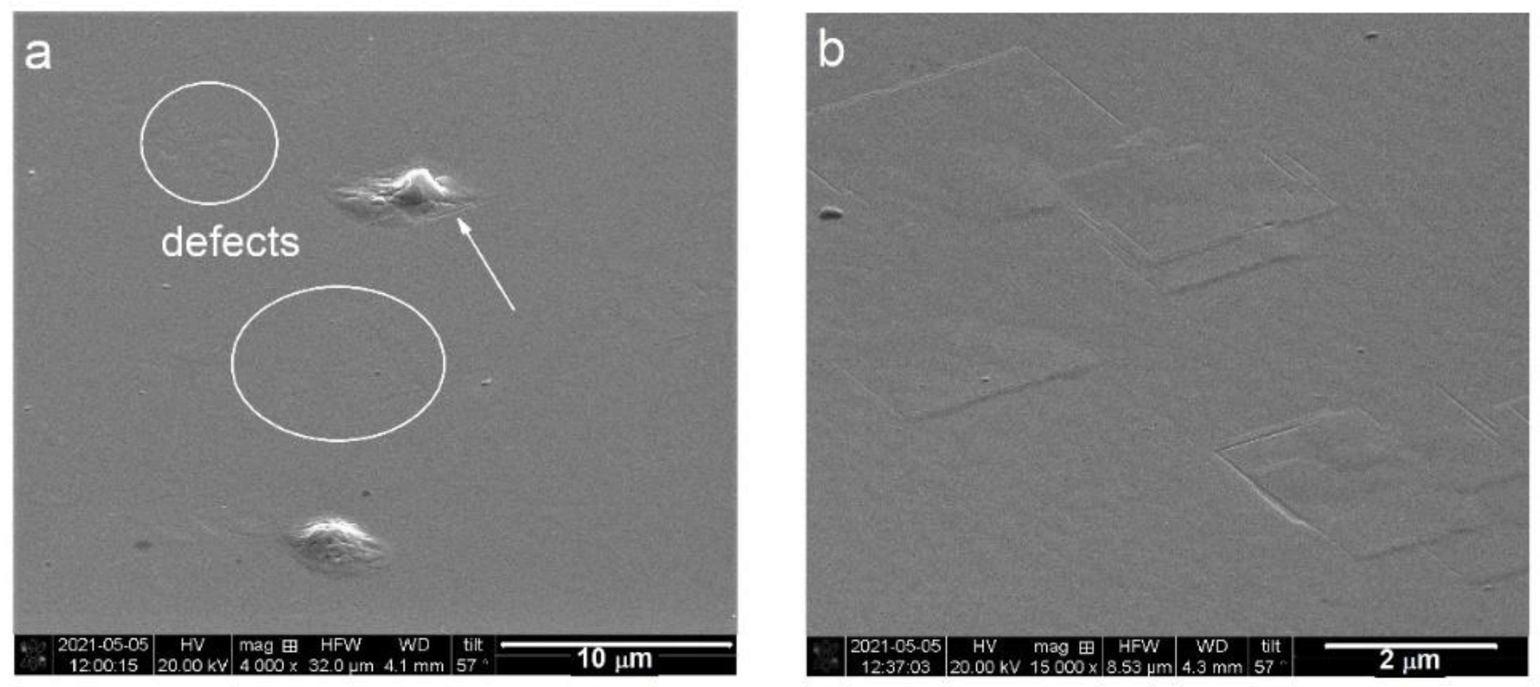
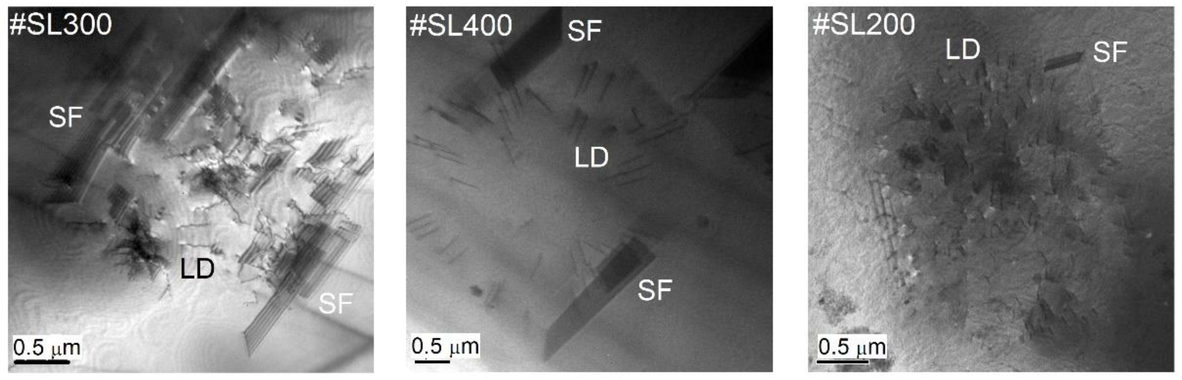
3.1. Simple Defect Analysis
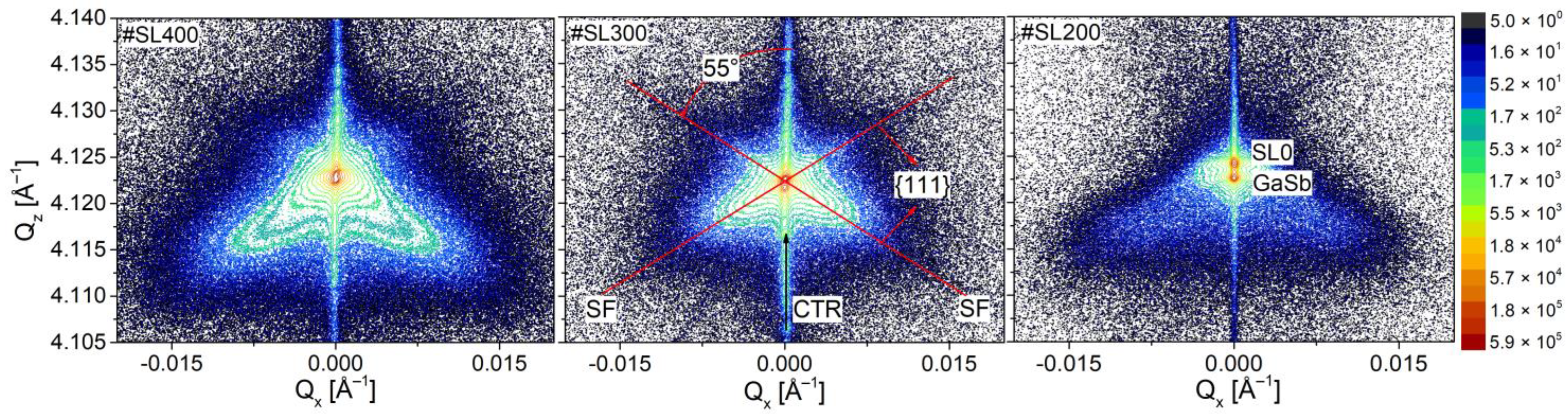
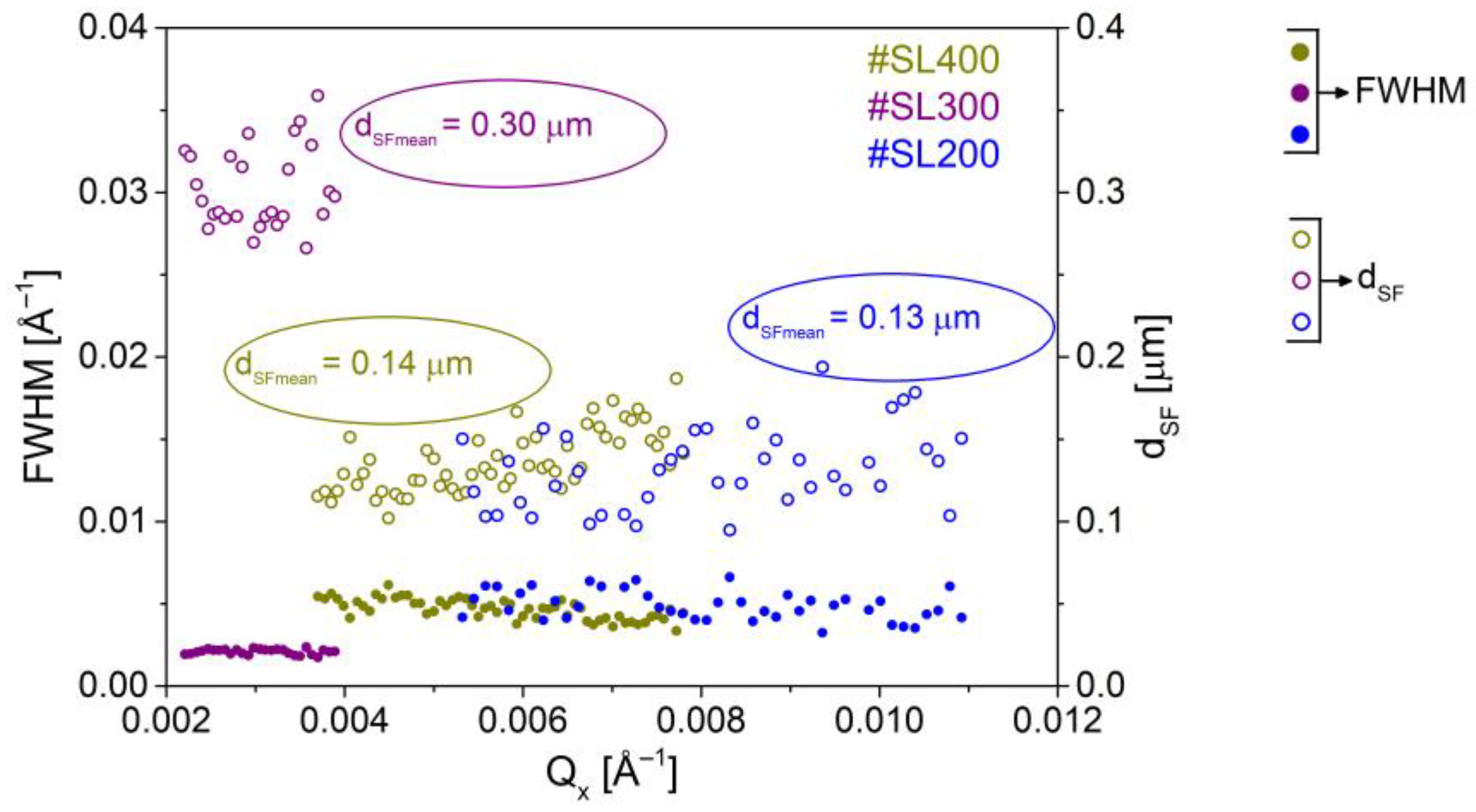
3.2. Detailed Defect Analysis
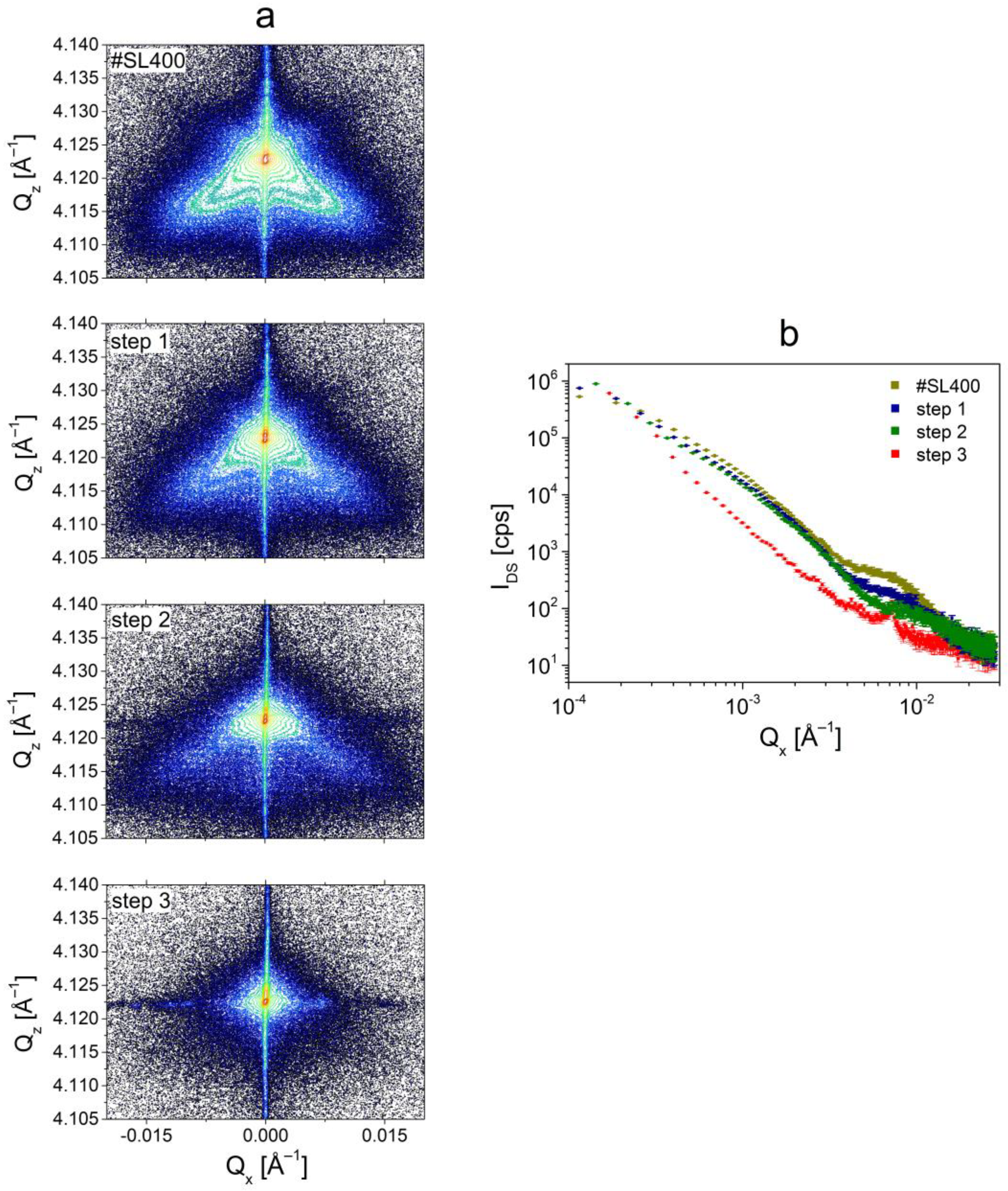
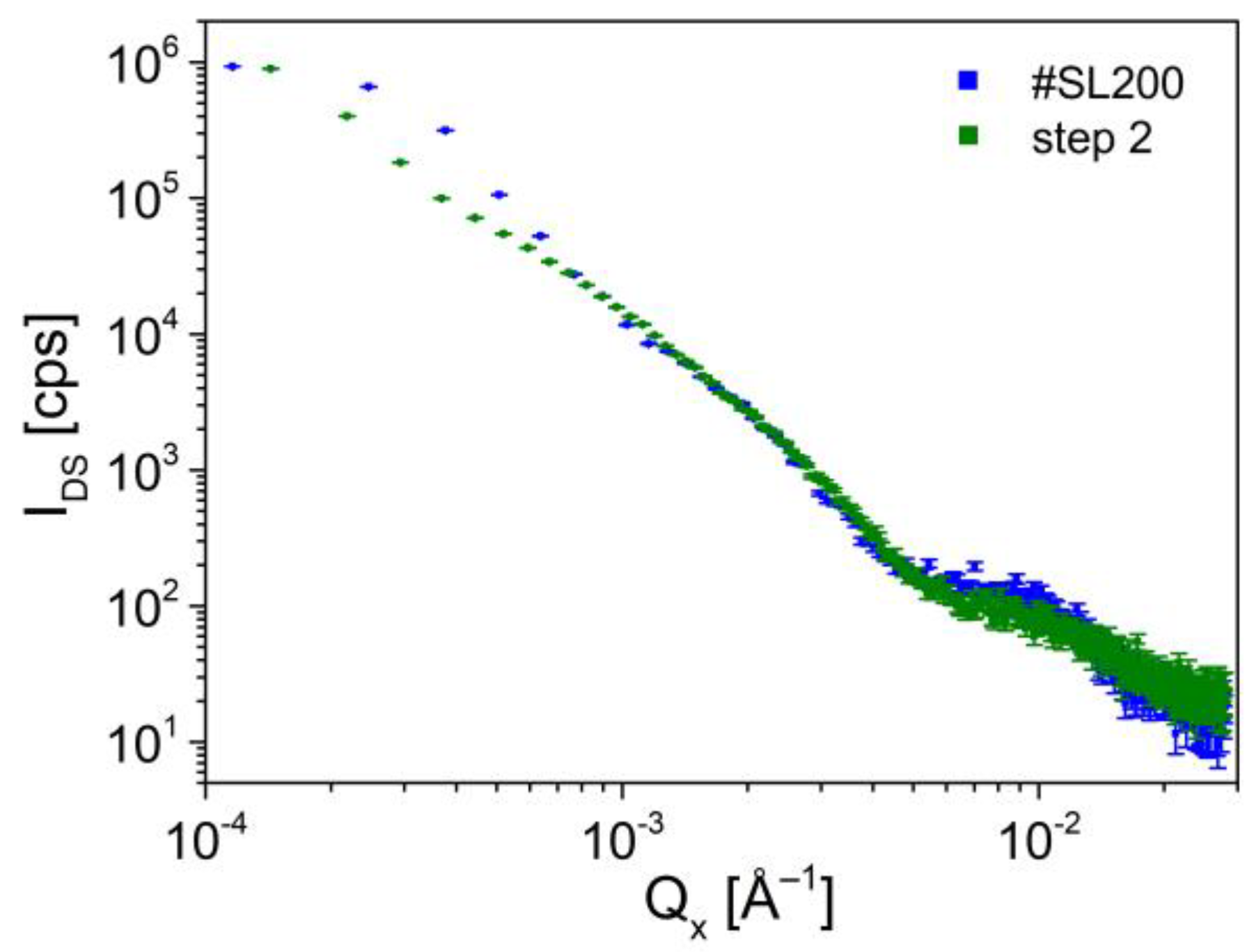
3.3. Analysis of the In-Depth Distribution of Defects
4. Conclusions
Author Contributions
Funding
Institutional Review Board Statement
Informed Consent Statement
Data Availability Statement
Conflicts of Interest
References
- Hirsch, P.B. Dislocations in semiconductors. Mater. Sci. Technol. 1985, 1, 666–677. [Google Scholar] [CrossRef]
- Jasik, A.; Ratajczak, J.; Sankowska, I.; Wawro, A.; Smoczyński, D.; Czuba, K. LT-AlSb Interlayer as a Filter of Threading Dislocations in GaSb Grown on (001) GaAs Substrate Using MBE. Crystals 2019, 9, 628. [Google Scholar] [CrossRef] [Green Version]
- Meduna, M.; Kreiliger, T.; Mauceri, M.; Puglisi, M.; Mancarella, F.; La Vis, F.; Crippa, D.; Miglio, L.; von Kanel, H. X-ray diffraction on stacking faults in 3C-SiC epitaxial microcrystals grown on patterned Si(0 0 1) wafers. J. Cryst. Growth 2019, 507, 70–76. [Google Scholar] [CrossRef]
- Lee, L.Y.; Frentrup, M.; Vacek, P.; Kappers, M.J.; Wallis, D.J.; Oliver, R.A. Investigation of stacking faults in MOVPE-grown zincblende GaN by XRD and TEM. J. Appl. Phys. 2019, 125, 105303. [Google Scholar] [CrossRef]
- Mahajan, S. Defects in semiconductors and their effects on devices. Acta Mater. 2000, 48, 137–149. [Google Scholar] [CrossRef]
- Czuba, K.; Sankowska, I.; Jureńczyk, J.; Jasik, A.; Papis-Polakowska, E.; Kaniewski, J. Influence of Be doping placement in InAs/GaSb superlattice-based absorber on the performance of MWIR photodiodes. Semicond. Sci. Technol. 2017, 320, 55010. [Google Scholar] [CrossRef]
- Balakrishnan, G.; Rotter, T.J.; Ahirwar, P.; Clark, S.P.; Patel, V.; Albrecht, A.; Hains, C.P.; Lai, Y.-Y.; Wang, T.L.; Yarborough, J.M.; et al. Lattice mismatched growth for mid-IR VECSELs. Proc. SPIE 2011, 7919, 79190G. [Google Scholar] [CrossRef]
- Sai-Halasz, G.A.; Tsu, R.; Esaki, L. A new semiconductor superlattice. Appl. Phys. Lett. 1977, 30, 651–653. [Google Scholar] [CrossRef]
- Plis, E.A. InAs/GaSb type-II superlattice detectors. Adv. Electron. 2014, 2014, 246769. [Google Scholar] [CrossRef] [Green Version]
- Rogalski, A.; Martyniuk, P.; Kopytko, M. InAs/GaSb type-II superlattice infrared detectors: Future prospect. Appl. Phys. Rev. 2017, 4, 031304. [Google Scholar] [CrossRef]
- Razegi, M. 9- InAs/GaSb type II superlattices: A developing material system for third generation of IR imaging. In Woodhead Publishing Series in Electronic and Optical Materials, Mid-Infrared Optoelectronics; Woodhead Publishing: Sawston, UK, 2020; pp. 379–413. [Google Scholar] [CrossRef]
- Rodriguez, J.B.; Christol, P.; Cerutti, F.; Chevrier, F.; Joullie, A. MBE growth and characterization of type-II InAs/GaSb superlattices for mid-infrared detection. J. Cryst. Growth 2005, 274, 6–13. [Google Scholar] [CrossRef]
- Ye, H.; Li, L.; Hinkey, R.T.; Yang, R.Q.; Mishima, T.D.; Keay, J.C.; Santos, M.B.; Johnson, M.B. MBE growth optimization of InAs (001) homoepitaxy. J. Vac. Sci. Technol. B 2013, 31, 03C135. [Google Scholar] [CrossRef]
- Jasik, A.; Sankowska, I.; Wawro, A.; Ratajczak, J.; Jakieła, R.; Pierścińska, D.; Smoczyński, D.; Czuba, K.; Regiński, K. Compre-hensive investigation of the interfacial misfit array formation in GaSb/GaAs material system. Appl. Phys. A 2018, 124, 512. [Google Scholar] [CrossRef] [Green Version]
- Li, L.-G.; Liu, S.-M.; Luo, S.; Yang, T.; Wang, L.-J.; Liu, J.-Q.; Liu, F.-Q.; Ye, X.-L.; Xu, B.; Wang, Z.-G. Effect of growth temprature on Surface morphology and structure of InAs/GaSb superlattices grown by metalorganic chemical vapor deposition. J. Cryst. Growth 2012, 359, 55–59. [Google Scholar] [CrossRef]
- Haugan, H.; Grazulis, L.; Brown, G.; Mahalingam, K.; Tomich, D. Exploring optimum growth for high quality InAs/GaSb type-II superlattices. J. Cryst. Growth 2004, 261, 471–478. [Google Scholar] [CrossRef]
- Jasik, A.; Sankowska, I.; Pierścińska, D.; Regiński, K.; Pierściński, K.; Kubacka-Traczyk, J. Blueshift of bandgap energy and reduction of non-radiative defect density due to precise control of InAs-on-GaSb interface in type-II InAs/GaSb superlattice. J. Appl. Phys. 2011, 110, 123103. [Google Scholar] [CrossRef]
- Jallipalli, A.; Balakrishnan, G.; Huang, S.H.; Rotter, T.J.; Nunna, K.; Liang, B.L.; Dawson, L.R.; Huffaker, D.L. Structural analysis of highly relaxed GaSb grown on GaAs substrates with periodic interfacial array of 90° misfit dislocations. Nanoscale Res. Lett. 2009, 4, 1458–1462. [Google Scholar] [CrossRef] [Green Version]
- Jasik, A.; Sankowska, I.; Ratajczak, J.; Wawro, A.; Smoczyński, D.; Czuba, K.; Wzorek, M. Atomically smooth interfaces of type-II InAs/GaSb superlattice on metamorphic GaSb buffer grown in 2D mode on GaAs substrate using MBE. Curr. Appl. Phys. 2019, 19, 120–127. [Google Scholar] [CrossRef]
- Klin, O.; Snapi, N.; Cohen, Y.; Weiss, E. A study of MBE growth-related defects in InAs/GaSb type-II superlattices for long wavelength infrared detectors. J. Cryst. Growth 2015, 425, 54–59. [Google Scholar] [CrossRef]
- Murray, L.M.; Yildirim, A.; Provence, S.R.; Norton, D.T. Causes and elimination of pyramidal defects in GaSb-based epitaxial layers. J. Vac. Sci. Technol. B 2013, 31, 03C108. [Google Scholar] [CrossRef]
- Walther, M.; Rehm, R.; Schmitz, J.; Niemasz, J.; Rutz, F.; Wörl, A.; Kirste, L.; Scheibner, R.; Wendler, J.; Ziegler, J. Defect density reduction in InAs/GaSb type II superlattice focal plane array infrared detectors. Proc. SPIE 2011, 7945, 79451N. [Google Scholar] [CrossRef]
- Klein, B.; Hains, C.; Taghipour, Z.; Plis, E.; Krishna, S. Photocapacitance study of GaSb: In, As for defect analysis in InAs/GaSb type-II strained layer superlattices. Infrared Phys. Technol. 2015, 70, 40–43. [Google Scholar] [CrossRef]
- Wang, G.-W.; Xu, Y.-Q.; Guo, J.; Tang, B.; Ren, Z.-W.; He, Z.-H.; Niu, Z.-C. Growth and characterization of GaSb-based type-II InAs/GaSb superlattice photodiodes for mid-infrared detection. Chin. Phys. Lett. 2010, 27, 077305. [Google Scholar] [CrossRef]
- Herres, N.; Fusch, F.; Schmitz, J.; Pavlov, K.M.; Wagner, J.; Ralston, J.D.; Koidl, P. Effect on interfacial bonding on the structural and vibrational properties of InAs/GaSb superlattices. Phys. Rev. B 1996, 53, 15688–15705. [Google Scholar] [CrossRef]
- Zhou, Y.; Chen, J.; Xu, Q.; He, L. Studies on InAs/GaSb superlattice structural properties by high resolution x-ray diffraction. J. Vac. Sci. Technol. B 2012, 30, 051203. [Google Scholar] [CrossRef]
- Li, J.H.; Stokes, D.W.; Wickett, J.C.; Caha, O.; Bassler, K.E.; Moss, S.C. Effect of strain on the growth of InAs/GaSb superlattices: An x-ray diffraction study. J. Appl. Phys. 2010, 107, 123504. [Google Scholar] [CrossRef] [Green Version]
- Sankowska, I.; Gutowski, P.; Jasik, A.; Czuba, K.; Dabrowski, J.; Bugajski, M. On the onset of strain relaxation in the Al0.45Ga0.55As/InxGa1-xAs active region in quantum cascade laser structures. J. Appl. Crystallogr. 2017, 50, 1376–1381. [Google Scholar] [CrossRef]
- Klang, P.; Holý, V. X-ray diffuse scattering from stacking faults in Czochralski silicon. Semicond. Sci. Technol. 2006, 21, 352–357. [Google Scholar] [CrossRef]
- Patel, J.R. X-ray diffuse scattering from silicon containing oxygen clusters. J. Appl. Crystallogr. 1975, 8, 186–191. [Google Scholar] [CrossRef] [Green Version]
- Charnyi, L.A.; Sherbachev, K.D.; Bublik, V.T. Microdefect density determination by X-ray Huang scattering normalized over thermal diffuse scattering. Phys. Status Solidi 1991, 128, 303–309. [Google Scholar] [CrossRef]
- Bublik, V.T.; Matsnev, S.Y.; Shcherbachev, K.D.; Mezhennyĭ, M.V.; Mil’vidskiĭ, M.G.; Reznik, V.Y. Diffuse X-ray scattering study of the formation of microdefects in heat-treated dislocation-free large-diameter silicon wafers. Phys. Solid State 2003, 45, 1918–1925. [Google Scholar] [CrossRef]
- Wang, V.S.; Matyi, R.J. Triple crystal X-ray diffraction analysis of chemical-mechanical polished gallium arsenide. J. Appl. Phys. 1992, 72, 5158–5164. [Google Scholar] [CrossRef]
- Klang, P.; Holý, V.; Kuběna, J.; Štoudek, R.; Šik, J. X-ray diffuse scattering from defects in nitrogen-doped Czochralski grown silicon wafers. J. Phys. D Appl. Phys. 2005, 38, A105–A110. [Google Scholar] [CrossRef]
- Sztucki, M.; Metzger, T.H.; Kegel, I.; Tilke, A.; Rouvière, J.L.; Lübbert, D.; Arthur, J.; Patel, J.R. X-ray analysis of temperature induced defect structures in boron implanted silicon. J. Appl. Phys. 2002, 92, 3694–3703. [Google Scholar] [CrossRef]


| Sample | Iexcess | DC Size [μm × μm] | ρSEM× 106 [cm−2] | 2R [μm] | dSFmean [μm] | ISFavg [cps] |
|---|---|---|---|---|---|---|
| simple defect analysis | ||||||
| #SL400 | 0.1480 | (2.5–3) × (2.5–3) | 1.42 | - | - | - |
| #SL300 | 0.1208 | (3.2–3.4) × (3.7–3.9) | 1.01 | - | - | - |
| #SL200 | 0.0882 | (2.5–3) × (2.5–3) | 0.51 | - | - | - |
| detailed defect analysis | ||||||
| #SL400 | - | ~3 × ~3 | - | ~1.84 | 0.14 | 450 |
| #SL300 | - | ~3 × ~3 | - | ~2.45 | 0.30 | 1650 |
| #SL200 | - | ~3 × ~3 | - | ~2.01 | 0.13 | 130 |
Publisher’s Note: MDPI stays neutral with regard to jurisdictional claims in published maps and institutional affiliations. |
© 2021 by the authors. Licensee MDPI, Basel, Switzerland. This article is an open access article distributed under the terms and conditions of the Creative Commons Attribution (CC BY) license (https://creativecommons.org/licenses/by/4.0/).
Share and Cite
Sankowska, I.; Jasik, A.; Czuba, K.; Ratajczak, J.; Kozłowski, P.; Wzorek, M. A Study of Defects in InAs/GaSb Type-II Superlattices Using High-Resolution Reciprocal Space Mapping. Materials 2021, 14, 4940. https://doi.org/10.3390/ma14174940
Sankowska I, Jasik A, Czuba K, Ratajczak J, Kozłowski P, Wzorek M. A Study of Defects in InAs/GaSb Type-II Superlattices Using High-Resolution Reciprocal Space Mapping. Materials. 2021; 14(17):4940. https://doi.org/10.3390/ma14174940
Chicago/Turabian StyleSankowska, Iwona, Agata Jasik, Krzysztof Czuba, Jacek Ratajczak, Paweł Kozłowski, and Marek Wzorek. 2021. "A Study of Defects in InAs/GaSb Type-II Superlattices Using High-Resolution Reciprocal Space Mapping" Materials 14, no. 17: 4940. https://doi.org/10.3390/ma14174940
APA StyleSankowska, I., Jasik, A., Czuba, K., Ratajczak, J., Kozłowski, P., & Wzorek, M. (2021). A Study of Defects in InAs/GaSb Type-II Superlattices Using High-Resolution Reciprocal Space Mapping. Materials, 14(17), 4940. https://doi.org/10.3390/ma14174940