Article

Further Increasing the Accuracy of Characterization of a Thin Dielectric or Semiconductor Film on a Substrate from Its Interference Transmittance Spectrum

1
College of Energy and Electronics, Technical University of Sofia, 2140 Botevgrad, Bulgaria
2
Department of Condensed-Matter Physics, Faculty of Science, University of Cadiz, 11510 Puerto Real, Spain
3
Department of Microelectronics, Technical University of Sofia, 1000 Sofia, Bulgaria
4
Photovoltaic Solar Energy Unit, Energy Department, CIEMAT, Avenida Complutense 40, 28040 Madrid, Spain
*
Author to whom correspondence should be addressed.
Materials 2021, 14(16), 4681; https://doi.org/10.3390/ma14164681
Submission received: 29 June 2021 / Revised: 12 August 2021 / Accepted: 17 August 2021 / Published: 19 August 2021

Abstract

:
Three means are investigated for further increasing the accuracy of the characterization of a thin film on a substrate, from the transmittance spectrum T(λ) of the specimen, based on the envelope method. Firstly, it is demonstrated that the accuracy of characterization, of the average film thickness d ¯ and the thickness non-uniformity ∆d over the illuminated area, increases, employing a simple dual transformation utilizing the product T(λ)xs(λ), where Tsm(λ) is the smoothed spectrum of T(λ) and xs(λ) is the substrate absorbance. Secondly, an approach is proposed for selecting an interval of wavelengths, so that using envelope points only from this interval provides the most accurate characterization of d ¯ and ∆d, as this approach is applicable no matter whether the substrate is transparent or non-transparent. Thirdly, the refractive index n(λ) and the extinction coefficient k(λ) are computed, employing curve fitting by polynomials of the optimized degree of 1/λ, instead of by previously used either polynomial of the optimized degree of λ or a two-term exponential of λ. An algorithm is developed, applying these three means, and implemented, to characterize a-Si and As98Te2 thin films. Record high accuracy within 0.1% is achieved in the computation of d ¯ and n(λ) of these films.

1. Introduction

Optical dielectric and semiconductor thin films have numerous applications in research and development, in applied sciences and engineering [1,2,3]. For example, such films, with thicknesses of at least 300 nm, are used in solar cells [4,5], thin-film transistors [6,7], photonic circuits [8,9], holography [10,11], and thin-film batteries [12,13]. Since the optical properties of these kinds of films depend on their composition and technology of preparation, there is a quest for increasing the accuracy of the optical characterization of the films [14,15].
The main approach for the optical characterization of a thin dielectric or semiconductor film is founded on the analysis of the transmittance spectrum T(λ) of a sample consisting of the film on a substrate, at normal light incidence to the film [16,17,18]. T(λ) is usually obtained by a spectrophotometer or a spectroscopic ellipsometer, operating, e.g., in the UV/VIS/NIR spectral region, as the illuminated area on the free surface of the film has a typical size between 0.5 mm and 10 mm [19,20,21]. The primary goal of such analysis of T(λ) is to determine the spectral dependencies of the refractive index n(λ) and the extinction coefficient k(λ), as well as the average thickness d ¯ of the film over the illuminated area [22,23]. In many cases, the film thickness is not constant along the surface, whereas T(λ) depends significantly on such variation in the film thickness [24,25]. This can be accounted for by including thickness non-uniformity ∆d = [max(d) − min(d)]/2 ≥ 0 in the formula for T(λ), where d is the film thickness at a particular point within the illuminated area [26,27]. It should be pointed out that the thickness non-uniformity ∆d of the film differs from its root mean square surface roughness Rq [28]. A sketch of light transmittance T(λ) through a thin film on a substrate, including the main optical characteristics of the film and the substrate, is shown in Figure 1. Notably, all the substrate characteristics are denoted by the subscript “s” throughout this paper.
Besides, T(λ) in the UV/VIS/NIR region of a sample, consisting of a thin dielectric or semiconductor film on a light transmitting substrate, usually contains interference patterns, due to the thin-film interference [29,30]. Furthermore, the above discussed film characteristics in the VIS/NIR spectral region can be computed based on the envelope method (EM), employing the upper envelope T+(λ) and the lower envelope T(λ) of the smoothed spectrum Tsm(λ) of T(λ) with interference pattern. Such Tsm(λ) is tangent to and touches either of its envelopes T+(λ) or T(λ) in several points, whose respective wavelengths λt are named tangency wavelengths. Importantly, EM does not use any dispersion model of n(λ) and/or k(λ), unlike the ellipsometric methods [31,32]; keeping in mind that such dispersion models are usually inaccurate for doped films [33,34], organic films [35,36], and mechanically stressed films [37].
With respect to the above, the founding paper about the EM for T(λ) of Swanepoel [38] is the most cited publication regarding the optical characterization of thin films, with over 4670 citations, according to Google Scholar [39,40]. Nevertheless, the EM for T(λ) of Swanepoel, from [38], does not consider the thickness non-uniformity ∆d of the film, neither the light absorption in the substrate. Improvements in the EM for T(λ) have accounted for ∆d [41] and for the light absorption in commonly used glass substrates [42]. However, in the EM for T(λ), from [41,42], three subjectively chosen parameters have been used, and the envelopes have not been corrected for the substrate absorption.
An EM for T(λ), providing and using optimized values of these three parameters, was presented in [43]. Moreover, a comparative study [44] showed that the EM for T(λ), from [43], furnishes the most accurate characterization of two a-Si films (with very different average thicknesses ( d ¯ ) amongst four methods, selected as most likely to render accurate characterization of such films. Furthermore, corrections of the envelopes of Tsm(λ) obtained as in the case of the transparent substrate, only at λt corresponding to notable substrate absorption, resulted in increasing the accuracy of the characterization of these films [45].
The formula for Tsm(λ) at normal light incidence, in the most important case of n(λ) > ns(λ), is as follows [43,45]:
T s m ( λ ) = 1 φ 2 φ 1 φ 1 φ 2 d T u ( φ ) = ( τ a , f τ f , s τ s , a ) 2 x s φ 2 φ 1 φ 1 φ 2 x d φ a 1 b 1 c o s ( φ ) + c 1 s i n ( φ ) ,
where
φ = 4 π n d / λ , φ 1 = 4 π n ( d ¯ Δ d ) / λ , φ 2 = 4 π n ( d ¯ + Δ d ) / λ , x = e x p ( 4 π k d / λ ) ,
x s = e x p ( 4 π k s d s / λ ) , a 1 = 1 ( ρ a , f ρ s , a x x s ) 2 + ρ f , s 2 ( ρ a , f 2 x 2 ρ s , a 2 x s 2 ) ,
b 1 = 2 ρ a , f ρ f , s ρ s , a x [ ρ s , a x s 2 c o s Δ 2 ρ s , a 1 c o s Δ 1 ] , c 1 = 2 ρ a , f ρ f , s ρ s , a x [ ρ s , a x s 2 s i n Δ 2 ρ s , a 1 s i n Δ 1 ] ,
τ a , f τ f , s τ s , a = 8 ( n + 1 ) 2 + k 2 n 2 + k 2 ( n + n s ) 2 + ( k + k s ) 2 n s 2 + k s 2 ( n s + 1 ) 2 + k s 2 ,
ρ a , f = ( n 1 ) 2 + k 2 ( n + 1 ) 2 + k 2 , ρ f , s = ( n n s ) 2 + ( k k s ) 2 ( n + n s ) 2 + ( k + k s ) 2 , ρ s , a = ( n s 1 ) 2 + k s 2 ( n s + 1 ) 2 + k s 2 ,
Δ 1 = t a n 1 ( 2 k n 2 + k 2 1 ) + π + t a n 1 [ 2 ( k n s k s n ) n 2 n s 2 + k 2 k s 2 ] , Δ 2 = t a n 1 ( 2 k n 2 + k 2 1 ) + π t a n 1 [ 2 ( k n s k s n ) n 2 n s 2 + k 2 k s 2 ] ,
where Tu(λ) represents the transmittance of a film of the same material with uniform thickness d = d ¯ , on the same substrate, and x(λ) is the absorbance of the film. It is assumed in Equation (1) that the film thickness d has a continuous uniform distribution in the interval [ d ¯ − ∆d, d ¯ + ∆d] over the illuminated area, as the light passing through the film is considered to be coherent. The light passing through the substrate is regarded as non-coherent, thus quenching the light interference there, due to the significant thickness of the substrates used in practice [38,46].
The following accurate expressions for the upper envelope T+(λ) and lower envelope T(λ) of Tsm(λ), from Equation (1), have been presented in [47]:
T ± ( λ ) = 1 φ 2 ± φ 1 ± φ 1 ± φ 2 ± T u ( φ ± ) d φ ± = ( τ a , f τ f , s τ s , a ) 2 x s φ 2 ± φ 1 ± φ 1 ± φ 2 ± x d φ ± a 1 b 1 c o s ( φ ± ) + c 1 s i n ( φ ± ) ,
where
φ + = 4 π n ( d d ¯ ) / λ , φ 1 + = 4 π n Δ d / λ , φ 2 + = 4 π n Δ d / λ , φ = φ + + π , φ 1 = φ 1 + + π , φ 2 = φ 2 + + π ,
as “+” from the “±” signs refers to T+(λ), and “−” to T(λ).
It is observed, from Equations (1) and (2), that T(λ), T+(λ), and T(λ) are proportional to the first degree of the substrate absorbance xs(λ), whereas the dependencies of xs(λ) on a1, b1, and c1 can be neglected, since the interference in Tsm(λ) indicates that ns(λ) >> ks(λ). Based on this, a dual transformation, consisting of forward and reverse transformations, was proposed in [47], for computing the envelopes T+(λ) and T(λ) of Tsm(λ), for a sample with a non-transparent substrate. The forward transformation includes the calculation of T(λ)′ = T(λ)/xs(λ) and its smoothing providing Tsm(λ), which represents an approximation of the transmittance of the specimen whose substrate is replaced by a transparent one. The envelopes T+(λ)′ and T(λ)′ of Tsm(λ)′ are computed by substituting xs(λ)′ = xs(λ)/xs(λ) = 1 and using “boundary points”, “additional points”, “supplementary points”, and iterations, as in [35]. The tangency wavelengths λt′ of Tsm(λ)’, and its envelopes T+(λ)′ and T(λ)’, are determined next. In the reverse transformation, Tsm(λ) = Tsm(λ)’xs(λ), and its envelopes T+(λ) = T+(λ)’xs(λ) and T(λ) = T(λ)’xs(λ) are calculated. Importantly, the tangency wavelengths λt of Tsm(λ) are identical with the known λt’, because Tsm, T+, and T are derived by multiplying their respective Tsm’, T+′ ≥ Tsm′ and T′ ≤ Tsm′ by the same xs > 0, for every λ.
The advantage of the above procedure for the computation of the envelopes of T(λ), is that it is based on using the envelopes of Tsm(λ)′ (for a sample with transparent substrate, i.e., with xs(λ)′ = 1), which is not distorted by commonly observed kinks in xs(λ). This should increase the accuracy of T+(λ), T(λ), and λt; compared with correcting T+(λ) and T(λ), obtained as for the transparent substrate, only at λt from the region with distinct xs(λ) < 1, as in [45].
Also, in any EM for T(λ), for the characterization of a thin film with n(λ) > ns(λ), at normal light incidence, the following interference condition is used:
2 n ( λ t ) d ¯ = m ( λ t ) λ t ( ) { m 1 i n t e g e r   f o r   a l l   t a n g e n c y   w a v e l e n g t h s   λ t ( ) f r o m   t h e   e n v e l o p e   T + ( λ ) m 1 / 2 h a l f - i n t e g e r   f o r   a l l   t a n g e n c y   w a v e l e n g t h s   λ t ( )   f r o m   t h e   e n v e l o p e   T ( λ ) ,
where = 1, 2, …  M is the number of the tangency wavelength λt, counted from the longer wavelengths end of T(λ), and m (λt) is the interference order.
Furthermore, all versions of the envelope method for thin-film characterization are executed in two stages, as in the first stage, d ¯ , ∆d (if employed), and the lowest interference order m1[max(λt)] are computed; and in the second stage, n(λ) and k(λ) are computed. Taking into account that such EM characterizations have been commonly performed using consecutive tangency wavelengths λt( ), including the longest λt( =1), the following error metric was proposed in [47], for estimating the accuracy of the first stage of the characterization:
δ d / d ¯ ( 1 ) = ( 1 / d ¯ 1 ) = 1 0 { d ¯ 1 d ¯ c [ λ t ( ) ] } 2 0 0 ,
where d ¯ c[λt()] is the average film thickness calculated from Equation (3), for the tangency wavelength λt(), 0 is the number of all the tangency wavelengths participating in the first stage of the characterization, and d ¯ 1 is the mean value of d ¯ c[λt()]. Since the smaller variation of d ¯ c[λt()] over = [1, 2, …  0] points to more accurate computation of d ¯ and ∆d of the film [38,43], the most accurate first-stage EM characterization of the film corresponds to the smallest δd/ d ¯ in Equation (4). In this regard, EM characterization of thin a-AsxTe100−x films, using the dual transformation for computing T+(λ) and T(λ), resulted in much smaller δd/ d ¯ compared with the EM characterization of thin a-Si films using envelopes that are corrected only at λt from the region with distinct xs < 1.
The second stage of EM characterization starts with the calculation of approximations n0(λt) of the refractive index of the film, from Equation (3), followed by computation of the refractive index n(λ) of the film by curve fitting to n0(λt). The extinction coefficient k(λ) of the film is computed last, by solving one equation for every λ; usually from T+(λ) [38,41,42], or from the following [47]:
T i ( λ ) = T + ( λ ) T ( λ )
In [43], the extinction coefficient of the film was computed from Tsm(λ), as k(λ) = k0(λ) + Δk(λ), where k0(λ) is determined by curve fitting to the approximations ka(λt) that were obtained by solving Equation (1), and the correction Δk(λ) is a half-sum of the two envelopes of the difference ka(λ) − k0(λ). Notably, the curve-fitting functions that were employed in [45], for the computation of n(λ) and k0(λ), were either polynomial of the optimized degree of λ or a two-term exponential of λ.
The accuracy of a given thin-film characterization can be assessed based on the computation of a reconstructed transmittance spectrum Tr(λ), by replacing d ¯ , ∆d, n(λ), and k(λ) in the right side of Equation (1), and comparison of Tr(λ) with T(λ). A measure of the closeness of Tr(λ) to T(λ) is the figure of merit [45], as follows:
F O M = j = 1 N j { T [ λ ( j ) ] T r [ λ ( j ) ] } 2 N j 0
with summation over all λ [min(λt), λt( =1)], whereas a smaller FOM corresponds to more accurate film characterization.
From the above comments three issues are identified, regarding further increasing the accuracy of the characterization of a thin dielectric or semiconductor film on a substrate, based on the EM for T(λ). These issues are presented below, in the order of their appearance in the algorithm of the EM for T(λ). The first issue is to study which envelopes, T+(λ) and T(λ), should be chosen for the non-transparent substrate; those computed as for a transparent substrate and corrected only at λt, with distinct xs(λt) < 1, or those obtained by a dual transformation for all λ. The second issue is to establish whether an interval = [ 1,  2] (representing only the used λt), over which the first stage of the characterization is performed most accurately, can be selected, compared with the commonly used interval l = [1,  0]. The third issue is to explore the concept of using a regression of n(λ) and k0(λ), by a polynomial of an optimized degree of 1/λ (consistent with the Cauchy’s dispersion formula [48,49]), instead of by either the polynomial of an optimized degree of λ or a two-term exponential of λ [45,47].
In this paper, the above three issues are investigated by performing characterizations of relatively thick a-Si and a-As98Te2 thin films that are deposited on non-transparent glass substrates, based on the EM for T(λ). An algorithm is proposed for further increasing the accuracy of the characterization of thin dielectric or semiconductor film on a substrate, employing such EM for T(λ), and the characterization accuracy of the studied films is increased by using this algorithm.

2. Materials and Methods

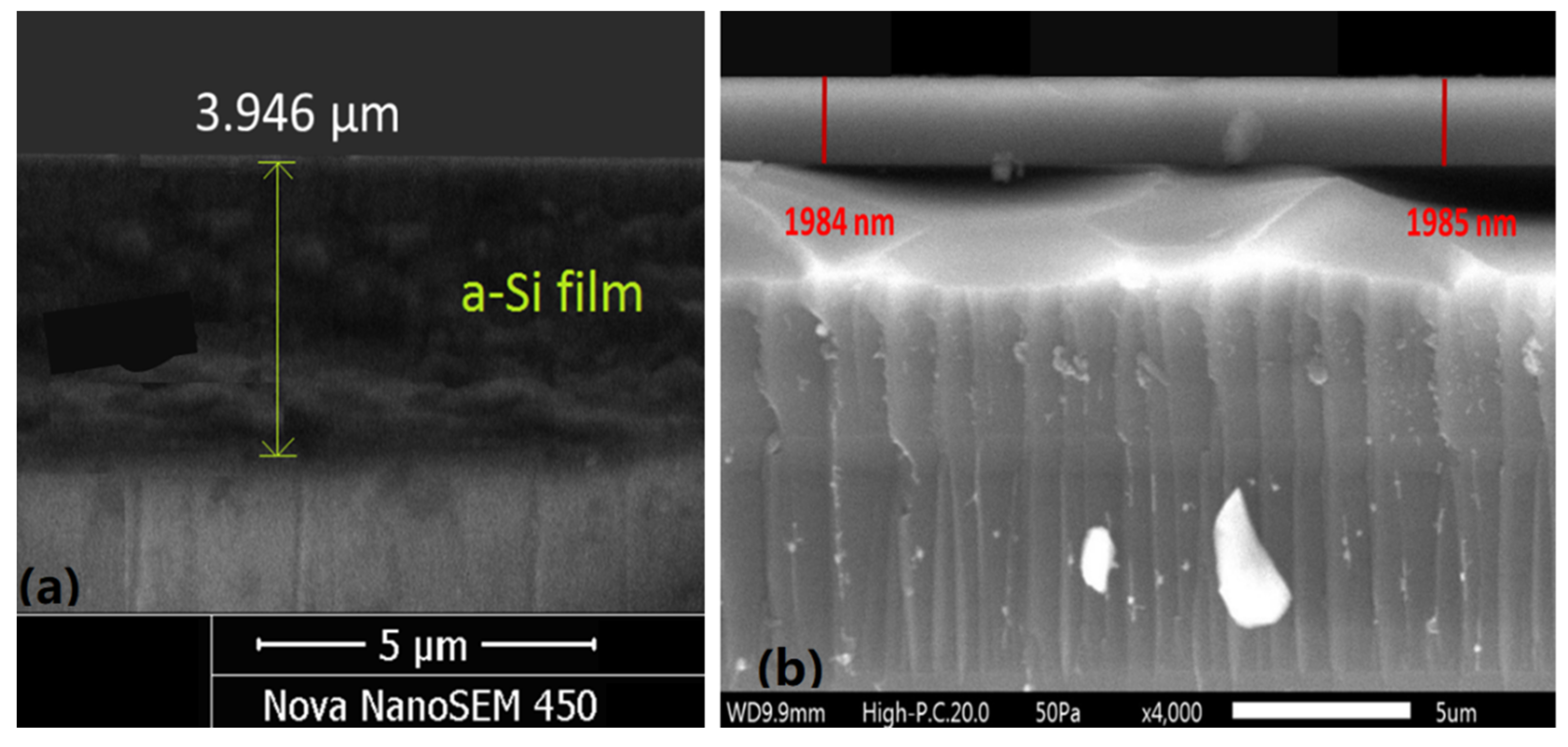
2.1. Preparation of the Specimens and Measuring the Transmittance Spectra T(λ)

The a-Si film has been deposited on 3.28-mm-thick Borofloat33 glass substrate by RF magnetron sputtering using RF power of 525 W, Ar gas with pressure of 0.13 Pa, and target-to-substrate distance of 6.1 cm, as described in [45]. The transmittance spectrum T(λ) of this specimen has been measured using a Perkin-Elmer Lambda 1050 UV/VIS/NIR spectrophotometer, with slit-width set at 2 nm, data collection interval of 1 nm, normal light incidence to the film, and illuminated area of 10 mm × 3 mm [50].
The As98Te2 film has been prepared by plasma-enhanced chemical vapor deposition for fifteen minutes on 1-mm-thick standard microscope slide glass substrate of Levenhuk, as described in [51]. T(λ) of this specimen has been measured using a Cary 5000 double-beam spectrophotometer of Agilent, with slit-width of 3.44 nm, data collection interval of 1 nm, normal light incidence to the film, and a circular illuminated area with 1 mm diameter [52].

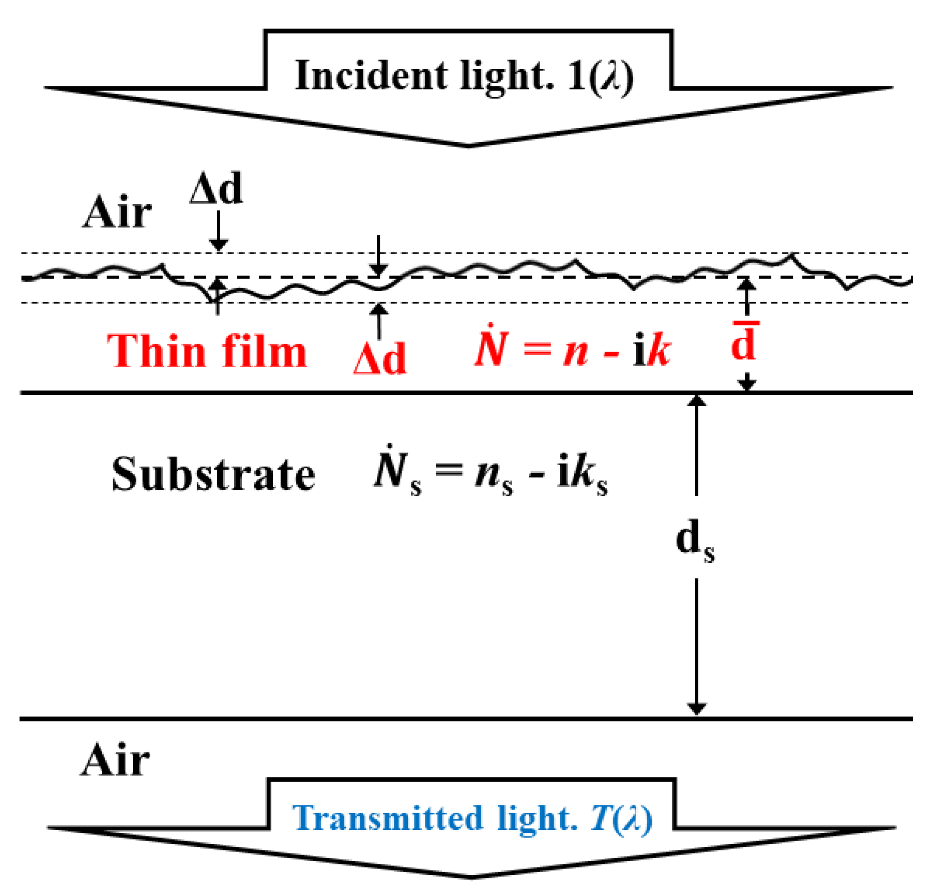
2.2. Details Regarding the Performed Accurate Thin Film Characterizations by EM for T(λ)

For both studied specimens, the refractive index of the substrate ns(λ) and its extinction coefficient ks(λ) are calculated by solving the system of two well-known equations for the transmittance Ts(λ) and the reflectance Rs(λ) of the bare substrate, which have also been measured [43,47].
It is pointed out that the thin-film characterizations reported in this study are founded on the EM for T(λ) from [43,45], as the dual transformation for computing T+(λ) and T(λ) is adopted from [47]. Regarding the proposed selection of an interval = [ 1,  2], over which the first stage of the characterization is performed most accurately, it is realized by including a program cycle increasing the integer  1e (representing  1), starting from  1e = 1. Moreover, one of the three optimized parameters determined by the EM for T(λ) from [43] is the number of the tangency wavelengths λt(), participating in the first stage of the characterization, denoted as  0 in Equation (4). Based on the above and Equation (4), the error metric employed for computing d ¯ , ∆d and m1[max(λt)] at the end of the first stage of the characterization is as follows:
δ d / d ¯ ( 1 e ) = ( 1 / d ¯ e ) = 1 e 2 e { d ¯ e d ¯ c e [ λ t ( ) ] } 2 2 e 1 e + 1 0
where  2e is automatically computed by the EM for T(λ) from [33]. Correspondingly,  1 =  1e for which δd/ d ¯ ( 1e) has a minimum value and  2 is its respective  2e, which completes the selection of the interval = [ 1, 2].
Besides the accurate computation of n(λ) and k(λ) in the second stage of the characterization, their approximations can also be computed there by solving the system of two equations for T+(λ) and T(λ), the computed result being denoted as (n, k) = f(T+, T).

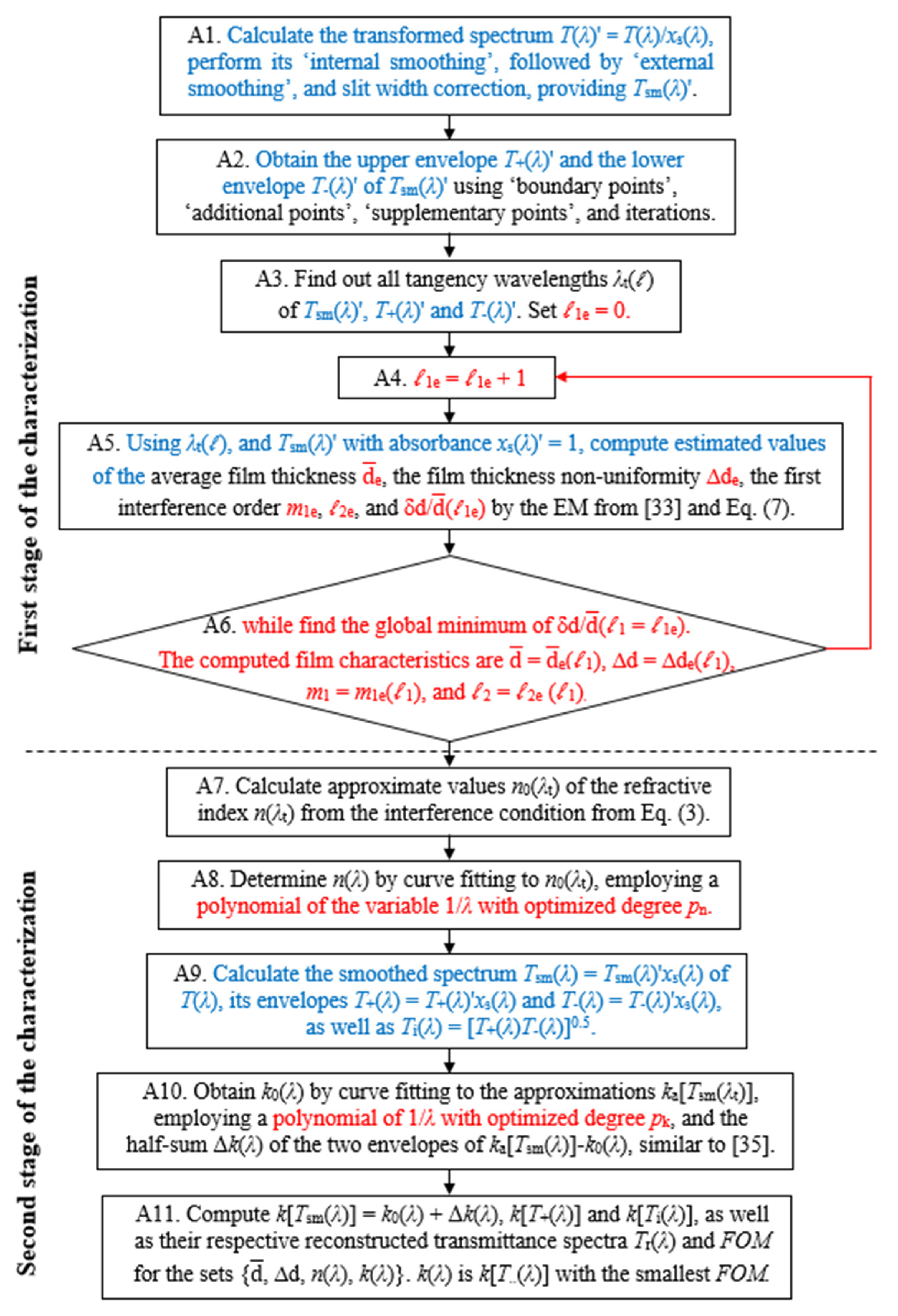
2.3. Algorithm for Accurate Thin-Film Characterization by EM for T(λ) Accounting for the Three Investigated Issues

An algorithm for accurate thin-film characterization accounting for the three investigated issues is developed, shown in Figure 2, and used in this study.
The above algorithm is founded on the algorithm of EM for T(λ) presented in [45], as the dual transformation for computing T+(λ) and T(λ) is adopted from [47], and the second and third investigated issues represent novelties. In principle, the algorithm from Figure 2 optimizes and utilizes the three parameters 1, 2 and Δd, which provide best fit of the spectrum Tsm(λ) (calculated from Equation (1)) to the experimental spectrum T(λ) in the interval [λt( 1), λt( 2)] from the spectral region of quasi-transparency and weak absorption of the film. To avoid using a local minimum of the error metric δd/ d ¯ at step A6 of the algorithm (instead of the needed global minimum), the optimization of the above three parameters is achieved by a ‘direct search′ [53] employing all plausible values of these parameters. Notably, Tsm(λ)’, featured at step A1, is obtained by external smoothing, similar to [45,47], which is beneficial for comparison of computed results from this paper with similar results from [45,47].
Furthermore, the estimated value d ¯ e( 1e) of the average film thickness (over the illuminated area) is calculated at step A5 by averaging the film thicknesses estimated for consecutive tangency wavelengths λt, as described in [43]. Correspondingly, δd (formulated by Equation (7)), obtained at step A6, represents the absolute error in the computation of the average film thickness d ¯ . Respectively, the global minimum of δd/ d ¯ ( 1e) (defined by Equation (7)), also computed at step A6, represents the relative error in the computation of the average film thickness d ¯ . Moreover, since the refractive index n(λ) of the film is computed based on Equation (3), its left side being the product 2n(λt) d ¯ and its right side being fixed for a given λt, the global minimum of δd/ d ¯ ( 1e) also represents the relative error in the computation of n(λ).
With respect to the above paragraph, characterization of four types of model thin film on glass substrate samples was performed in [54], by the EM for T(λ) from [33] using the error metric δd/ d ¯ ( 1e = 1). These four types of model films represent the four possible combinations of quasi-uniform or non-uniform dielectric or semiconductor film with or without a wide spectral region of quasi-transparency. The results from [54] have shown that this kind of characterization of such films should provide relative error │ d ¯ d ¯ M│/   d ¯ M < 0.1% in the computation of the average film thickness (where d ¯ M is the known average film thickness of the model film), as well as δd/ d ¯ M ≈ δd/ d ¯ < 0.1%. However, this kind of characterization of the films studied here has led to minimum values of δd/ d ¯ = 0.245% for the a-Si film, and δd/ d ¯ = 0.133% for the a-As98Te2 film, as reported in [47], thus missing the above target of δd/ d ¯ < 0.1%. Nevertheless, the above discussed data from [54] indicate that δd/ d ¯ (computed by the algorithm from Figure 2) represents the relative error │ d ¯ d ¯ true│/   d ¯ true (where d ¯ true is the true value of the average film thickness over the illuminated area) in the computation of the average film thickness, independent from the optical characteristics of the film.

2.4. Determination of Model Based Thin-Film Parameters Using Data from EM Characterization

A study of various amorphous semiconductors and glasses has shown that the dispersion of the refractive index n(λ) can be described by the Wemple-DiDomenico single-effective-oscillator model represented by the dependence, as follows:
n ( E )     1 + E 0 E d [ E 0 2 E 2 ( λ ) ]
where E(eV) = 1239.8/λ (nm) is the photon energy, E0 > E is the oscillator energy and Ed is the oscillator strength [55]. On the other hand, a-Si and a-As are amorphous semiconductors, and in many cases binary arsenic chalcogenide films are also amorphous semiconductors [56,57]. Taking into account the above, in this paper is used Wemple-DiDomenico plot of {n(E(λt))2 − 1}−1 versus E(λt)2, which should be represented by a straight line corresponding to Equation (8), for the studied a-Si and a-As98Te2 thin films. Since the accuracy of Equation (8) might decrease with increasing k(λ), the parameters E0 and Ed are determined by a low-energy linear regression to the Wemple-DiDomenico plot, and the static refractive index of the film is expressed from Equation (8) as follows:
n 0 = n ( E = 0 ) = n ( 0 ) = 1 + E d / E 0 .
Optical characteristics of other magnetron-sputtered a-Si thin films were studied in [50], depending on the pressure of the Ar gas, as the other technological parameters were identical to those for the a-Si thin film studied in this paper. The following empirical formula was obtained there:
E g     ( 8.3 n 0 ) / 3.8 ( e V )
where Eg is the band gap of magnetron-sputtered a-Si thin film. Equation (10) can be used for estimation of the band gap of the studied a-Si thin film.
It is also known that for amorphous semiconductors the following Tauc equation is usually valid:
( α E ) 1 / 2 B T ( E     E g )
for α(E) > 104 cm−1, where α(λ) = 4πk(λ)/λ is the absorption coefficient of the film, and BT is the Tauc slope [58]. Correspondingly, the band gap Eg can also be approximated employing Tauc plot of (αE)1/2 versus E and its high-energy linear regression with α(E) > 104 cm−1, as Eg represents the photon energy at which the regression line crosses the horizontal axis [58]. In order to use Tauc plot, n(E) is usually calculated from Equation (8), by substituting E0 and Ed determined from the Wemple-DiDomenico plot (assuming validity of the single-effective-oscillator model), followed by computation of α(λ) from Equation (1).
Besides, disorder in the local structure of material leads to presence of localized electronic states in its band gap, as it is generally accepted that α(E) of amorphous materials tails off exponentially, in the following:
α(E) = α0exp(E/EU)
in the interval α(E) [103, 104] cm−1, where EU is the Urbach energy and α0 is a pre-exponential factor [59,60]. Therefore, both EU and α0 can be derived using Urbach energy plot of log10[α(cm−1)] versus E and its linear regression in the interval log10[α(cm−1)] [3, 4]. Moreover, the photon energy corresponding to α(E) = 103 cm−1 is denoted by E03, and the photon energy corresponding to α(E) = 104 cm−1 is denoted by E04.
Furthermore, voids can occur in a-Si [61], and the voids volume fraction (compared to the entire volume of the material) has been approximated as follows:
f v o i d     [ 1 +   2 n 2 ( 0 ) ] [ n d e n s e 2 ( 0 ) n 2 ( 0 ) ] 3 n 2 ( 0 ) [ n d e n s e 2 ( 0 ) 1 ]
where ndense(0) is the static refractive index of a-Si without voids [50,62]. Besides, E0 = 2.873 eV and Ed = 36.404 eV have been reported for pure a-Si [63], and replacing these data in Equation (9) provides ndense(0) = 3.70. This result and Equation (13) permit calculation of the voids volume fraction for the studied a-Si thin film.

3. Results

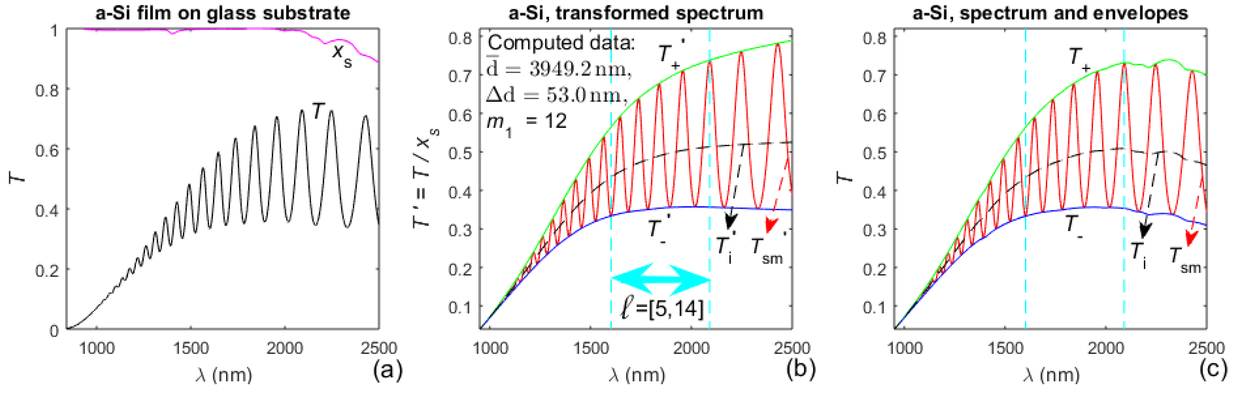
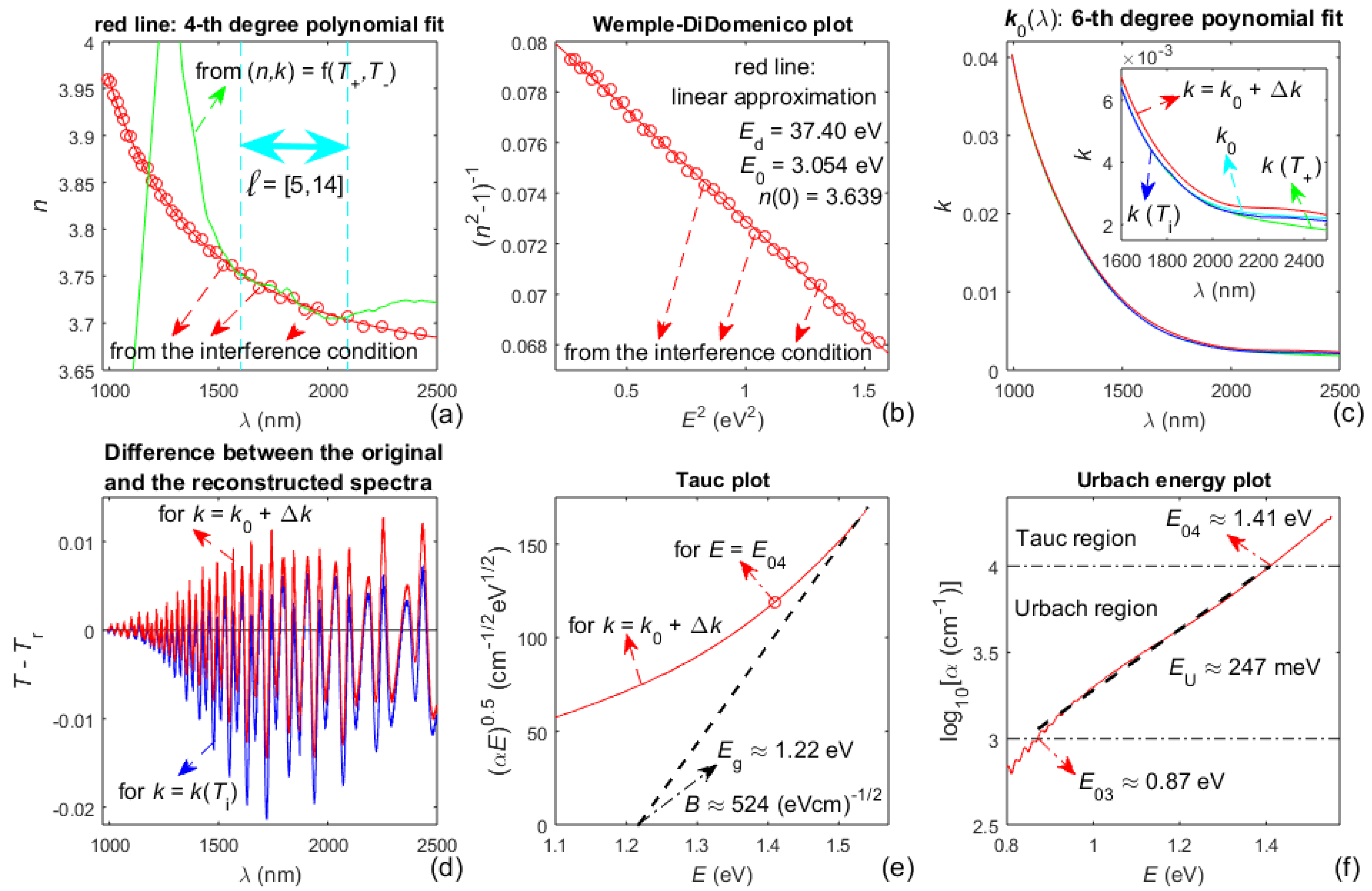
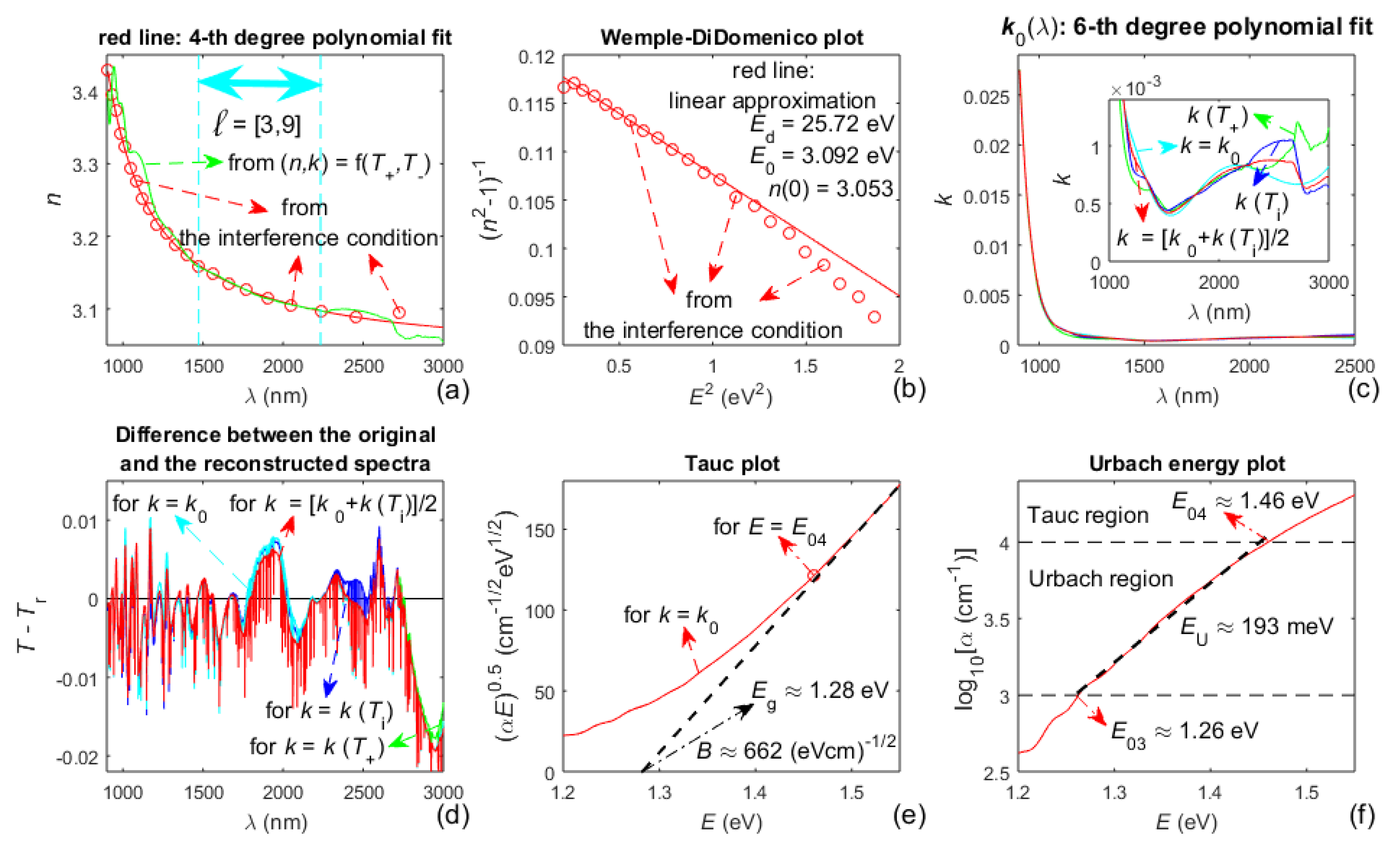
3.1. Characterization of the a-Si Film

Illustrations about the first stage from the characterization of the a-Si film, by the algorithm from Figure 2, are presented in Figure 3.
The variation in the interval  e = [ 1e,  2e] and its respective error metric δd/ d ¯ ( 1e) for the successively increasing  1e (in the process of selecting the interval = [ 1,  2], providing most accurate first step characterization), are shown in Table 1 for the a-Si film.
Pictures concerning the rest of the characterization of the a-Si film, based on the algorithm from Figure 2, are displayed in Figure 4.
FOM, computed from Equation (6) at step A11 from the algorithm, is presented in Table 2, for several choices of the extinction coefficient k(λ) of the a-Si film.

3.2. Characterization of the a-As98Te2 Film

Illustrations about the first stage from the characterization of the a-As98Te2 film, by the algorithm from Figure 2, are presented in Figure 5.
The variation in the interval  e = [ 1e,  2e] and its respective error metric δd/ d ¯ ( 1e), for the successively increasing  1e (in the process of selecting the interval = [ 1,  2], providing most accurate first step characterization), are shown in Table 3 for the a-As98Te2 film.
Pictures representing the rest of the characterization of the a-As98Te2 film, based on the algorithm from Figure 2, are displayed in Figure 6. FOM, computed from Equation (6) at step A11 from the algorithm, is presented in Table 4, for several choices of the extinction coefficient k(λ) of the a-As98Te2 film.
SEM images of cross-sections of both studied films are shown in Figure 7.

4. Discussion

With respect to the presented dual transformation, it is observed from Figure 3b,c and Figure 5b,c that the forward transformation provides T+(λ)′ and T(λ)′ without any kinks, unlike the envelopes T+(λ) and T(λ) reproducing the kinks in xs(λ). This indicates that such dual transformation should furnish more accurate points T+(λt) and T(λt) (needed for the first-stage characterization of the film), than using envelopes as the transparent substrate and correcting them only at λt with distinct xs(λt) < 1, as in [45]. Indeed, according to the data from Table 1 about the a-Si film, the error metric δd/ d ¯ ( 1e = 1) = 0.143% obtained in this study is significantly smaller than δd/ d ¯ ( 1e = 1) = 0.245% from [45], which confirms the above presumption. Moreover, employing the dual transformation is significantly simpler than using envelopes as the transparent substrate and correcting them only at λt with distinct xs(λt) < 1.
Regarding the selection of the interval = [ 1, 2], over which the first-stage characterization is most accurate (i.e., the interval corresponding to the smallest δd/ d ¯ ( 1e), = [5,14] for the a-Si film and = [3,9] for the As98Te2 film, as observed from Table 1 and Table 3. Besides, a review of Figure 3a,b and Figure 5a,b shows that the selected interval spreads out over a spectral region with xs(λ) 1, i.e., over a region where the substrate is quasi-transparent, for either of the studied films. This can be attributed to light scattering in the substrate, associated with the light absorption in the substrate, for wavelengths corresponding to xs(λ) < 1 [64]. Indeed, since light scattering in the substrate is not accounted for in the EM formulae, Equations (1) and (2) can predict somewhat larger values of the transmittance spectrum than the experimentally measured T(λ) in the region of distinct xs(λ) < 1. To mitigate this effect, the EM for T(λ) computes a visibly smaller extinction coefficient k(λ) of the film in the region of the smallest xs(λ) < 1; notably, such result is observed in the longest wavelength parts of Figure 4c, and especially of Figure 6c (since xs(λ) ≪ 1 for λ > 2700 nm). The above arguments indicate that the selection and employment of an interval = [ 1,  2], over which the first-stage characterization is most accurate, is especially beneficial for the characterization of a film on a non-transparent substrate. However, since the envelopes T+(λ) and T(λ) are less accurate in the long wavelength part of T(λ), e.g., due to luck of their precise boundary points there, use of such interval = [ 1,  2] is expected to also be favorable for the characterization of a thin film on a transparent substrate.
Based on the above, the employment of both the dual transformation (for non-transparent substrate) and the selected interval = [ 1,  2], corresponding to the smallest δd/ d ¯ ( 1e), should provide the most accurate thickness characteristics d ¯ and ∆d of the film.
However, the refractive index from (n,k) = f(T+, T), computed by solving the equations for T+(λ) and T(λ), is apparently inaccurate (compared to n(λ), obtained based on the interference condition), as observed from Figure 4a and Figure 6a. This is mainly due to the imperfection of the envelopes of T(λ), and indicates that n(λ) and k(λ) should not be computed only from Equation (2).
The concept of using a regression of n(λ) and k0(λ), by a polynomial of the optimized degree of 1/λ, has two advantages. First, it is consistent with the fact that the vast majority of dielectrics and semiconductors exhibit normal dispersion in the employed UV/VIS/NIR spectral region [19,21], as well as with its representation by the Cauchy’s dispersion formula [48,49]. Second, it eliminates the inconvenience of choosing a regression between a polynomial of the optimized degree of λ and a two-term exponential of λ, as in [45].
The Wemple-DiDomenico plot from Figure 4b illustrates that the dispersion of the refractive index n(λ) of the a-Si film is represented well by the single-effective-oscillator model and Equation (8). Besides, the static refractive index n0 = 3.639 of the a-Si film (sputtered using Ar gas with a pressure of 0.13 Pa), calculated from Equation (9), matches n0 ≈ 3.60 for similar films from [50]; inasmuch as n0 = 3.639 is quite close to ndense(0) = 3.70 for pure a-Si [63]. Moreover, replacing these values of n0 and ndense(0) in Equation (13) provides a voids volume fraction f v o i d     0 . The above facts indicate that the a-Si film studied here is quite dense and almost without voids.
The band gap Eg of the a-Si film is estimated by substituting n0 = 3.639 in Equation (10), which leads to Eg ≈ 1.20 eV, and Eg ≈ 1.22 eV is obtained by the Tauc plot from Figure 4e; whereas these data match Eg ≈ 1.23 eV for similar films from [50]. Furthermore, the Urbach energy EU ≈ 247 meV, derived based on the Urbach energy plot from Figure 4f, is similar to EU ≈ 266 meV for the respective films from [50]. Notably, it is observed from Table 2 that the minimum FOM achieved in this study is smaller than its respective value (for the same film and k = k0 + Δk) from [45], which implies that the characterization of the a-Si film presented here is more accurate than that from [45].
Concerning the second stage from the characterization of the a-As98Te2 film, the Wemple-DiDomenico plot from Figure 6b shows that the single-effective-oscillator model does not represent n(λ) well over all the tangency wavelengths λt of T(λ). Correspondingly, in the Tauc plot from Figure 6e, n(E) is used, calculated by a linear approximation of the higher photon energy region from the Wemple-DiDomenico plot. Regarding Table 4, since relatively smaller FOM are obtained in this study, for k = k0 and k(Ti), as well as that these two quantities are derived independently, the FOM is also computed for k = [k0 + k(Ti)]/2. Besides, it is observed from Table 4 that the minimum FOM achieved in this study is smaller than its respective value (for the same film) from [50], which indicates that the characterization of the a-Si film presented here is more accurate than that from [50].
Besides, the data in red color from Table 1 and Table 3, and the comments from the last two paragraphs of Section 2.3, indicate that δd/ d ¯ < 0.1% for either of the studied films. Furthermore, a comparison of the average film thickness from the SEM images with the computed d ¯ (shown in Figure 3b and Figure 5b), confirms that the relative error in the computation of the average film thickness does not exceed 0.1%, for both films. Moreover, these results represent achieving a relative error of 0.1% in the computation of both the average film thickness and the refractive index n(λ) of the film, as predicted in [54] and discussed in the last two paragraphs of Section 2.3.
On the other hand, it is observed from Equation (1) that Tsm(λ) ~ τa,fτf,sτf,ax ~ (n2 + k2)x, as usually x ≈ 1 for λ > min(λt) (this can be calculated from the formula for x, e.g., by replacing the already known d ¯ and k(λ) for the films studied here). Respectively, T(λ) ~ n2 + k2 for λ > min(λt), where n(λ) >> k(λ) for λ > min(λt) (it can be observed by comparing the data for T(λ), n(λ), and k(λ), e.g., from Figure 3, Figure 4, Figure 5 and Figure 6). These two relationships indicate that the increased accuracy achieved in this paper, in the computation of n(λ), results in a significantly larger increase in the computation accuracy of the extinction coefficient k(λ) in the region λ > min(λt), for each of the studied films. This fact contributes to the obtained decreased values of FOM, respectively, by 10% for the a-Si film compared to the data from [45] (as observed from Table 2), and by 2.8% for the a-As98Te2 film compared to the data from [47] (see Table 4).

5. Conclusions

Three issues are investigated for further increasing the accuracy of the characterization of a thin dielectric or semiconductor film on a substrate from T(λ) of the specimen, based on the EM.
1.
Firstly, it is demonstrated that the dual transformation, based on the product T(λ)xs(λ), increases the accuracy of the envelopes T+(λ) and T(λ) that are used in the computation of the average film thickness d ¯   and the film thickness non-uniformity ∆d, when the substrate is non-transparent. In practice, this approach resolves the problem of computing accurate envelopes of the interference spectrum T(λ) of a thin film on a non-transparent substrate.
2.
Secondly, how to select an interval = [ 1,  2] (representing the used λt) over which the first stage of the characterization is performed most accurately, is shown. The increased accuracy of the computation of d ¯   and ∆d of the studied a-Si and a-As98Te2 films indicates that employing this novel concept can increase the accuracy of the characterization of every thin dielectric or semiconductor film on a substrate, based on the EM for T(λ).
3.
Thirdly, the regression of n(λ) and k0(λ), by a polynomial of the optimized degree of 1/λ, is consistent with the Cauchy’s dispersion formula for materials with normal dispersion. Moreover, using only such regression eliminates the inconvenience of attempting another regression function.
The above three issues can be considered as useful supplementation to optimizing our envelope method for T(λ) (OEM for T(λ)), for thin-film characterization from [43]. In this sense, the EM implemented here, based on the algorithm from Figure 2, represents OEM for T(λ), providing and using optimized values of the characterization parameters ∆d,  1 and  2.
The comments from the last two paragraphs of Section 4, and our literature surveys from [43,44,45,47], indicate that the OEM characterizations presented here, corresponding to the data in red from Table 1, Table 2, Table 3 and Table 4, are undoubtedly the most accurate published optical thin-film characterizations of relatively thick films, only from T(λ).
Precise computation of both envelopes of T(λ) is needed for accurate film characterization, based on the algorithm from Figure 2, which requires the presence of at least five discernible interference extrema in T(λ). On the other hand, the number of interference extrema in T(λ) decreases with decreasing the average film thickness d ¯ (in accordance with Equation (3)). Moreover, the extinction coefficient k(λ) of dielectric or semiconductor film usually rises significantly with decreasing λ in the UV spectral region, which commonly leads to x(λ) → 0, T(λ) → 0 (according to Equation (1)) and the absence of interference extrema of T(λ) in the UV spectral region, for such films. The last two factors limit the applicability of the discussed OEM for T(λ), employing the algorithm from Figure 2, to dielectric or semiconductor films with average film thickness of usually at least 300 nm.
However, the reflectance spectrum R(λ) of a thin dielectric or semiconductor film, on a light-transmitting substrate, usually contains several discernible interference extrema in the UV spectral region (where there are no such extrema in the respective T(λ) of the same specimen). Correspondingly, it is expected that the OEM for R(λ) should be applicable to dielectric and semiconductor films that are significantly thinner than 300 nm. Notably, our group is in the advanced stage of development of such OEM for R(λ).

Author Contributions

Conceptualization, D.M.; methodology, D.M. and E.M.; software, D.M. and G.G.; validation, D.M. and G.G.; formal analysis, D.M. and E.M.; investigation, D.M. and G.A.; resources, D.M., E.M., S.R. and E.S.; data curation, D.M. and G.G.; writing—original draft preparation, D.M. and E.M.; writing—review and editing, G.A.; visualization, D.M., and G.G.; supervision, D.M.; project administration, G.A., S.R. and E.S.; funding acquisition, G.A. All authors have read and agreed to the published version of the manuscript.

Funding

This work was supported by the European Regional Development Fund within the Operational Programme “Science and Education for Smart Growth 2014–2020” under the Project CoE “National Center of Mechatronics and Clean Technologies”, contract No. BG05M2OP001-1.001-0008, L10S7 SynChaLab. The As98Te2 film on substrate specimens have been prepared with funding from the Russian Science Foundation grant 16-12-00038.

Institutional Review Board Statement

Not applicable.

Informed Consent Statement

Not applicable.

Data Availability Statement

The data underlying this article will be shared on reasonable request from the corresponding author.

Acknowledgments

The authors express gratitude to Aleksey Nezhdanov from the Laboratory of Functional Nanomaterials, Lobachevsky University, Nizhny Novgorod, Russia for providing data for the a-As98Te2 thin film on glass substrate specimen.

Conflicts of Interest

The authors declare no conflict of interest. The funders had no role in the design of the study; in the collection, analyses, or interpretation of data; in the writing of the manuscript, or in the decision to publish the results.

References

  1. Poortmans, J.; Arkhipov, V. Thin Film Solar Cells: Fabrication, Characterization and Applications, 1st ed.; Wiley: Hoboken, NJ, USA, 2009; pp. 41–55. [Google Scholar]
  2. Stenzel, O. Optical Coatings: Material Aspects in Theory and Practice, 1st ed.; Springer: Heidelberg, Germany, 2016; pp. 35–51. [Google Scholar]
  3. The Role of Thin Film in Optical Field. Available online: https://www.alcatechnology.com/en/blog/the-role-of-thin-film-in-optical-field/ (accessed on 16 June 2021).
  4. Tamang, A.; Hongsingthong, A.; Sichanugrist, P.; Jovanov, V.; Gebrewold, H.T. On the potential of light trapping in multiscale textured thin film solar cells. Sol. Energy Mater. Sol. Cells 2016, 144, 300–308. [Google Scholar] [CrossRef]
  5. Islam, K.; Chowthury, F.; Alnuaimi, A.; Nayfeh, A. ~10% increase in short-current density using 100nm plasmonic Au nanoparticles on thin film n-i-p a-Si:H solar cells. In Proceedings of the IEEE Conference on Photovoltaic Specialists (PVSC 40), Denver, CO, USA, 1–13 June 2014; pp. 3071–3075. [Google Scholar]
  6. Diallo, A.K.; Ly, A.H.B.; Ndiaye, D.; Kobor, D.; Pasquinelli, M.; Diallo, A.K. Influence of temperature and pentacene thickness on the electrical parameters in top gate organic thin film transistor. AMPC 2017, 7, 85–98. [Google Scholar] [CrossRef] [Green Version]
  7. Jhu, J.C.; Chang, T.C.; Chang, K.C.; Yang, C.Y.; Chou, W.C.; Chou, C.H.; Chung, W.C. Investigation of hydration reaction-induced protons transport in etching-stop a-InGaZnO thin-film transistors. IEEE Electron. Device Lett. 2015, 36, 1050–1052. [Google Scholar] [CrossRef]
  8. Ta’eed, V.G.; Baker, N.J.; Fu, L.; Finsterbusch, K.; Lamont, M.R.E.; Moss, D.J.; Nguyen, H.C.; Eggleton, B.J.; Choi, D.Y.; Madden, S.; et al. Ultrafast all-optical chalcogenide glass photonic circuits. Opt. Express 2007, 15, 9205–9221. [Google Scholar] [CrossRef]
  9. Song, S.; Carlie, N.; Boudies, J.; Petit, L.; Richardson, K.; Arnold, C.B. Spin coating of Ge23Sb7S70 chalcogenide glass thin films. J. Non-Cryst. Solids 2009, 355, 2272–2278. [Google Scholar] [CrossRef]
  10. Waldman, D.A.; Li, H.Y.S.; Cetin, E.A. Holographic recording properties in thick films of ULSH-500 photopolymer. In Proceedings of the Diffractive and Holographic Device Technologies and Applications V (Proc. SPIE 3291), San Jose, CA, USA, 28–29 January 1998; pp. 89–98. [Google Scholar]
  11. Navarro-Fuster, V.; Ortuno, M.; Gallego, S.; Márquez, A.; Beléndez, A.; Pascual, I. Biophotopol’s energetic sensitivity improved in 300 μm layer by tuning the recording wavelength. Opt. Mater. 2016, 52, 111–115. [Google Scholar] [CrossRef] [Green Version]
  12. Dudney, N.J.; Jang, Y.I. Analysis of thin-film lithium batteries with cathodes of 50 nm to 4 μm thick LiCoO2. J. Power Sources 2003, 119, 300–304. [Google Scholar] [CrossRef]
  13. Huang, X.D.; Zhang, F.; Gana, X.F.; Huanga, Q.A.; Yang, J.Z.; Laic, P.T.; Tang, W.M. Electrochemical characteristics of amorphous silicon carbide film as a lithium-ion battery anode. RSC Adv. 2018, 8, 5189–5196. [Google Scholar] [CrossRef] [Green Version]
  14. Soriaga, M.P.; Stickney, J.; Bottomley, L.A.; Kim, Y.G. Thin Films: Preparation, Characterization, Applications, 1st ed.; Springer: Boston, MA, USA, 2002; pp. 37–45. [Google Scholar]
  15. Hilfiker, J.N.; Singh, N.; Tiwald, T.; Convey, D.; Smith, S.M.; Bakerb, J.H.; Tompkins, H.G. Survey of methods to characterize thin absorbing films with Spectroscopic Ellipsometry. Thin Solid Film. 2008, 516, 7979–7989. [Google Scholar] [CrossRef]
  16. Poelman, D.; Smet, P.J. Methods for the determination of the optical constants of thin films from single transmission measurements: A critical review. J. Phys. D 2003, 36, 1850–1857. [Google Scholar] [CrossRef]
  17. Stenzel, O. The Physics of Thin Film Optical Spectra, 1st ed.; Springer: Heidelberg, Germany, 2016; pp. 79–81. [Google Scholar]
  18. Shaaban, E.R.; Afify, N.; El-Taher, A. Effect of film thickness on microstructure parameters and optical constants of CdTe thin films. J. Alloys Compd. 2009, 482, 400–404. [Google Scholar] [CrossRef]
  19. Kaflé, B.P. Chemical Analysis and Material Characterization by Spectrophotometry, 1st ed.; Kindle: Seattle, DC, USA, 2019; pp. 72–75. [Google Scholar]
  20. Tompkins, H.G.; Hilfiker, J.N. Spectroscopic Ellipsometry: Practical Application to Thin Film Characterization, 1st ed.; Momentum Press: New York, NY, USA, 2015; pp. 84–88. [Google Scholar]
  21. Stenzel, O.; Ohlídal, M. Optical Characterization of Thin Solid Films, 1st ed.; Springer: Heidelberg, Germany, 2016; pp. 93–99. [Google Scholar]
  22. Swanepoel, R. Determining refractive index and thickness of thin films from wavelength measurements only. J. Opt. Soc. Am. A 1985, 2, 1339–1343. [Google Scholar] [CrossRef]
  23. Gao, L.; Lemarchand, F.; Lequime, M. Refractive index determination of SiO2 layer in the UV/Vis/NIR range: Spectrophotometric reverse engineering on single and bi-layer designs. J. Europ. Opt. Soc. Rap. Public. 2013, 8, 1–8. [Google Scholar] [CrossRef] [Green Version]
  24. Frey, H.; Khan, H.R. Handbook of Thin Film Technology, 1st ed.; Springer: Berlin, Germany, 2015; pp. 24–41. [Google Scholar]
  25. Yen, S.T.; Chung, P.K. Extraction of optical constants from maxima of fringing reflectance spectra. Appl. Opt. 2015, 54, 663–668. [Google Scholar] [CrossRef]
  26. Ohlídal, I.; Vohánka, J.; Buršíková, V.; Franta, D.; Čermák, M. Spectroscopic ellipsometry of inhomogeneous thin films exhibiting thickness non-uniformity and transition layers. Opt. Express 2020, 28, 160–174. [Google Scholar] [CrossRef]
  27. Vohánka, J.; Franta, D.; Čermák, M.; Homola, V.; Buršíková, V.; Ohlídal, I. Ellipsometric characterization of highly non-uniform thin films with the shape of thickness non-uniformity modeled by polynomials. Opt. Express 2020, 28, 5492–5506. [Google Scholar] [CrossRef] [PubMed]
  28. Surface Roughness Parameters. Available online: https://www.keyence.eu/ss/products/microscope/roughness/line/tab02_a.jsp/ (accessed on 16 June 2021).
  29. Thin-Film Interference. Available online: https://en.wikipedia.org/wiki/Thin-film_interference/ (accessed on 16 June 2021).
  30. Thin-Film Interference. Available online: https://www.britannica.com/science/light/Thin-film-interference (accessed on 16 June 2021).
  31. Tompkins, H.; Irene, E.A. Handbook of Ellipsometry, 1st ed.; William Andrew Publishing: Norwich, CT, USA, 2006; pp. 102–143. [Google Scholar]
  32. Ogieglo, W.; Wormeester, H.; Eichhorn, K.J.; Wessling, M.; Benes, N.E. In situ ellipsometry studies on swelling of thin polymer films. Prog. Polym. Sci. 2015, 42, 42–78. [Google Scholar] [CrossRef]
  33. Mieghem, P.V. Theory of band tails in heavily doped semiconductors. Rev. Mod. Phys. 1992, 64, 755–793. [Google Scholar] [CrossRef]
  34. Fedyanin, D.Y.; Arsenin, A.V. Surface plasmon polariton amplification in metal-semiconductor structures. Opt. Express 2011, 19, 12524–12531. [Google Scholar] [CrossRef]
  35. Cisowski, J.; Jarzabek, B.; Jurusik, J.; Domanski, M. Direct determination of the refraction index normal dispersion for thin films of 3, 4, 9, 10-perylene tetracarboxylic dianhydride (PTCDA). Opt. Appl. 2012, 42, 181–192. [Google Scholar]
  36. Grassi, A.P.; Tremmel, A.J.; Koch, A.W.; El-Khozondar, H.J. On-line thickness measurement for two-layer systems on polymer electronic devices. Sensors 2013, 13, 15747–15757. [Google Scholar] [CrossRef] [Green Version]
  37. Brinza, M.; Emelianova, E.V.; Adriaenssens, G.Y. Nonexponential distributions of tail states in hydrogenated amorphous silicon. Phys. Rev. B 2005, 71, 115209. [Google Scholar] [CrossRef]
  38. Swanepoel, R. Determination of the thickness and optical constants of amorphous silicon. J. Phys. E 1983, 16, 1214–1222. [Google Scholar] [CrossRef]
  39. Google Scholar. Available online: https://scholar.google.com/scholar?cites=9869860102796010609&as_sdt=2005&sciodt=0,5&hl=bg (accessed on 1 August 2021).
  40. Minkov, D.A. DSc Thesis: Characterization of Thin Films and Surface Cracks by Electromagnetic Methods and Technologies; Technical University: Sofia, Bulgaria, 2018; pp. 114–119. [Google Scholar]
  41. Swanepoel, R. Determination of surface roughness and optical constants of inhomogeneous amorphous silicon films. J. Phys. E Sci. Instrum. 1984, 17, 896–903. [Google Scholar] [CrossRef]
  42. Leal, J.M.G.; Alcon, R.P.; Angel, J.A.; Minkov, D.A.; Marquez, E. Influence of substrate absorption on the optical and geometrical characterization of thin dielectric films. Appl. Opt. 2002, 41, 7300–7308. [Google Scholar] [CrossRef] [PubMed]
  43. Minkov, D.A.; Gavrilov, G.M.; Angelov, G.V.; Moreno, G.M.D.; Vazquez, C.G.; Ruano, S.M.F.; Marquez, E. Optimisation of the envelope method for characterisation of optical thin film on substrate specimens from their normal incidence transmittance spectrum. Thin Solid Film. 2018, 645, 370–378. [Google Scholar] [CrossRef]
  44. Minkov, D.A.; Angelov, G.V.; Nestorov, R.N.; Marquez, E.; Blanco, E.; Ruiz-Perez, J.J. Comparative study of the accuracy of characterization of thin films a-Si on glass substrates from their interference normal incidence transmittance spectrum by the Tauc-Lorentz-Urbach, the Cody-Lorentz-Urbach, the optimized envelopes and the optimized graphical methods. Mater. Res. Express 2019, 6, 036410. [Google Scholar]
  45. Minkov, D.A.; Angelov, G.V.; Nestorov, R.N.; Marquez, E. Perfecting the dispersion model free characterization of a thin film on a substrate specimen from its normal incidence interference transmittance spectrum. Thin Solid Film. 2020, 706, 137984. [Google Scholar] [CrossRef]
  46. Precision Cover Glasses and Microscope Slides. Available online: https://www.thorlabs.de/newgrouppage9.cfm?objectgroup_id=9704/ (accessed on 16 June 2021).
  47. Minkov, D.A.; Angelov, G.; Nestorov, R.; Nezhdanov, A.; Usanov, D.; Kudryashov, M.; Mashin, A. Optical characterization of AsxTe100-x Films Grown by Plasma Deposition Based on the Advanced Optimizing Envelope Method. Materials 2020, 13, 2981. [Google Scholar] [CrossRef] [PubMed]
  48. Cauchy and Related Empirical Dispersion Formulae for Transparent Materials, Technical Note. Spectroscopic Ellipsometry TN14. Available online: https://www.horiba.com/fileadmin/uploads/Scientific/Downloads/OpticalSchool_CN/TN/ellipsometer/Cauchy_and_related_empirical_dispersion_Formulae_for_Transparent_Materials.pdf (accessed on 6 June 2020).
  49. Smith, D.Y.; Inokuti, M.; Karstens, W.A. generalized Cauchy dispersion formula and the refractivity of elemental semiconductors. J. Phys. Condens. Matter. 2001, 13, 3883–3893. [Google Scholar] [CrossRef]
  50. Márquez, E.; Saugar, E.; Díaz, J.M.; Vázquez, C.G.; Ruano, S.M.F.; Blanco, E.; Ruiz-Pérez, J.J.; Minkov, D.A. The influence of Ar pressure on the structure and optical properties of non-hydrogenated a-Si thin films grown by rf magnetron sputtering onto room temperature glass substrates. J. Non-Cryst. Solids 2019, 517, 32–43. [Google Scholar] [CrossRef]
  51. Mochalov, L.; Nezhdanov, A.; Kudryashov, M.; Loghunov, A.; Strikovskiy, A.; Gushchin, M.; Chidichomo, G.; DeFilipo, G.A.; Mashin, A. Influence of plasma-enhanced chemical vapor deposition parameters on characteristics of As–Te chalcogenide films. Plasma Chem. Plasma Process. 2017, 37, 1417–1429. [Google Scholar] [CrossRef]
  52. Mochalov, L.; Dorosz, D.; Nezhdanov, A.; Kudryashov, M.; Zelentsov, S.; Usanov, D.; Logunov, A.; Mashin, A.; Gogova, D. Investigation of the composition-structure-property relationship of AsxTe100−x films prepared by plasma deposition. Spectrochim. Acta A Mol. Biomol. Spectrosc. 2018, 191, 211–216. [Google Scholar] [CrossRef]
  53. Bartz, A.E. Basic Statistical Concepts, 4th ed.; Prentice-Hall Inc.: Upper Saddle River, NJ, USA, 1999; pp. 43–47. [Google Scholar]
  54. Nestorov, R.N. Selection of error metric for accurate characterization of a thin dielectric or semiconductor film on glass substrate by the optimizing envelope method. Int. J. Adv. Res. Sci. Eng. Technol. 2020, 7, 1–11. [Google Scholar]
  55. Wemple, S.H. Refractive-index behavior of amorphous semiconductors and glasses. Phys. Rev. B 1973, 7, 3767–3777. [Google Scholar] [CrossRef]
  56. Amorphous Silicon. Available online: https://en.wikipedia.org/wiki/Amorphous_silicon/ (accessed on 18 June 2021).
  57. Tylor, P.C. Nuclear Quadrupole resonance in amorphous semiconductors. Z. Naturforsch. 1996, 51, 603–610. [Google Scholar] [CrossRef]
  58. Knief, S.; von Niessen, W. Disorder, defects, and optical absorption in a-Si and a-Si:H. Phys. Rev. B 1999, 59, 12940–12946. [Google Scholar] [CrossRef]
  59. Pan, Y.; Inam, F.; Zhang, M.; Drabold, D.A. Atomistic origin of Urbach tails in amorphous silicon. Phys. Rev. Lett. 2008, 100, 206403. [Google Scholar] [CrossRef] [Green Version]
  60. Zaynobidinov, S.; Ikramov, R.G.; Jalalov, R.M. Urbach energy and the tails of the density of states in amorphous semiconductors. J. Appl. Spectrosc. 2011, 78, 223–227. [Google Scholar] [CrossRef]
  61. Guerrero, E.; Strubbe, D.A. Computational generation of voids in a-Si and a-Si:H by cavitation at low density. Phys. Rev. Mater. 2020, 4, 025601. [Google Scholar] [CrossRef] [Green Version]
  62. Bruggeman, D.A.G. Berechnung verschiedener physikalischer konstanten von heterogenen substanzen i. dielektrizitätskonstanten und leitfähigkeiten der mischkörper aus isotropen substanzen. Ann. Phys. 1935, 416, 636–664. [Google Scholar] [CrossRef]
  63. Chen, H.; Shen, W.Z. Perspectives in the characteristics and applications of Tauc-Lorentz dielectric function model. Eur. Phys. J. B 2005, 43, 503–507. [Google Scholar] [CrossRef]
  64. Passive Optical Properties of Glass. Available online: https://www.lehigh.edu/imi/teched/GlassProp/Slides/GlassProp_Lecture16_Lucas.pdf (accessed on 25 June 2021).
Figure 1. Sketch of transmittance T(λ) of light through a sample consisting of a thin film on a substrate. The thin film and its main optical characteristics are represented in red. ∆d is half of the difference between the maximum value and the minimum value of the film thickness d over the illuminated area on the free surface of the film.
Materials 14 04681 g001
Figure 2. Algorithm for accurate thin-film characterization by EM for T(λ) accounting for the three investigated issues. The text in black corresponds to the algorithm from [45], the text in blue represents the dual transformation for computing the envelopes T+(λ) and T(λ) of Tsm(λ) from [47], as the text and arrow in red are related to the second and the third investigated issues.
Materials 14 04681 g002
Figure 3. Transmittance-related spectra and results from the first-stage characterization of the a-Si film: (a) transmittance spectrum T(λ) of the specimen, and substrate absorbance xs(λ); (b) forward transformed spectra and results from the first stage characterization. The selected interval = [5,14] providing the most accurate first-stage characterization is marked by double arrow; (c) the reverse-transformed smoothed spectrum Tsm(λ), its envelopes T+(λ) and T(λ), and Ti(λ) from Equation (5).
Materials 14 04681 g003
Figure 4. Illustrations regarding computed material characteristics of the a-Si film. (a) The refractive index n(λ) determined at steps A7 and A8 from the algorithm; (b) Wemple-DiDomenico plot; (c) data for the extinction coefficient k(λ) from steps A10 and A11; (d) differences T(λ)–Tr(λ), from step A11, for k = k(Ti) and k = k0 + Δk; (e) Tauc plot; (f) Urbach energy plot.
Materials 14 04681 g004
Figure 5. Transmittance-related spectra and results from the first-stage characterization of the a-As98Te2 film: (a) transmittance spectrum T(λ) of the specimen, and substrate absorbance xs(λ); (b) forward-transformed spectra and results from the first-stage characterization. The selected interval = [3,9] providing the most accurate first-stage characterization is marked by double arrow; (c) the reverse-transformed smoothed spectrum Tsm(λ), its envelopes T+(λ) and T(λ), and Ti(λ) from Equation (5).
Materials 14 04681 g005
Figure 6. Illustrations regarding computed material characteristics of the As98Te2 film. (a) The refractive index n(λ) determined at steps A7 and A8 from the algorithm; (b) Wemple-DiDomenico plot; (c) data for the extinction coefficient k(λ) from steps A10 and A11; (d) differences T(λ)–Tr(λ), from step A11, for k = k(Ti), k = k0, k = k(T+) and k = [k0 + k(Ti)]/2; (e) Tauc plot using n(E) calculated by a linear approximation of the higher-energy region from the Wemple-DiDomenico plot; (f) Urbach energy plot.
Materials 14 04681 g006
Figure 7. SEM images of cross-sections of the studied films. (a) for the a-Si film and (b) for the As98Te2 film.
Materials 14 04681 g007
Table 1. The interval  e = [ 1e,  2e] and δd/ d ¯ ( 1e), for successively increasing 1e, from the first-stage characterization of the a-Si film. The data about δd/ d ¯ ( 1e=1) (%) from this study are in blue color, and in green—from [45]; whereas the minimum value of δd/ d ¯ ( 1e) (%) is in red.
a-Si, First-Stage Characterizationfrom Ref. [45]
e = [ 1e, 2e][1,18][2,18][3,26][4,26][5,14][6,26][1,16]
δ d / d ¯ ( 1e) (%)0.1430.1460.1650.1680.09010.1700.245
computed film characteristicsfor = [5,14] :   d ¯ = 3949.2 nm, Δd = 53.0 nm, m1 = 12 d ¯ = 3929.9 nm, Δd = 53.5 nm, m1 = 12
Table 2. The figure of merit FOM for different options about the extinction coefficient k(λ) of the a-Si film. The minimum of FOM achieved in this study is in red color, and the minimum of FOM from [45] is in green.
a-Si, Second-Stage Characterizations
FOMfor k = k0for k = k0 + Δkfor k(T+)for k(Ti)for [k0 + Δk + k(Ti)]/2
From ref. [45]7.36 × 10−35.71 × 10−37.78 × 10⁻³--
this study6.65 × 10−35.19 × 10−37.41 × 10−36.91 × 10−35.80 × 10−3
Table 3. The interval  e = [ 1e,  2e] and δd/ d ¯ ( 1e), for successively increasing 1e, from the first-stage characterization of the a-As98Te2 film. The minimum of δd/ d ¯ ( 1e) (%) from this study is in red color, and the minimum of δd/ d ¯ ( 1e) (%) from [47] is in green.
a-As98Te2, First-Stage CharacterizationFrom Ref. [47]
e = [ 1e, 2e][1,19][2,9][3,9][4,9][5,9][6,9][2,12]
δ d / d ¯ ( 1e) (%)0.3080.08570.04260.04550.04910.04970.133
computed film characteristicsfor = [3,9]: d ¯ = 1983.2 nm, Δd = 23.9 nm, m1 = 4.5 d ¯ = 1983.8 nm, Δd = 22.7 nm, m1 = 4.5
Table 4. The figure of merit FOM for different options about the extinction coefficient k(λ) of the a-As98Te2 film. The minimum of FOM achieved in this study is in red color, and the minimum of FOM from [47] is in green.
a-As98Te2, Second-Stage Characterizations
FOMfor k = k0for k = k0 + Δkfor k(T+)for k(Ti)for [k0 + k(Ti)]/2
from [47]4.36 × 10−34.26 × 10−33.96 × 10−33.74 × 10−3-
this study3.89 × 10−33.89 × 10−34.38 × 10−33.87 × 10−33.64 × 10−3
Publisher’s Note: MDPI stays neutral with regard to jurisdictional claims in published maps and institutional affiliations.

