Abstract
With classical molecular dynamics simulations, we demonstrated that doping of the InP crystal with Zn and S atoms reduces the pressure of the phase transformation as well as inhibits the development of a dislocation structure. On this basis, we propose a method for determining the phenomenon that initiates nanoscale plasticity in semiconductors. When applied to the outcomes of nanoindentation experiments, it predicts the dislocation origin of the elastic-plastic transition in InP crystal and the phase transformation origin of GaAs incipient plasticity.
1. Introduction
Recently, Wong et al. [] used nanoindentation to create a stable, metallic nanoparticle at the surface of Si crystal. This nanostructure can be thought of as an efficient light-catching system with promising applications in photovoltaic technology [,]. Unexpectedly, the authors breathed new life into the importance of research of phenomena that can initiate nanoscale plasticity in semiconductor crystals. Indeed, it is not possible to create metallic nanoislands by means of nanoindentation in all semiconductors, but rather only in those whose plastic deformation is initiated by the transformation to the high-pressure metallic phase.
On the whole, elastic-plastic transition in dislocation-free semiconductor nanovolume is a controversial issue, as it involves both the phase transformations and dislocation generation. For example, nanoindentation-induced plasticity of Si crystal can be initiated by phase transformation or nucleation of dislocations, depending on experimental conditions [,,]. Interestingly, the results of nanoindentations accompanied by Raman spectroscopy [,,] indicate a complex course of phase transformations in silicon: formation of Si-II (-tin) phase during loading and Si-III (bc8) and Si-XII (r8) phases during unloading. Regarding other semiconductors, it is worth noting that the elastic-plastic transition in GaAs crystal is initiated by the phase transformation [,,], while nanoscale plasticity in GaN is exclusively governed by the activity of dislocations [,].
Determination of the phenomenon which initiates nanoindentation-induced elastic-plastic transition seems to be a difficult task due to the fact that crystal deformation occurs in very small volumes. One of the methods that can be used involves disturbing the structure of a semiconductor by introducing dopant atoms and then examining how the doping affects the contact pressure during the elastic-plastic transition. To be more precise, we will focus on theoretical demonstration and experimental verification of how doping influences the elastic-plastic transition in one of the most important semiconductors in technology, namely InP. A review of the scientific literature shows that the optoelectronic properties of InP are basically known, while the cause of its elastic-plastic transition has not yet been fully determined. Looking at the available data, the dominant role of dislocation activity becomes clear in the plastic deformation of InP [,,,,,,,], without the participation of structural phase transformations []. However, the results of mentioned structural investigations were carried out after nanoindentation experiments, so it is premature to exclude the effect of phase transformation on the incipient plasticity of InP.
In this letter, classical molecular dynamic (MD) simulations were used to demonstrate the effect of Zn- as well as S-doping on both the transformation from B3 (zincblende) to B1 (rocksalt) crystal structure of InP and dislocation generation during nanoindentation of the InP surface. The results of MD simulations allowed us to propose a method to distinguish the origin of the incipient plasticity of semiconductors.
2. Materials and Methods
Molecular dynamics simulations were performed with the LAMMPS software []. In order to study the effect of Zn- and S-doping on the pressure of phase transformation in InP crystal, the system (supercell) composed of B3 unit cells (lattice constant Å []) was used. Doping with Zn and S atoms was chosen because it is technologically important giving p-type and n-type electrical conductivity, respectively. Moreover, the dopant atoms build into the InP crystal lattice and create relatively simple substitutional point defects: , []. In our simulations, the defect was defined by the replacement of one X atom of the supercell by atom Y, which resulted in reasonable concentration of dopants. Interatomic interactions in pure InP crystal were described by the Vashishta potential [,], while interactions with Zn and S atoms were modeled by the Lennard-Jones potential (refer to Supplementary Materials). The Velocity-Verlet time integration algorithm, with an increment of , was used through the simulations, while the canonical (NVT) ensemble was employed to control the thermodynamical variables. Prior to running deformation simulations, the system was relaxed to a thermal equilibrium at the target temperature of . The volume of the supercell was then reduced by varying the length of its edges up to 10% in 100,000 time steps. Structural changes, recorded every 500 time steps, were analyzed using the OVITO software [].
Nanoindentations of the B3 phase of InP were simulated at . A block of InP crystal (, 1,930,600 atoms) was indented by a rigid sphere () in the surface. The interactions between the diamond indenter tip and InP crystal were modeled by the repulsive term of the Buckingham potential with 4 Å cut-off radius. Nanodeformation was accomplished in a quasi-static manner by a sequence of indenter’s displacements with an increment of Å every .
Examples of Lammps scripts implementing the above simulations can be found in Supplementary Materials.
3. Results and Discussion
To investigate the effect of doping on the pressure of the phase transformation in InP, a supercell consisting of unit cells ( Å) was used. As the initial edge length Å of the supercell gradually decreases (compression), the B3 phase of undoped InP becomes unstable at Å when the pressure p approaches the value (Figure 1). A further decrease in L reduces the pressure to the level of ∼4 , indicating formation of some high-pressure phase. The atomic configuration presented in Figure 2a ( Å, ) exhibits details characteristic for the B1 lattice. Indeed, the group of atoms shown in Figure 2a, cut from the column surrounded by the green dashed line, undoubtedly forms the B1 unit cell (see also Figure S1 in Supplementary Materials). In order to estimate the lattice constant of the B1 phase, we used the method based on the radial distribution function (RDF). Figure 2b shows RDFs calculated for the nearest In atoms in B3 ( Å, ) as well as B1 structure ( Å, ). It is clear that the mean value of the In-In distance (dIn-In) decreases from Å to Å during the phase transformation. Finally, the mean value of the B1 lattice constant ( = 2dIn-In/) is equal to Å. On this basis, it can be concluded that the interatomic potential used by us models the phase transformation, and the obtained transformation pressure agrees well with the literature data: = 9.8–13 [,,].
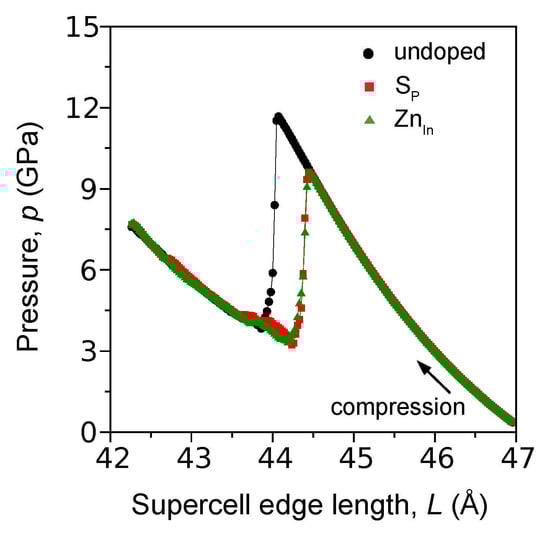
Figure 1.
Results of MD simulations showing pressure (p) versus supercell edge length (L) relationship obtained for undoped as well as Zn- and S-doped InP crystal. The sudden drop of the pressure indicates instability and transformation of the initial B3 phase to a high-pressure one. Doping by Zn or S decreases the pressure of the phase transformation.
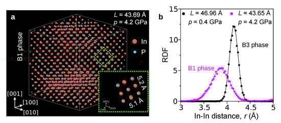
Figure 2.
Results of MD simulations presenting details of the high-pressure phase of undoped InP. (a) Inspection of the supercell right after the phase transformation shows atomic arrangement of the high-pressure phase. Visualization of the unit cell of the high-pressure phase proves that it possesses the B1 structure; (b) radial distribution function (RDF) calculated for In-In bonds. Location of the RDF peak facilitates estimation of the mean value of both B3 and B1 lattice constants.
Influence of and point defects on the structure of the B3 phase was first tested within the frame of DFT-based (Density Functional Theory) ab initio calculations (refer to Supplementary Materials). Substitution of Zn for the In atom creates Zn-P bonds characterized by the length Å, which is less than the In-P bond length in the undoped crystal : Å (contraction: ). In contrast, substitution of S for the P atom gives the bond In-S with the length Å (expansion: +0.039%). Based on these data, the parameters of the Lennard-Jones potential used for description of the interaction between the dopants and the atoms of InP crystal were determined (see Supplementary Materials). Despite the local strain sign, the presence of and point defects violates the order of the B3 lattice and decreases the pressure of the phase transformation (Figure 1 as well as Figure S2 in Supplementary Materials). The difference in the transformation pressure caused by the point defects is very small; therefore, we assumed a common value for the pressure of the transformation in Zn- as well as S-doped InP crystal: ( Å). The modeled decrease of the phase transformation pressure, from to , corresponds with the results of X-ray diffraction experiments accompanied by the Raman spectroscopy carried out for Fe-doped InP [].
The effect of and point defects on the generation of dislocations during nanoindentation of surface of InP can be demonstrated on the background of MD simulations performed for undoped crystal. Plastic deformation-preceded by formation of characteristic V-shaped shear-bands (see Figure S3 in Supplementary Materials)-starts at indentation depth Å (contact pressure ) when the first perfect dislocation (Figure 3a), characterized by the Burgers vector , appears beneath the indenter. Further increase of the indentation depth up to Å () results in development of the first perfect dislocation and generation of the second with a Burgers vector of , as presented in Figure 3b.
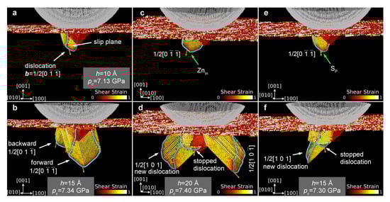
Figure 3.
Example results of MD simulations showing the effect of point defects on the development of dislocations during nanoindentation of the InP (001) surface. (a,b) Undoped InP: as indentation proceeds, the initial dislocation with the Burger vector develops and another dislocation (backward, ) is generated. (c,d) Zn-doped InP: the presence of Zn atom in front of the initial dislocation () stops its growth (well visible bending, pinning effect) and a new dislocations (, ) appear in the crystal. (e,f) S-doped InP: the presence of S atom acts in similar way, as in the case of Zn-doping. As a result, the development of existing dislocations is stopped. The increasing load can be accommodated by the emergence of new defects. The symbols h and denote the indentation depth and the instantaneous contact pressure value, respectively.
To show the impact of and point defects on the generation of dislocations, the simulations conducted for undoped InP were stopped when the indentation depth h reached the value of 10 Å and then the Zn or S atom was inserted into the place occupied by the In or P atom, respectively (Figure S4 in Supplementary Materials). The substitution was made on the slip plane of the first dislocation () but slightly further towards its development direction (Figure 3c,e and Figure S4 in Supplementary Materials). After that, the simulations were continued, and it turned out that the growth of the first dislocation () was stopped (pinning effect). Instead of its further development, an increase of the stress led to the creation of new dislocations with a Burgers vector of and (Figure 3d,f). This result demonstrates the phenomenon suggested by a result of the literature data analysis, which indicates that doping the InP causes an increase in microhardness [] as well as suppression of the dislocation generation during crystal growth [,]. The effect of doping on the development of dislocation structure is of stochastic nature, due to the thermal randomness of both the generation of dislocations and the location of point defects in a crystal lattice. However, when performing experiments with the nanoindentation method, it can be expected that the doping of the tested crystal will cause an increase in the mean value of the contact pressure at the beginning of plastic deformation, provided that the phenomenon initiating plasticity is dislocation nucleation. Indeed, as our simulations have shown, a point defect lying in the slip plane may stop the movement of dislocations and overcoming this obstacle or nucleating new dislocations will require an increase in stress.
The outcomes of our MD simulation made it possible to propose a method to determine the mechanism of nanoindentation-induced plastic deformation in InP. If the elastic-plastic transition is caused by the generation of dislocations, it could be expected that the doping increases the mean contact pressure at the onset of the plastic deformation. Moreover, if the elastic-plastic transition is caused by the phase transformation, the mean contact pressure should decrease due to doping.
To demonstrate the usefulness of the proposed method, we recall the results of nanoindentation experiments [] on Zn- and S-doped InP crystals characterized by the dopant concentrations and , respectively. For the sake of comparison, we also investigated Si-doped GaAs (), as it was already proved that the nanoindentation induced plasticity of GaAs starts from structural phase transformation () [,,]. We recorded numerous (∼400 for each sample, Figure 4) load (P) versus displacement (h) curves to determine the mean contact pressure at the elastic-plastic transition marked by the pop-in (discontinuity of the curve, details in Supplementary Materials). There was a significant shift of the contact pressure distributions recorded for InP towards higher values. The mean contact pressure at the onset of the elastic-plastic transition (pop-in) registered for undoped InP was with standard deviation (Figure 4a), while the values of pop-in measured for Zn and S doped crystal approached the values of and , respectively (Figure 4b,c). In light of our MD simulation, an increase in pop-in contact pressure indicates that the nanoindentation induced elastic-plastic transition in InP crystal is initiated by nucleation of dislocation. This is in contrast with the case of GaAs, for which a decrease of pop-in from to , caused by Si-doping, was measured (Figure 4d,e). In consequence, the nanoindentation induced elastic-plastic transition in GaAs is caused by the structural phase transformation.
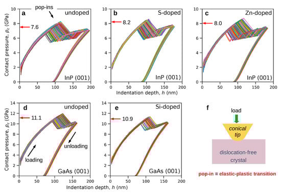
Figure 4.
Results of nanoindentation experiments on the InP surface: curves obtained for undoped (a) S- (b) and Zn-doped (c) crystals []. The red arrow assisted by the number indicates the mean contact pressure. Doping of InP shifts the mean contact pressure distribution towards higher values. In contrast, Si-doping of GaAs causes a decrease in the contact pressure (d,e). The last panel (f) presents a schematic of a nanoindentation experiment.
4. Conclusions
In summary, we used MD simulations to study the effect of doping on the pressure of phase transformation and dislocation generation in nanoindented InP. It was shown that the presence of impurities in the crystal lattice reduces the pressure of phase transformation and inhibits the development of the dislocation structure. Based on these results, we propose a simple method that allows for distinguishing the phenomenon that initiates nanoscale plasticity in semiconductor crystals. It indicates that the nanoindentation induced plasticity InP is initiated by the generation of dislocations, while the nanoscale plasticity of GaAs begins the structural phase transition. By showing that the method works for both InP and GaAs, we expect that application of the method to other semiconductors will allow for investigating the nature of their nanoscale plasticity.
Supplementary Materials
Supplementary data and figures are available online at https://www.mdpi.com/article/10.3390/ma14154157/s1.
Author Contributions
Conceptualization, D.C.; Methodology, D.C., G.Z. and A.C.; Validation, D.C., G.Z. and A.C.; Writing—original draft, D.C. and A.C. All authors have read and agreed to the published version of the manuscript.
Funding
This research was funded by the National Science Centre in Poland grant 2016/21/B/ST8/02737.
Institutional Review Board Statement
Not applicable.
Informed Consent Statement
Not applicable.
Data Availability Statement
The data presented in this study are available on request from the corresponding author.
Conflicts of Interest
The authors declare no conflict of interest.
References
- Wong, S.; Haberl, B.; Williams, J.S.; Bradby, J.E. Phase transformation as the single-mode mechanical deformation of silicon. Appl. Phys. Lett. 2015, 106, 252103. [Google Scholar] [CrossRef] [Green Version]
- Atwater, H.A.; Polman, A. Plasmonics for improved photovoltaic devices. Nat. Mater. 2010, 9, 205–213. [Google Scholar] [CrossRef] [PubMed]
- Clavero, C. Plasmon-induced hot-electron generation at nanoparticle/metal-oxide interfaces for photovoltaic and photocatalytic devices. Nat. Photonics 2014, 8, 95. [Google Scholar] [CrossRef]
- Chrobak, D.; Tymiak, N.; Beaber, A.; Ugurlu, O.; Gerberich, W.W.; Nowak, R. Deconfinement leads to changes in the nanoscale plasticity of silicon. Nat. Nanotechnol. 2011, 6, 480–484. [Google Scholar] [CrossRef]
- Wong, S.; Haberl, B.; Williams, J.S.; Bradby, J.E. The influence of hold time on the onset of plastic deformation in silicon. J. Appl. Phys. 2015, 118, 245904. [Google Scholar] [CrossRef]
- Gerbig, Y.B.; Michaels, C.A.; Forster, A.M.; Cook, R.F. In situ observation of the indentation-induced phase transformation of silicon thin films. Phys. Rev. B 2012, 85, 104102. [Google Scholar] [CrossRef] [Green Version]
- Gerbig, Y.B.; Michaels, C.A.; Cook, R.F. In situ observation of the spatial distribution of crystalline phases during pressure-induced transformations of indented silicon thin films. J. Mater. Res. 2015, 30, 390–406. [Google Scholar] [CrossRef]
- Gerbig, Y.B.; Michaels, C.A.; Cook, R.F. In situ observations of Berkovich indentation induced phase transitions in crystalline silicon films. Scr. Mater. 2016, 120, 19–22. [Google Scholar] [CrossRef] [PubMed] [Green Version]
- Chrobak, D.; Nordlund, K.; Nowak, R. Nondislocation Origin of GaAs Nanoindentation Pop-In Event. Phys. Rev. Lett. 2007, 98, 045502. [Google Scholar] [CrossRef] [PubMed]
- Nowak, R.; Chrobak, D.; Nagao, S.; Vodnick, D.; Berg, M.; Tukiainen, A.; Pessa, M. An electric current spike linked to nanoscale plasticity. Nat. Nanotechnol. 2009, 4, 287–291. [Google Scholar] [CrossRef] [PubMed]
- Chrobak, D.; Raisanen, J.; Nowak, R. Effect of silicon on the elastic–plastic transition of GaAs crystal. Scr. Mater. 2015, 102, 31–34. [Google Scholar] [CrossRef]
- Fujikane, M.; Inoue, A.; Yokogawa, T.; Nagao, S.; Nowak, R. Mechanical properties characterization of c -plane (0001) and m -plane (10–10) GaN by nanoindentation examination. Phys. Status Solidi C 2010, 7, 1798–1800. [Google Scholar] [CrossRef]
- Fujikane, M.; Yokogawa, T.; Nagao, S.; Nowak, R. Nanoindentation study on insight of plasticity related to dislocation density and crystal orientation in GaN. Appl. Phys. Lett. 2012, 101, 201901. [Google Scholar] [CrossRef]
- Chrobak, D.; Chrobak, A.; Nowak, R. Effect of doping on nanoindentation induced incipient plasticity in InP crystal. AIP Adv. 2019, 9, 125323. [Google Scholar] [CrossRef] [Green Version]
- Chrobak, D.; Trebala, M.; Chrobak, A.; Nowak, R. Origin of Nanoscale Incipient Plasticity in GaAs and InP Crystal. Crystals 2019, 9, 651. [Google Scholar] [CrossRef] [Green Version]
- Bourhis, E.L.; Riviere, J.P.; Zozime, A. Material flow under an indentor in indium phosphide. J. Mater. Sci. 1996, 31, 6571–6576. [Google Scholar] [CrossRef]
- Patriarche, G.; Bourhis, E.L. In-depth deformation of InP under a Vickers indentor. J. Mater. Sci. 2001, 36, 1343–1347. [Google Scholar] [CrossRef]
- Jian, S.R.; Jang, J.S.C. Berkovich nanoindentation on InP. J. Alloys Compd. 2009, 482, 498–501. [Google Scholar] [CrossRef]
- Wasmer, K.; Gassilloud, R.; Michler, J.; Ballif, C. Analysis of onset of dislocation nucleation during nanoindentation and nanoscratching of InP. J. Mater. Res. 2012, 27, 320–329. [Google Scholar] [CrossRef] [Green Version]
- Almeida, C.M.; Prioli, R.; Wei, Q.Y.; Ponce, F.A. Early stages of mechanical deformation in indium phosphide with the zinc blende structure. J. Appl. Phys. 2012, 112, 063514. [Google Scholar] [CrossRef]
- Chiu, Y.J.; Jian, S.R.; Liu, T.J.; Le, P.H.; Juang, J.Y. Localized Deformation and Fracture Behaviors in InP Single Crystals by Indentation. Micromachines 2018, 9, 611. [Google Scholar] [CrossRef] [Green Version]
- Plimpton, S. Fast Parallel Algorithms for Short-Range Molecular Dynamics. J. Comput. Phys. 1995, 117, 1–19. [Google Scholar] [CrossRef] [Green Version]
- Physical Properties of Selected Semiconductors. Available online: http://www.ioffe.ru/SVA/NSM/Semicond/InP (accessed on 26 July 2021).
- Arivuoli, D.; Fornari, R.; Kumar, J. Microhardness studies of doped and undoped InP crystals. J. Mater. Sci. Lett. 1991, 10, 559–561. [Google Scholar] [CrossRef]
- Branicio, P.S.; Rino, J.P.; Shimojo, F. High-pressure phases of InP: An ab initio and molecular-dynamics study. Appl. Phys. Lett. 2006, 88, 161919. [Google Scholar] [CrossRef]
- Branicio, P.S.; Rino, J.P.; Gan, C.K.; Tsuzuki, H. Interaction potential for indium phosphide: A molecular dynamics and first-principles study of the elastic constants, generalized stacking fault and surface energies. J. Phys. Condens. Matter 2009, 21, 095002. [Google Scholar] [CrossRef]
- Stukowski, A. Visualization and analysis of atomistic simulation data with OVITO–the Open Visualization Tool. Model. Simul. Mater. Sci. Eng. 2010, 18, 015012. [Google Scholar] [CrossRef]
- Menoni, C.S.; Spain, I.L. Equation of state of InP to 19 GPa. Phys. Rev. B 1987, 35, 7520–7525. [Google Scholar] [CrossRef] [PubMed]
- Nelmes, R.; McMahon, M. Chapter 3 Structural Transitions in the Group IV, III–V, and II–VI Semiconductors under Pressure. In Semiconductors and Semimetals; Academic Press: San Diego, CA, USA, 1998; Volume 54, pp. 145–246. [Google Scholar] [CrossRef]
- Mujica, A.; Rubio, A.; Munoz, A.; Needs, R.J. High-pressure phases of group-IV, III–V, and II–VI compounds. Rev. Mod. Phys. 2003, 75, 863–912. [Google Scholar] [CrossRef] [Green Version]
- Lin, C.M.; Hsu, I.J.; Lin, S.C.; Chuang, Y.C.; Chen, W.T.; Liao, Y.F.; Juang, J.Y. Pressure effect on impurity local vibrational mode and phase transitions in n-type iron-doped indium phosphide. Sci. Rep. 2018, 8, 1284. [Google Scholar] [CrossRef] [PubMed] [Green Version]
- Bose, D.N.; Seishu, B.; Parthasarathy, G.; Gopal, E.S.R. Doping dependence of semiconductor–metal transition in InP at high pressures. Proc. R. Soc. Lond. A 1986, 405, 345–353. [Google Scholar] [CrossRef]
- Roksnoer, P.J.; Boom, M.M.B.V.R.V.D. The single crystal growth and characterization of indium phosphide. J. Cryst. Growth 1984, 66, 317–326. [Google Scholar] [CrossRef]
- Oda, O.; Katagiri, K.; Shinohara, K.; Katsura, S.; Takahashi, Y.; Kainosho, K.; Kohiro, K.; Hirano, R. Chapter 4 InP Crystal Growth, Substrate Preparation and Evaluation. In Semiconductors and Semimetals; Academic Press: San Diego, CA, USA, 1990; Volume 31, pp. 93–174. [Google Scholar] [CrossRef]
Publisher’s Note: MDPI stays neutral with regard to jurisdictional claims in published maps and institutional affiliations. |
© 2021 by the authors. Licensee MDPI, Basel, Switzerland. This article is an open access article distributed under the terms and conditions of the Creative Commons Attribution (CC BY) license (https://creativecommons.org/licenses/by/4.0/).