Abstract
The properties of Al-doped SnOx films deposited via reactive co-sputtering were examined in terms of their potential applications for the fabrication of transparent and flexible electronic devices. Al 2.2-atom %-doped SnOx thin-film transistors (TFTs) exhibit improved semiconductor characteristics compared to non-doped films, with a lower sub-threshold swing of ~0.68 Vdec−1, increased on/off current ratio of ~8 × 10⁷, threshold voltage (Vth) near 0 V, and markedly reduced (by 81%) Vth instability in air, attributable to the decrease in oxygen vacancy defects induced by the strong oxidizing potential of Al. Al-doped SnOx films maintain amorphous crystallinity, an optical transmittance of ~97%, and an adhesive strength (to a plastic substrate) of over 0.7 kgf/mm; such films are thus promising semiconductor candidates for fabrication of transparent flexible TFTs.
1. Introduction
In recent years, intensive research efforts have focused on metal oxide semiconductors, such as ZnO, SnO2, In2O5, and InGaZnO5, which have many applications in electronics, sensors, and active matrix displays. Because of their high electron mobility and good transparency, metal oxide semiconductors are especially ideal candidates for the active layers of thin-film transistors (TFTs) [1,2,3,4,5,6,7]. Most metal oxide semiconductors are fabricated via sputtering; their properties are determined by reactions between the injected gases (Ar and O2) and the metals (e.g., In, Sn, Zn, and Ga), typically yielding amorphous, conductive, and transparent materials. Especially compared to amorphous silicon, metal oxide semiconductors can be fabricated at a relatively low temperature (≤300 °C), even room temperature, and have higher electron mobility than amorphous silicon, thus finding many applications in the manufacture of organic light-emitting diode display panels.
However, metal oxide semiconductors have a problem of stability, because of oxygen deficiencies and reaction with the external environment. The high electron carrier level caused by oxygen vacancies also compromises semiconductor device controllability. Therefore, it is very important to reduce oxygen vacancy defects. If a doped component could maintain the oxygen content in the metal oxide semiconductors, the device stability and controllability would improve [8].
Here, we fabricated Al-doped SnOx films via sputtering and explored the effect of the Al doping on SnOx films on electrical, structural, and optical properties. We further fabricated TFTs to investigate their transfer characteristics and stability. In addition, we used a simple peel test to estimate adhesion between Al-doped SnOx thin films and flexible plastic substrates at different Al contents, which would be critical to flexible device fabrication [9,10,11].
2. Materials and Methods
Bottom gate TFTs based on Al-doped SnOx were fabricated. Highly doped Si (P++) and thermally grown SiO2 (100 nm) served as the gate electrode and insulator, respectively. As a channel layer, 10 nm thick SnO2 films were deposited using radiofrequency (RF) reactive magnetron sputtering. For Al doping of SnO2, co-sputtering was performed using Sn (99.999%) and Al (99.999%) targets and an O2/Ar gas mixture (O2:Ar = 1:3). To explore the effects of doping, the input RF power of the Al target was varied from 0 to 100 and 200 W (yielding TFTs termed SO, ASO1, and ASO2, respectively), whereas that of the Sn target was fixed at 200 W. The channel thickness of all three samples was fixed at 10 nm, as confirmed using a spectroscopic ellipsometer (MG-1000, Nano-View Co., Ansan, Korea) and a field effect scanning electron microscope (S5300, Hitachi Inc., Tokyo, Japan). The source/drain electrodes were 10 wt % Sn-doped In2O3 (indium tin oxide), deposited via direct-current magnetron sputtering at 200 W to a thickness of 100 nm. 1000 μm wide and 100 μm long channel patterns were created using a shadow mask. Sputtering was performed at a base pressure of 1 × 10⁻⁶ Torr and a working pressure of 10 mTorr at room temperature. The TFTs were subjected to thermal annealing at 150 °C for 1 h in air using a quartz tube furnace. The electrical performance of the Al-doped SnOx TFTs was measured using an HP4145B semiconductor analyzer operating at room temperature in the dark. In addition, we measured changes in TFT transfer characteristics over time. TFTs without passivation layers were exposed to the air at room temperature under dehumidifying condition. The chemical compositions and Sn-bonding states of the Al-doped SnOx thin films were analyzed by X-ray photoelectron spectroscopy (XPS) (Multilab 2000, Thermo Scientific Ltd., Waltham, MA, USA). The atomic percentage of each element in the films was calculated by dividing the area under the curve by the relative sensitivity factor for each peak at C 1s, Al 2p, Sn 3d, and O 1s XPS spectra and normalizing the values over the total amount of the elements in the films. Carrier densities were measured using the Hall method (HMS-5300, Ecopia, Anyang, Korea), employing the Van der Pauw configuration. Crystallinity was evaluated via high-resolution X-ray diffraction (HR-XRD), during which Cu Kα radiation was delivered at a glancing angle (D8 Discover, Bruker AXS Ltd., Karlsruhe, Germany). Optical transmittance was assessed with the aid of a UV-visible spectrophotometer (UV-2450, Shimadzu Corp., Tokyo, Japan). A peel tester stand (AD4935-50N, And Inc., Tokyo, Japan) and duct tape (GT2, 3M Espe, Maplewood, NJ, USA) were used to measure adhesion between the Al-doped SnOx thin films and the polyimide (PI) films. Samples were fixed to glass to prevent cracking during bending or handling. Changes in sheet resistance after the peel test were analyzed via four-point probing using a source meter (2400, Keithley Inc., Beaverton, AL, USA) to evaluate adhesion between the Al-doped SnOx thin films and the PI films.
3. Results and Discussions
3.1. Electrical Characterization of Al-Doped SnOx Thin-Film Transistors
Figure 1 shows the transfer characteristics of SO, ASO1, and ASO2, which were scanned with forward (−20 V → +20 V) and reverse (+20 V → −20 V) bias sweeps. The source and drain voltages (VD) were the constant ground voltage and 10.1 V, respectively. The threshold voltage (Vth) was the voltage evident when the current approached L/W × 10 nA [12]. The saturation mobility (μsat) and subthreshold swing (SS) were 2L/WCi × (dID1/2/dVG)2 and (dlog ID/dVG)−1 respectively, where Ci is the capacitance per unit area of the gate dielectric (34.5 nF/cm2) [13,14,15]. The Vth, Ion/Ioff, μsat, SS, and Al atomic concentrations (in atom %) of SO, ASO1, and ASO2 are listed in Table 1. The Al atomic percentage values were evaluated via XPS spectral analysis, assuming that the films consisted of C, Al, Sn, and O. As shown in Figure 1, the TFT device exhibited n-type conduction. Although SnO2 is a well-known n-type material, several papers have reported that Al-incorporated SnOx showed p-type semiconducting behavior. This is due to the hole carriers produced by the Al3+-Sn4+ substitution reaction when the Al concentration exceeds 5% in a SnO2 film [16,17]. Therefore, it is possible the n-type behavior of the TFT may be caused by the low concentration (≤2.24%) of Al, which is not enough to make holes majority carriers in SnOx films. As the extent of Al doping increased, Vth changed from −13.4 to −1.0 V, thus becoming close to 0 V, and the Ion/Ioff ratio increased dramatically (over 25-fold) because the off-current was much lower than that of undoped SnOx. Chu et al. reported that reduced carrier concentration in the n-type channel material induces higher Vth and lower Ioff, because the channel with lower carrier concentration is more easily depleted [18]. Therefore, these positive shifts of Vth and decreased Ioff are attributable to reductions in electron density in the TFT channels as Al levels increase [2,6,18,19]. In general, oxygen vacancies in SnOx-based materials generate free electrons, which is accompanied by n-type semiconduction [20,21]. The standard oxidization potential (at 25 °C) of Al is higher than that of Sn by 1.37 V; Al is thus a stronger oxidizer than Sn [22]. Hence, if enough oxygen is supplied during the sputtering process, fewer oxygen vacancies are induced in Al-doped SnOx layers compared to non-doped SnOx, because the film oxygen content is higher given the stronger oxidizing power of Al. Consequently, decreasing electron density with increasing Al content in the film could be attributed to fewer oxygen vacancies in the ASO1 and ASO2 channels due to the strong oxidizing potential of Al, resulting in the increased Vth and Ion/Ioff ratio. Moreover, the insulating property of Al2O3, which was formed during the RF sputtering process in the Ar/O2 ambience, could be another reason for lower electron density compared to non-doped SnOx layer. Hall measurements confirmed the reductions in electron density, which were 9.41 × 1018 cm−3 for SO and 6.09 × 1015 cm−3 for ASO2. The μsat (2.27 ± 0.03 cm2 V−1 s−1) did not change significantly after doping, which was also confirmed by the similar slope in Figure S1 in the supplementary material. However, the SS of ASO2 fell to 0.68 V dec.−1, less than 33% of that of SO, further improving TFT performance. Clockwise hysteresis was observed, and revealed that electron traps existed at or near the channel/insulator interface. The hysteresis (|ΔVth|) of ASO2 was decreased to 1.13 V, much less than that of SO (2.67 V), which indicates that the hysteresis can be obviously suppressed by Al doping.
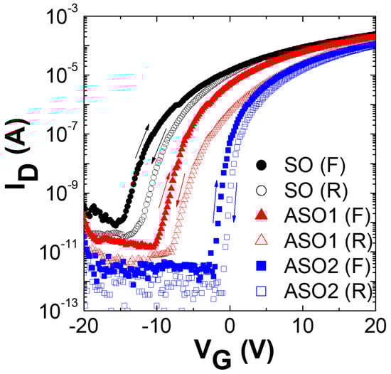
Figure 1.
Transfer curves of the SO, ASO1 and ASO2 thin-film transistors (TFTs) containing Al at atom % values of 0, 1.20, and 2.24, which were scanned with forward (F) and reverse (R) bias sweeps (VD = 10.1 V).

Table 1.
Electrical parameters revealed by the thin-film transistor (TFT) transfer curves scanned with forward bias sweep, hysteresis (H) in clockwise direction and Al atomic concentrations from X-ray photoemission spectroscopy (XPS) spectral analyses.
We explored changes in TFT transfer characteristics over time (Figure 2). VG-ID curves were drawn daily for 2 weeks after TFT fabrication; the Vth values gradually became more positive because the channels absorbed atmospheric oxygen [23,24]. After 14 days, the Vth values of SO, ASO1, and ASO2 had shifted by 6.2, 4.2, and 1.2 V, respectively, indicating that the ambient stability of SnOx film can be improved by Al doping. Yan et al. reported that oxygen adsorption is preferred on oxygen-deficient surfaces, and that molecular oxygen can heal oxygen vacancies in the oxide material [25]. Therefore, this decreased Vth shift with increasing Al content is attributable to the reduced reaction between the surfaces of the channels and the oxygen in the atmosphere, because Al-doped channels have fewer oxygen vacancies than undoped channels, as discussed in Figure 1.
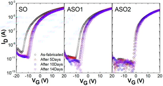
Figure 2.
Changes in the transfer characteristics of SO, ASO1, and ASO2 TFTs (lacking passivation layers) over time.
3.2. Structural and Optical Properties of Al-Doped SnOx Thin-Films
In order to support the electrical characteristics of the TFTs, we performed analyses of structural and optical properties of SnOx thin films with different Al concentrations. Figure 3a shows the Sn 3d5/2 XPS spectra of the SO, SAO1, and SAO2 films. The Sn 3d5/2 peaks were deconvoluted into two sub-peaks with binding energies of 487.0 and 486.3 eV [19,26], respectively, corresponding to the Sn4+ and Sn2+ binding states. The Sn2+ peak area clearly decreased with the Al proportion, while that of the Sn4+ peak increased. The relative peak intensity [Sn2+/Sn4+ + Sn2+] of the Sn2+ peak fell from 0.37 to 0.16 with increasing Al doping (Figure 3b). Huh et al. found that Sn2+ binding in SnO2 caused oxygen vacancy defects [19]. Moreover, the O 1s peaks were deconvoluted into two sub-peaks corresponding to the lattice oxygen (OL) and oxygen deficiency (OD), located at 530.9 and 531.3 eV [2,27] respectively, as shown in Figure 3c. As the Al doping increases, the reduction of OD peak area can be evidently observed, as confirmed in Figure 3d, which shows the decrease of the relative peak intensity [OD/OL+OD] of OD peak from 0.22 to 0.18 with increasing Al concentration. Therefore, the reductions in the proportions of the Sn2+ and OD peaks with Al content reflect the reductions in electron density and oxygen vacancies; the channels operate efficiently at increasingly higher Ion/Ioff ratios and reduced SS, and are more stable in air (see also Figure 1 and Figure 2).
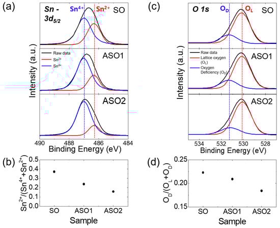
Figure 3.
(a) Sn 3d5/2 X-ray photoemission spectroscopy (XPS) spectra of SO, ASO1, and ASO2 thin-films. (b) Relative peak intensities [Sn2+/Sn4+ + Sn2+] of the Sn2+ peaks. (c) O 1s XPS spectra of SO, ASO1, and ASO2 thin films. (d) Relative peak intensities of [OD/(OL + OD)] of the OD peaks.
Next, SO, ASO1, and ASO2 thin films formed on Si/SiO2 (100 nm) substrates were subjected to glancing-angle HR-XRD to evaluate crystallinity changes (Figure 4). The samples were prepared with the thickness of 20 nm to ensure that, if present, diffraction peaks would be evident, and annealed at 150 °C for 1 h. All samples were amorphous, lacking the diffraction peaks identified earlier [19,28]. This means our films have high areal uniformity for device characteristics, which is essential for fabricating devices on large-scale substrate [1]. To evaluate optical properties, 10 nm thick films were deposited on glass. As shown in Figure 5, all visible (λ = 390~700 nm) optical transmittances were >97%, and optical band-gaps determined by extrapolating the best fit to the intercept (at α = 0) in the Tauc plot [2,29] were ~3.5 eV plot for all samples, as required for fabrication of transparent electronic devices.
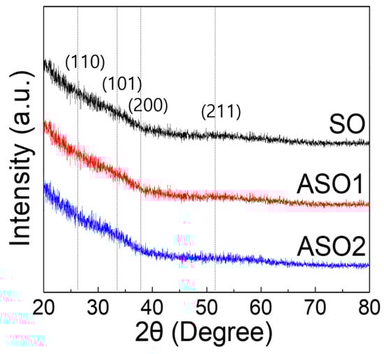
Figure 4.
High resolution X-ray diffraction (HR-XRD) patterns of SO, SAO1, and SAO2 thin-films with different Al concentrations.
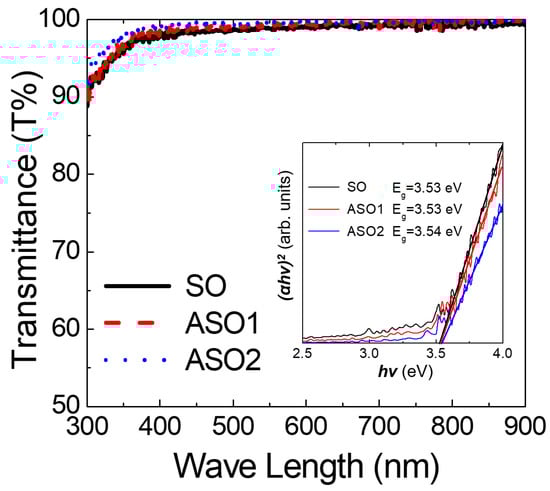
Figure 5.
Optical transmittance values as a function of wavelength and (inset) Tauc plot as a function of photon energy (hν) for the SO, ASO1, ASO2 thin films with different Al concentrations.
3.3. Adhesive Property between Al-Doped SnOx Thin-Films and Plastic Substrate
We used the peel test to investigate the adhesion between the Al-doped SnOx thin-films and PI substrates that are known to be stable below 260 °C. 10 nm thick SO, ASO1, and ASO2 thin films were RF-sputtered onto pre-cleaned PI and annealed at 150 °C. The peel test was performed using duct tape with an adhesion strength ≥ 0.7 kgf/mm (as revealed by a 180° peel test using the samples and the tape). The tape remained perfectly bonded to the SO, ASO1, and ASO2 surfaces under a vertical load of 5 kg, and was then detached. Figure 6 shows the sheet resistance values before and after the peel test. For the SO, ASO1 and ASO2 films, these were ~177, ~4613 and ~89,742 kΩ/sq. prior to the peel test, respectively. The sheet resistance of fabricated samples gradually increased with increasing Al content, attributable to the decreased carrier concentrations and improved semiconductor characteristics (see Figure 1). No significant change was evident after the peel test. If peeling occurred at the interface between a thin film and the polymer substrate, the film sheet resistance would increase. Although we did not measure the maximal adhesive strength, this was >0.7 kgf/mm, thus above the adhesive strength of duct tape.
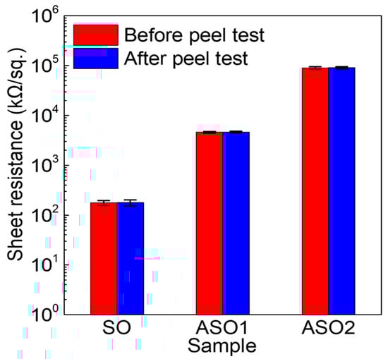
Figure 6.
Sheet resistance changes before and after the peel test for SO, ASO1, and ASO2 thin films on a polyimide (PI) substrate.
4. Conclusions
We fabricated SnOx-based TFTs doped with different levels of Al via RF reactive co-sputtering. Compared to SnOx, the Al-doped films exhibited improved channel semiconductor characteristics, including a shift in Vth to almost 0 V, an increased Ion/Ioff ratio, a reduced SS, and improved stability in air, which are attributable to the reduced oxygen deficiencies (because Al is a stronger oxidizer than Sn). The oxygen deficiency reduction by Al doping was confirmed by the decrease of Sn2+ and OD proportion in Sn 3d5/2 and O 1s XPS spectral analysis. The Al-doped SnOx films are amorphous and have an optical transmittance of ~97% and an adhesive strength (to PI) of >0.7 kgf/mm, which facilitates their use in flexible and transparent electronics.
Supplementary Materials
The following are available online at http://www.mdpi.com/1996-1944/12/1/137/s1, Figure S1: The (IDS)1/2 versus VG curves of SO, ASO1, and ASO2 TFTs for comparison of electron mobilities at VD = 10.1V.
Author Contributions
S.-H.L., K.K. (Kihwan Kwon), Y.Y., S.K. and J.H.K. conceived and designed the experiments; S.-H.L. and J.H.K. performed the experiments; S.-H.L., K.K. (Kihwan Kwon), K.K. (Kwanoh Kim), J.S.Y., Y.Y., C.K., S.K. and J.H.K. analyzed the data; D.-S.C., Y.Y contributed materials/analysis tools; S.-H.L. prepared original draft; J.H.K. revised the manuscript.
Funding
The research was supported by a National Research Foundation of Korea (NRF) grant funded by the Ministry of Science and ICT for the First-Mover Program for Accelerating Disruptive Technology Development (NRF-2018M3C1B9069841). The work was also funded by Korea Institute of Machinery and Materials (NK211D).
Conflicts of Interest
The authors declare no conflict of interest.
References
- Nomura, K.; Ohta, H.; Takagi, A.; Kamiya, T.; Hirano, M.; Hosono, H. Room-temperature fabrication of transparent flexible thin-film transistors using amorphous oxide semiconductors. Nature 2004, 432, 488–492. [Google Scholar] [CrossRef] [PubMed]
- Kim, J.I.; Ji, K.H.; Jang, M.; Yang, H.; Choi, R.; Jeong, J.K. Ti-doped indium tin oxide thin films for transparent field-effect transistors: Control of charge-carrier density and crystalline structure. ACS Appl. Mater. Interfaces 2011, 3, 2522–2528. [Google Scholar] [CrossRef]
- Fortunato, E.M.C.; Barquinha, P.M.C.; Pimentel, A.C.M.B.G.; Concalves, A.M.F.; Marques, A.J.S.; Pereira, L.M.N.; Martins, R.F.P. Fully Transparent ZnO thin-film transistor produced at room temperature. Adv. Mater. 2005, 17, 590–594. [Google Scholar] [CrossRef]
- Maiolo, L.; Mirabella, S.; Maita, F.; Alberti, A.; Minotti, A.; Strano, V.; Pecora, A.; Shacham-Diamand, Y.; Fortunato, G. Flexible pH sensors based on polysilicon thin film transistor and ZnO nanowalls. Appl. Phys. Lett. 2014, 105, 093501. [Google Scholar] [CrossRef]
- Kim, H.Y.; Jung, E.A.; Mun, G.; Agbenteke, R.E.; Park, B.K.; Park, J.S.; Son, S.U.; Jeon, D.J.; Park, S.H.K.; Chang, T.M.; et al. Low-temperature growth of indium oxide thin film by plasma-enhanced atomic layer deposition using liquid dimethyl(N-ethoxy-2,2-dimethylpropanamido)indium for high-mobility thin film transistor application. ACS Appl. Mater. Interfaces 2016, 8, 26924–26931. [Google Scholar] [CrossRef]
- Sheng, J.; Jeong, H.-J.; Han, K.-L.; Hong, T.H.; Park, J.-S. Review of recent advances in flexible oxide semiconductor thin-film transistors. J. Inf. Disp. 2017, 18, 159–172. [Google Scholar] [CrossRef]
- Lee, H.; Zhang, X.; Kim, J.W.; Kim, E.-J.; Park, J. Investigation of the Electrical Characteristics of Bilayer ZnO/In2O3 Thin-Film Transistors Fabricated by Solution Processing. Materials 2018, 11, 2013. [Google Scholar] [CrossRef]
- Minami, T.; Miyata, T.; Ohtani, Y.; Kuboi, T. Effect of thickness on the stability of transparent conducting impurity-doped ZnO thin films in a high humidity environment. Phys. Status Solidi RRL 2007, 1, R31–R33. [Google Scholar] [CrossRef]
- Lewis, J. Material challenge for flexible organic devices. Mater. Today 2006, 9, 39–45. [Google Scholar] [CrossRef]
- Ramos, M.M.D. Theoretical study of metal-polyimide interfacial properties. Vacuum 2002, 64, 255–260. [Google Scholar] [CrossRef]
- Hull, T.R.; Colligon, J.S.; Hill, A.E. Measurement of thin film adhesion. Vacuum 1987, 37, 327–330. [Google Scholar] [CrossRef]
- Lee, C.-K.; Park, S.Y.; Jung, H.Y.; Lee, C.K.; Son, B.-G.; Kim, H.J.; Lee, Y.-J.; Joo, Y.-C.; Jeong, J.K. High performance Zn-Sn-O thin film transistors with Cu Source/drain electrode. Phys. Status Solidi RRL 2013, 7, 196–198. [Google Scholar] [CrossRef]
- Hamilton, M.C.; Martin, S.; Kanicki, J. Field-effect mobility of organic polymer thin-film transistors. Chem. Mater. 2004, 16, 4699–4704. [Google Scholar] [CrossRef]
- Li, J.; Ding, X.-W.; Zhang, J.-H.; Zhang, H.; Jiang, W.-Y.; Zhang, Z.-L. Improving electrical performance and bias stability of HfInZnO-TFT with optimizing the channel thickness. AIP Adv. 2013, 3, 102132. [Google Scholar] [CrossRef]
- Han, S.J.; Kim, S.; Ahn, J.; Jeong, J.K.; Yang, H.; Kim, H.J. Composition-dependent structural and electrical properties of p-type SnOx thin films prepared by reactive DC magnetron sputtering: Effects of oxygen pressure and heat treatment. RSC Adv. 2016, 6, 71757–71766. [Google Scholar] [CrossRef]
- Lee, P.-M.; Liu, Y.-S.; Villamagua, L.; Stashans, A.; Carini, M.; Liu, C.-Y. Experimental observation and computer simulation of Al/Sn substitution in p-type aluminum nitride-doped tin oxide thin film. J. Phys. Chem. C 2016, 120, 4211–4218. [Google Scholar] [CrossRef]
- Ahmed, S.F.; Khan, S.; Ghosh, P.K.; Mitra, M.K.; Chattopadhyay, K.K. Effect of Al doping on the conductivity type inversion and electro-optical properties of SnO2 thin films synthesized by sol-gel technique. J. Sol-Gel Sci. Technol. 2006, 39, 241–247. [Google Scholar] [CrossRef]
- Chu, H.-C.; Shen, Y.-S.; Hsieh, C.-H.; Huang, J.-H.; Wu, Y.-H. Low-voltage operation of ZrO2-gated n-type thin film transistors based on a channel formed by hybrid phases of SnO and SnO2. ACS Appl. Mater. Interfaces 2015, 7, 15129–15137. [Google Scholar] [CrossRef]
- Huh, M.S.; Yang, B.S.; Oh, S.; Yoon, K.; Jeong, J.K.; Hwang, C.S.; Kim, H.J. Improvement in the Performance of Tin Oxide Thin-Film Transistors by Alumina Doping. Electochem. Solid-State Lett. 2009, 12, H385–H387. [Google Scholar] [CrossRef]
- Saji, K.J.; Mary, A.P.R. Tin oxide based P and N-type thin film transistors developed by RF sputtering. ECS J. Solid State Sci. Technol. 2015, 4, Q101–Q104. [Google Scholar] [CrossRef]
- Lee, B.K.; Jung, E.; Kim, S.H.; Moon, D.C.; Lee, S.S.; Park, B.K.; Hwang, J.H.; Chung, T.M.; Kim, C.G.; An, K.S. Physical/chemical properties of tin oxide thin film transistors prepared using plasma-enhanced atomic layer deposition. Mater. Res. Bull. 2012, 47, 3052–3055. [Google Scholar] [CrossRef]
- Lide, D.R. CRC Handbook of Chemistry and Physics, 87th ed. J. Am. Chem. Soc. 2007, 129, 724. [Google Scholar] [CrossRef]
- Jeong, J.K. The status and perspectives of metal oxide thin-film transistors for active matrix flexible displays. Semicond. Sci. Technol. 2011, 26, 034008. [Google Scholar] [CrossRef]
- Chong, E.; Chun, Y.S.; Kim, S.H.; Lee, S.Y. Effect of oxygen on the threshold voltage of a-IGZO TFT. J. Electr. Eng. Technol. 2011, 6, 539–542. [Google Scholar] [CrossRef]
- Yan, Y.; Al-Jassim, M.M.; Wei, S.-H. Oxygen-vacancy mediated adsorption and reaction of molecular oxygen on the ZnO (10-10) surface. Phys. Rev. B 2005, 72, 161307. [Google Scholar] [CrossRef]
- Moulder, J.F.; Stickle, W.F.; Sobol, P.E.; Bomben, K.D. Handbook of X-ray Photoelectron Spectroscopy, 1st ed.; Perkin-Elmer: Minnesota, MN, USA, 1992; p. 127. ISBN 978-0-96-270262-4. [Google Scholar]
- Jaiswar, S.; Mandal, K.D. Evidence of enhanced oxygen vacancy defects inducing ferromagnetism in multiferroic CaMn7O12 manganite with sinteing time. J. Phys. Chem. C 2017, 121, 19586–19601. [Google Scholar] [CrossRef]
- Nguyen, A.H.-T.; Nguyen, M.-C.; Choi, J.; Han, S.; Kim, J.; Choi, R. Electrical performance enhancement of p-type tin oxide channel thin film transistor using aluminum doping. Thin Solid Films 2017, 641, 24–27. [Google Scholar] [CrossRef]
- Wang, B.; Yu, X.; Guo, P.; Huang, W.; Zeng, L.; Zhou, N.; Chi, L.; Bedzyk, M.J.; Chang, R.P.H.; Marks, T.J.; et al. Solution-processed all-oxide transparent high-performance transistors fabricated by spray-combustion synthesis. Adv. Electron. Mater. 2016, 2, 1500427. [Google Scholar] [CrossRef]


© 2019 by the authors. Licensee MDPI, Basel, Switzerland. This article is an open access article distributed under the terms and conditions of the Creative Commons Attribution (CC BY) license (http://creativecommons.org/licenses/by/4.0/).