Abstract
The growing attention on plug-in electric vehicles, and the associated high-performance demands, have initiated a development trend towards highly efficient and compact on-board battery chargers. These isolated ac-dc converters are most commonly realized using two conversion stages, combining a non-isolated power factor correction (PFC) rectifier with an isolated dc-dc converter. This, however, involves two loss stages and a relatively high component count, limiting the achievable efficiency and power density and resulting in high costs. In this paper, a single-stage converter approach is analyzed to realize a single-phase ac-dc converter, combining all functionalities into one conversion stage and thus enabling a cost-effective efficiency and power density increase. The converter topology consists of a quasi-lossless synchronous rectifier followed by an isolated dual active bridge (DAB) dc-dc converter, putting a small filter capacitor in between. To show the performance potential of this bidirectional, isolated ac-dc converter, a comprehensive design procedure and multi-objective optimization with respect to efficiency and power density is presented, using detailed loss and volume models. The models and procedures are verified by a 3.7 kW hardware demonstrator, interfacing a 400 V dc-bus with the single-phase 230 V, 50 Hz utility grid. Measurement results indicate a state-of-the-art efficiency of 96.1% and power density of 2 kW/dm, confirming the competitiveness of the investigated single-stage DAB ac-dc converter.
1. Introduction
1.1. Overview and Objectives
Single-phase utility-interfaced ac-dc converters with power factor correction (PFC) and galvanic isolation cover a wide range of applications such as chargers for plug-in hybrid electrical vehicles (PHEVs) and battery electric vehicles (BEVs) [1,2], interfaces for residential dc distribution systems and energy storage systems [3,4], and inverters for photovoltaic modules. Bidirectional power flow is increasingly required since the traditional electricity grid is evolving towards a smart interactive service network (customers/operators) in which energy systems play an active role in providing different types of support to the grid [5], e.g., vehicle-to-grid (V2G) concepts [6].
The above mentioned isolated ac-dc converters are most commonly realized using a dual-stage (2-S) approach, involving a non-isolated power factor correction (PFC) rectifier, followed by a dc-link to which a high-frequency (HF) isolated dc-dc converter is connected. An extensive review of uni- and bidirectional single-phase PFC rectifier topologies with improved power quality is presented in [7], including some variants with galvanic isolation. Examples of soft-switched, single-phase, non-isolated, bidirectional PFC rectifiers are the boost-type PFC with passive snubber cell presented in [8] and the multi-cell totem-pole PFC described in [9,10], which employs a triangular current mode (TCM) modulation scheme. Extensive overviews, topology surveys, analyses, and comparative evaluations of common topologies used for the isolated dc-dc converter stage are presented in [11,12,13,14,15,16,17,18], inter alia including numerous (soft-switching) dual active bridge (DAB) topologies and resonant topologies, whether or not combined with active auxiliary snubber circuits and/or a second, typically hard-switched and non-isolated, dc-dc conversion stage.
Besides the 2-S approach, several single-stage (1-S), single-phase, isolated ac-dc PFC converter topologies have been proposed in literature, which combine all functionalities into one conversion stage and thus (potentially) enable a cost-effective efficiency and power density increase through the omission of a complete loss stage and through reduction of the component count. Moreover, due to the absence of an intermediate dc-link there is no need anymore for bulky, failure-prone electrolytic capacitors. This, however, is at the expense of an increased filtering effort at the dc output side due to the double line-frequency (i.e., 100 Hz) power pulsation that is seen by the output, where large low-frequency (LF) filter capacitors are required in case a low output voltage ripple is desired. An example of a 1-S, single-phase, bidirectional, isolated ac-dc converter is presented in [19,20], using a cyclo-converter at the primary side and a voltage source converter at the secondary side of a medium frequency transformer. Another well known example is the 1-S DAB ac-dc converter topology analyzed in [21,22,23,24,25,26,27], which is able to effectively obtain PFC while producing high-quality waveforms and complying to regulations on low- and high-frequency distortions of the mains ac power lines. The topology is shown in Figure 1 and is the subject of this paper. It consists of a quasi-lossless synchronous rectifier (SR) and an isolated full-bridge full-bridge DAB dc-dc converter, putting a small HF filter capacitor in between. Moreover, using advanced modulation schemes such as the one recently presented in [25], the DAB can be operated with minimum HF circulating currents and under full-operating-range zero voltage switching (ZVS) conditions, quasi completely eliminating the losses associated with the switching of the, in the case of this paper, MOSFET-type power switches.
Figure 1.
Schematic of the single-stage (1-S), single-phase, bidirectional, isolated dual active bridge (DAB) ac-dc converter topology. The nominal ac input voltage, input current, and power are respectively , , and , while the specified output voltage range is = 370–470 , with .
Whether or not used in a 1-S ac-dc converter, previous research on DAB converters has mainly been focused on the improvement of modulation schemes in order to facilitate increased converter efficiency and/or power density, e.g., as in [25,28]. This paper, on the other hand, presents a comprehensive design procedure and multi-objective optimization with respect to efficiency and power density, in particular for the 1-S, single-phase DAB ac-dc converter topology shown in Figure 1. Thereby it aims to show and prove the performance potential of this promising 1-S architecture, and the competitiveness with 2-S topologies [29], and therefore complements previous publications on DAB converters. The operating conditions and converter specifications for the investigated ac-dc converter are summarized in Table 1 and are based on the requirements for future on-board electric vehicle battery chargers, interfacing the high-voltage battery (400 V) of the vehicle with the single-phase utility grid (, ). The nominal ac input current of the converter is , allowing domestic charging/discharging at a nominal power of . Bidirectional power flow enables V2G functionality, while galvanic isolation ensures safety. The converter needs to have a very high conversion efficiency and power density, high power factor (PF), and low total harmonic distortion (THD) of the ac input current while complying to the CISPR 22 Class B standard for electromagnetic compatibility (EMC).
1.2. Outline
At first, in Section 2 the general operating principle of the 1-S DAB ac-dc converter and the operating conditions of the DAB dc-dc converter, as core building block, are presented. Next, in Section 3 the operating principle, available modulation parameters, and relevant switching modes of the DAB are detailed and the method used for calculating an efficient full-operating-range ZVS modulation scheme is summarized. The selection of the high-level circuit variables such as the switching frequency, the inductance values, and the transformer’s turns ratio is outlined as well. Based on the available degrees of freedom in the design of the 1-S DAB ac-dc converter, in Section 4 the modeling of the losses and volumes of the employed components is discussed and the corresponding optimization results are presented. Subsequently, in Section 5 the designed hardware demonstrator is shown and its performance, i.e., in terms of losses (and efficiency) and volume (and power density), is calculated. In order to verify the optimization results, different measurement results are presented in Section 6. Finally, conclusions are drawn in Section 7.
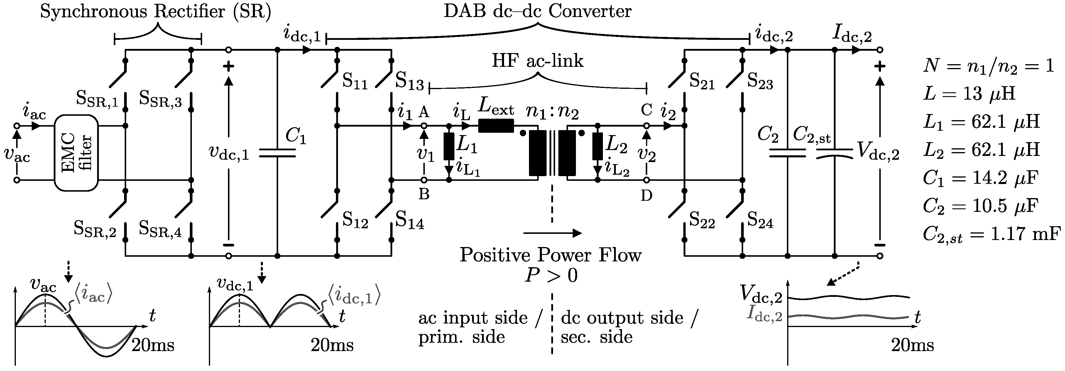
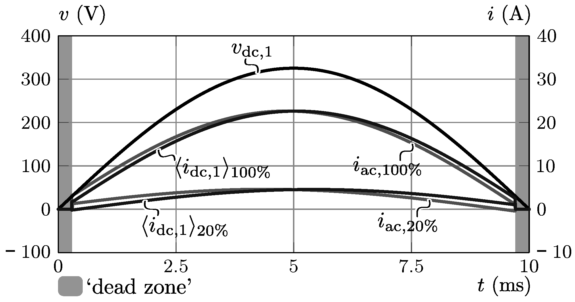
2. General Operating Principle of the 1-S Dual Active Bridge (DAB) AC-DC Converter
The investigated single-stage (1-S), single-phase ac-dc converter topology shown in Figure 1 consists of a synchronous rectifier (SR) and isolated full-bridge dual active bridge (DAB) dc-dc converter as the core building block, putting a small high-frequency (HF) filter capacitor in between. Also shown in Figure 1 are the principle current and voltage waveforms at the different converter ports. The SR switches at each zero-crossing of the ac line voltage , folding it into a dc voltage that varies according to the absolute value of , i.e., at twice the 50 Hz line frequency (), and that is directly fed to the input of the DAB dc-dc converter:
where is the amplitude of and . The DAB performs the PFC by actively shaping the switching-cycle averaged value of its input current in phase with :
where is the amplitude set-point of ac input current and the power flow direction in accordance with Figure 1:
Since the differential mode (DM) EMC input filter capacitance (see Section 4.4.1), which includes capacitor , draws a small reactive current from the grid, this current should be compensated in order to achieve unity power factor. This is done by controlling slightly lagging on , as can be seen in Figure 2 which depicts , , and within a 10 ms half period of the grid voltage for ac line current values of and (Note that around the zero crossing ( V V) the bridges of the DAB are inactive (‘dead zone’) as zero voltage switching (ZVS) power conversion is quasi impossible when the input voltage of the DAB is close to zero [25]). These currents respectively correspond to and of the nominal ac input power of . The exact control equation for , which compensates for , is given by Equation (2) of [25] and is not shown here for brevity of this paper. For the same reason, in the following only positive power flow operation () is discussed as, due to symmetry, the analysis and results for negative power flow are identical. It should be noted that the double line frequency (i.e., at ) component of the converter’s ac input power is directly transfered to the dc output side, which is due to the absence of a large intermediate dc-link energy storage element within this single-stage converter architecture. As discussed in Section 4.3.1, an electrolytic capacitor is placed at the dc output to (partly) filter this 100 Hz power component and prevent low-frequency (LF) stress on the load (e.g., battery).
Figure 2.
Ideal ac input-side quantities , , and within a 10 ms half period of the grid voltage for (100% power) and (20% power).
3. Optimal Zero Voltage Switching (ZVS) Operation of the DAB DC-DC converter
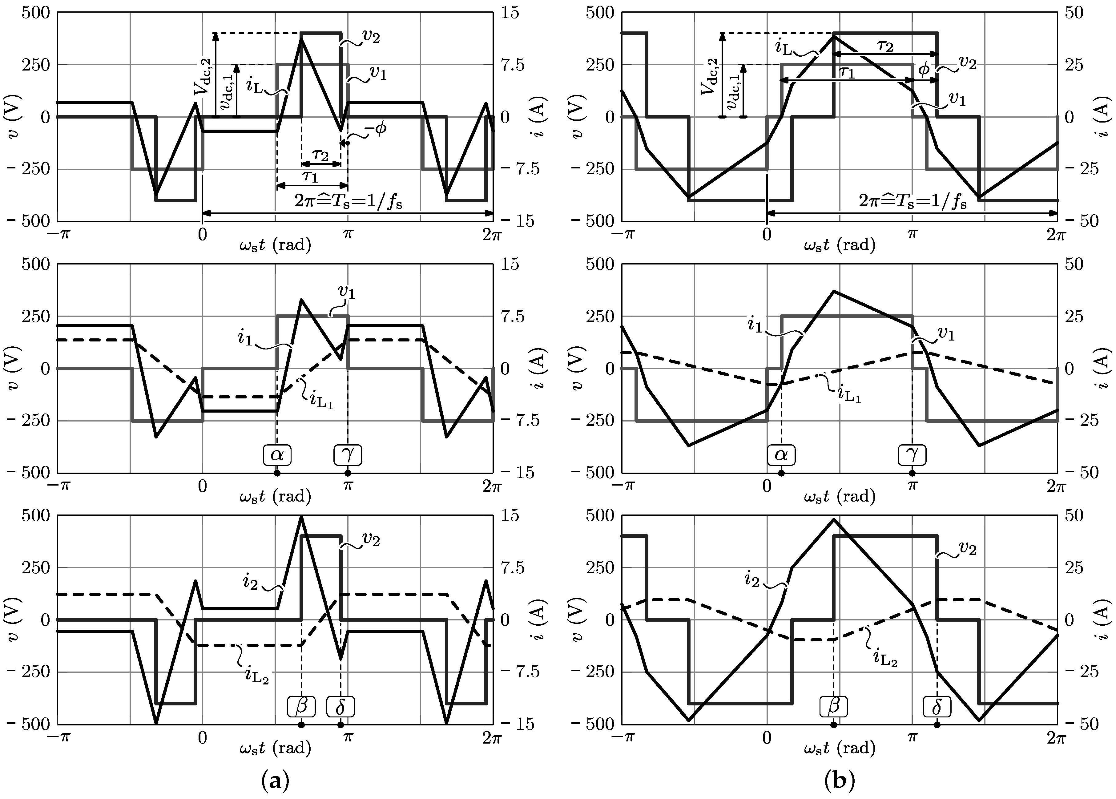
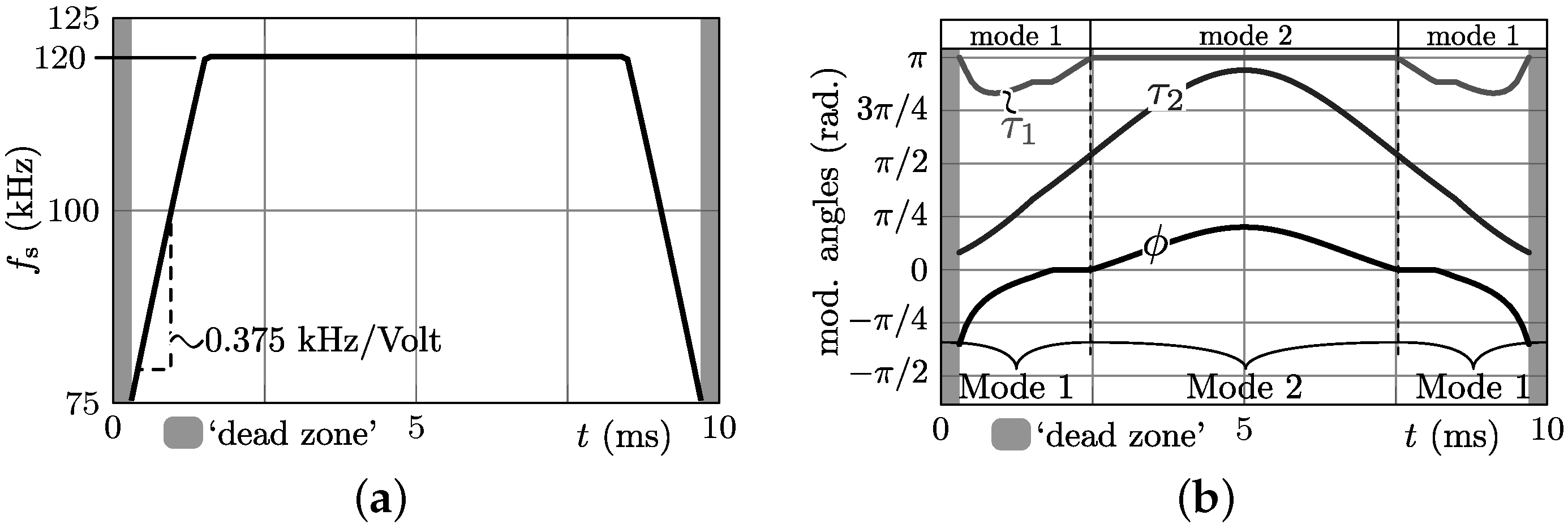
3.1. Operating Principle, Available Modulation Parameters, and Relevant Switching Modes
Control of the switching-cycle averaged DAB input current according to (2) can be done by proper modulation of the full bridges ( and ) of the DAB dc-dc converter [31] (see Figure 1). Thereby, the bridges produce phase-shifted edge-resonant square wave voltages and at the terminals of a HF ac-link. This link consists of a HF transformer (ratio ) and external series inductor . Also included in the ac-link are, so called, commutation inductances and which “inject” relatively small, purely reactive currents into the bridges of the DAB, enhancing the commutation of the bridge legs without contributing to the power flow. In [25,26] they have been shown to be essential elements for achieving full-operating-range ZVS of the DAB with smooth modulation parameter trajectories. On the assumption of ideal components, the DAB can be represented by the primary-side referred equivalent model shown in Figure 3, where the main energy transfer inductance consists of external inductance combined with the leakage inductances and (not shown in Figure 1) of the transformer:
Figure 3.
Simplified (lossless), primary-side referred equivalent model of the DAB dc-dc converter.
Figure 4, which depicts general waveforms of and for the two most appropriate switching modes, i.e., low-power mode 1 and high-power mode 2, for positive power flow of the DAB, defines the parameters available to modulate these voltages, being the phase-shift angle ϕ between and , the respective pulse-width modulation angles and , and the switching frequency . As in the following it is assumed that the switching frequency value/pattern is predefined (see Section 3.3), this results in a total of three “free” modulation parameters: . The respective inductor currents, induced by voltages and , are also shown in Figure 4, whereby:
and , induced in commutation inductances and , are the purely reactive currents that are “injected” into the bridges of the DAB. As a result, the bridge currents and are calculated as:
Figure 4.
Ideal high-frequency (HF) ac-link voltage/current waveforms for (a) Switching mode 1: low input current/power intervals and (b) Switching mode 2: high input current/power intervals, being derived using: V, V, and kHz. For mode 1 the selected modulation parameters are: rad., rad., rad., resulting in A. For mode 2 the selected modulation parameters are: , , , resulting in A.
Both active bridges of the DAB act as ac-dc converters towards their respective dc side, transforming bridge currents and into net dc currents and . Filter capacitors and bypass the HF components of and . The dc component of is thus the mentioned switching-cycle averaged DAB input current , which is calculated by averaging over one HF switching period , e.g. at a random instant :
Equations for , regarding the two switching modes of Figure 4, can be found in [25].
3.2. Efficient ZVS Modulation Scheme
The method used to calculate an efficient, full-operating-range ZVS modulation scheme for the DAB is presented in [25]. It is based on a constrained numerical optimization algorithm that calculated the modulation parameters in each DAB operating point {, , } based on a given switching frequency () and given circuit variables (see next section). Through this algorithm, in each DAB operating point the most appropriate switching mode, i.e., mode 1 or mode 2 of Figure 4, is automatically selected. The resulting modulation scheme leads to quasi-lossless ZVS operation at near-minimum RMS values of the HF bridge currents and and thus minimum conduction losses. Thereby, ZVS at all switching instants , β, γ, δ} of the DAB, which are defined in Figure 4, is ensured through incorporation of the charge () that is required to charge/discharge the MOSFETs’ non-linear parasitic output capacitances from 0 V to the corresponding dc-bus voltage (or vice versa) during commutation of the respective bridge legs. In Figure 4, switching instants α and β correspond with the positive rising edge of respectively and while γ and δ correspond with the respective positive falling edges. Consequently, the primary-side active bridge switches at , γ}, while the secondary-side active bridge switches at , δ}. () for the used MOSFETs is depicted in Figure 5b (The selection of the FAIRCHILD FCH76N60NF MOSFETs for the DAB is further detailed in Section 4.1.1), which is calculated using the characteristic of that is given in the data-sheet of the devices and shown in Figure 5a:
Figure 5.
(a) Characteristic of the non-linear parasitic output capacitance of the used FAIRCHILD FCH76N60NF MOSFETs ; (b) Charge required to charge/discharge the MOSFET’s non-linear parasitic output capacitance from 0 V to (or vice versa) during commutation of a bridge leg.
For the primary-side active bridge (index ‘p’) this charge is function of the DAB’s input voltage and is denoted (). For the secondary-side active bridge (index ‘s’) this charge is function of the DAB’s output voltage and is denoted ().
3.3. Selection of Circuit Variables
3.3.1. Switching Frequency ()
A nominal switching frequency of kHz is selected to accommodate a compact converter design without causing excessive switching frequency related losses. Moreover, thermal limitations apply at high switching frequencies, resulting in an increased total converter volume. The frequency of 120 kHz is chosen to stay well below these thermal limits. Furthermore, it has been been shown in [25] that at both ends of the 10 ms half mains period, where the DAB input voltage is low (see Figure 2), it is beneficial to linearly reduce . In these regions, ZVS is hard to achieve without making commutation inductances and very small, which would result in unacceptably high circulating currents and thus a low conversion efficiency. This has led to the following predefined switching frequency pattern (see also Figure 6a of Section 3.4):

Figure 6.
Resulting value trajectories of several quantities calculated for a half cycle of the nominal ac input voltage (, ) at the nominal ac input current of (positive power flow) and the nominal dc output voltage of V.
3.3.2. Transformer Turns Ratio
With regard to ZVS considerations, a good design rule is to determine the turns ratio of the HF transformer such that [25]. Given the DAB’s input and output voltage range, where V and V, this results in:
As can be seen from Equation (13), a wider output voltage range with V is feasible by selecting . However, it was an initial design choice to take , limiting to 370 V.
3.3.3. Main Energy Transfer Inductance
The maximum achievable DAB input current is obtained at and , mode 2, and is given by [25]. This maximum current needs to be higher than the peak value of the ac input current at maximum power, which equal to (= A). Therefore, the maximum allowable inductance value is determined by:
A good design guideline is to choose the value in the range [25], leaving sufficient margin for control purposes. This yields the final design value of H.
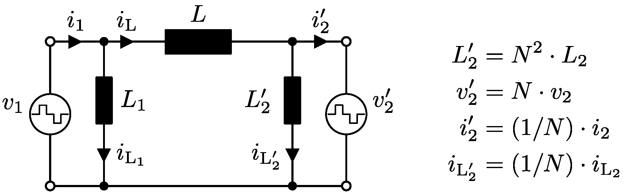
3.3.4. Commutation Inductances and
As mentioned in Section 3.3.1, there is a strong correlation between the lower value of (i.e., at low ) and the maximum allowed values of commutation inductances and . Determination of these values requires some iteration. Assuming = , the highest value for and that leads to full-operating-range ZVS, i.e., regarding the switching frequency pattern given by (12), has been found to be H, which is also the final design value.
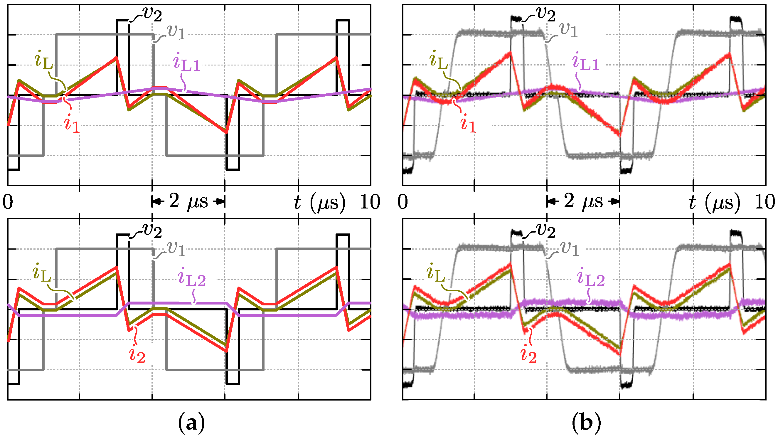
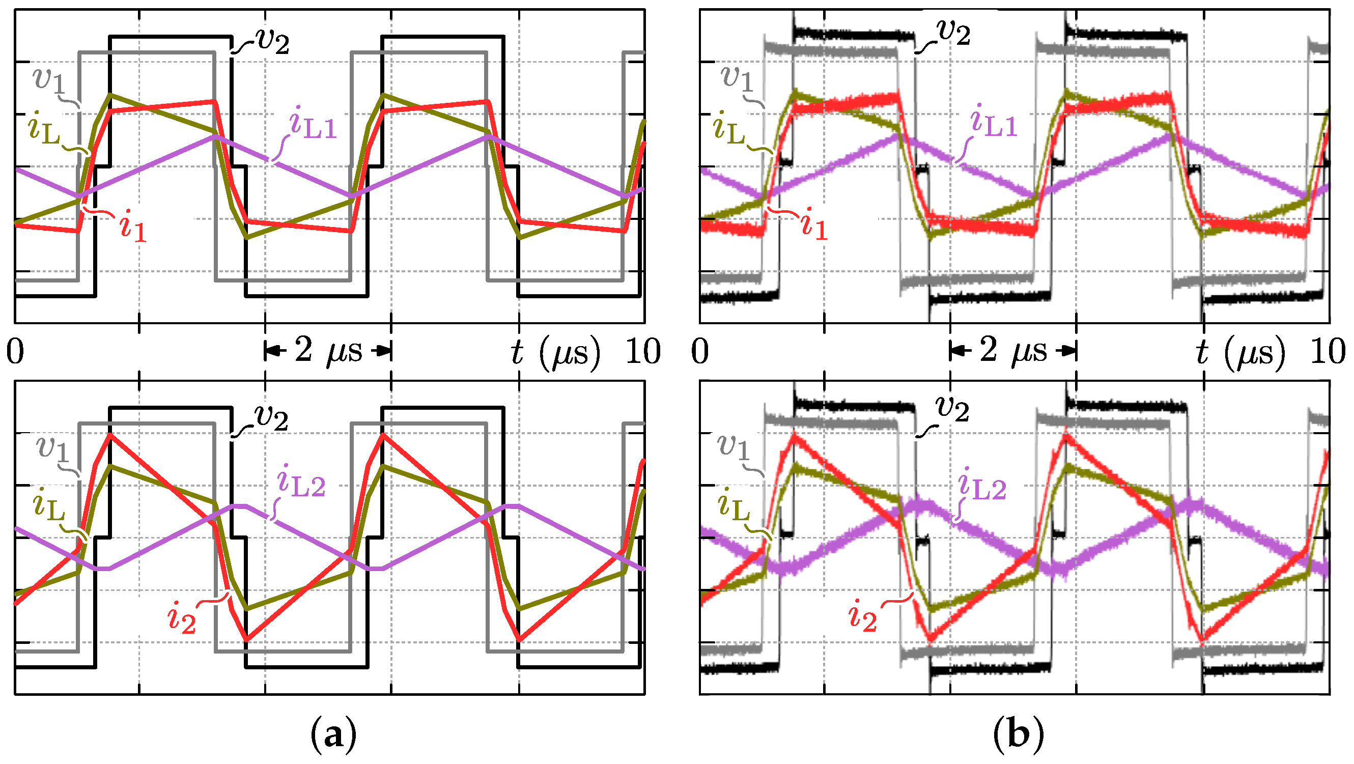
3.4. Simulation Results
Figure 6 illustrates the relevant simulation results that are obtained using the constrained numerical optimization algorithm presented in [25] for a run through a half-cycle (i.e., ms) of the nominal ac input voltage (, ) at the nominal ac input current of (positive power flow) and the nominal dc output voltage of V. Note that the values applied for correspond with line in Figure 2. The used circuit variables are derived in the previous section and are listed in the right inset of Figure 1 while the predefined switching frequency pattern () is given by (12) and shown in Figure 6a. The modulation parameters that result from the simulation are shown in Figure 6b, expectedly comprising only switching modes 1 and 2. From Figure 6c,d it can be seen that the available commutation charges and at the two most critical switching instants are higher than or equal to the minimum required commutation charges for achieving ZVS, i.e., respectively (primary-side active bridge) and (secondary-side active bridge). The same goes for the available commutation charges at the non-critical switching instants , γ} which are not shown for brevity. This means that ZVS of all the semiconductor devices is guaranteed in all operating points of the simulation run.
4. Modeling and Optimization of the Main Functional Elements
Based on the ZVS modulation scheme, the switching frequency pattern (), and circuit variables derived in Section 3, in this section the main functional elements of the 1-S DAB ac-dc converter are designed and optimized. Each sub-section is dedicated to the design of the individual elements, combining state-of-the art design methods/procedures, models for the component losses, and volume models with custom developed component-level optimization algorithms in order to obtain a high-efficiency and high-power-density converter design that is in compliance with the system requirements specified in Table 1.
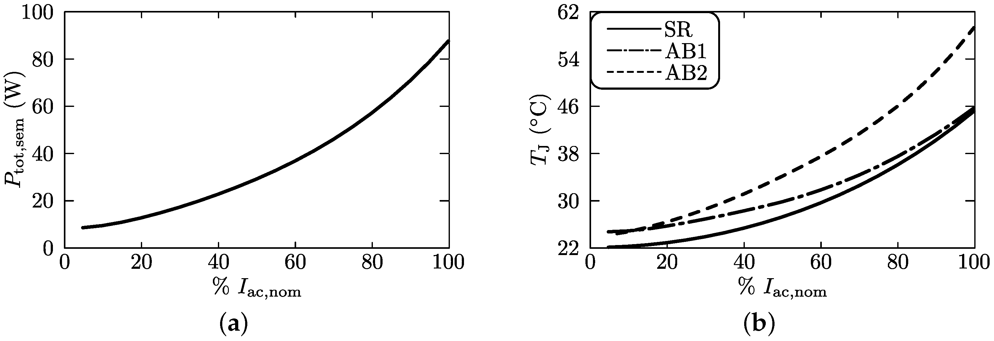
4.1. Semiconductors and Heat Sinks
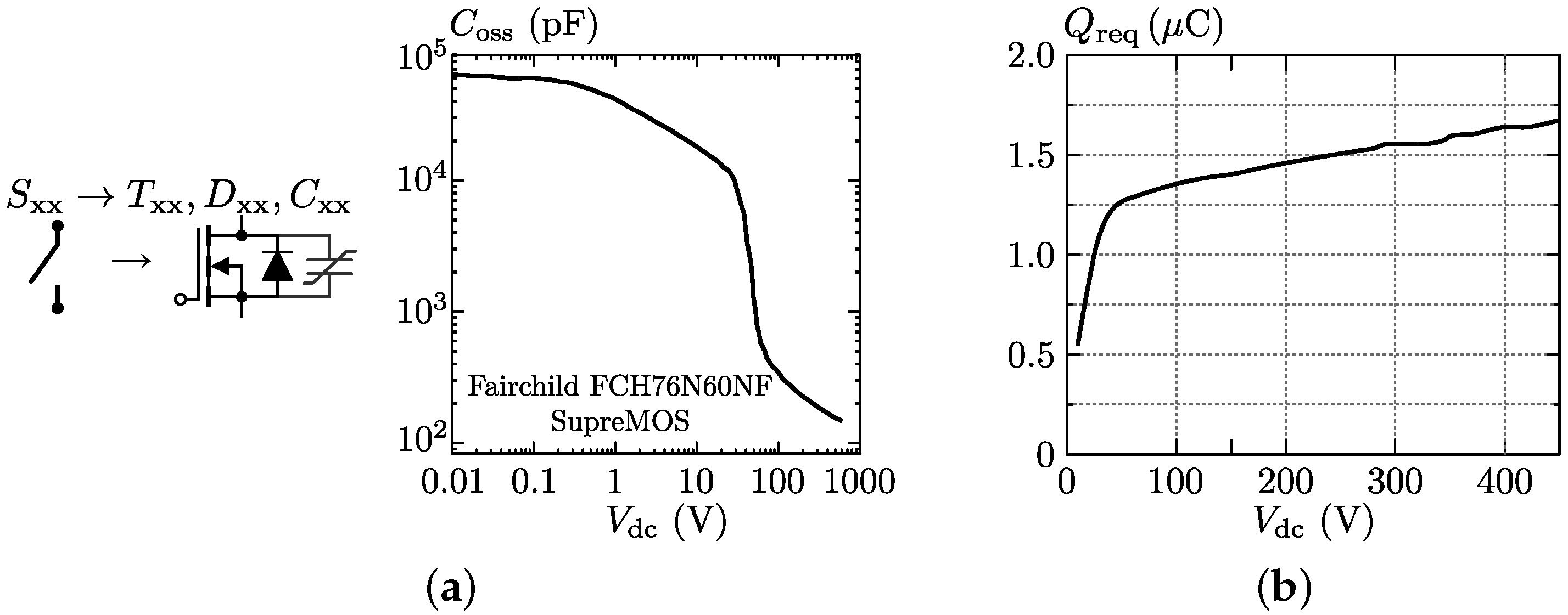
4.1.1. Semiconductor Selection
Each full-bridge of the DAB consists of four HF-switched MOSFETs, requiring characteristics that enable an excellent (soft-) switching performance and low conduction losses. The FCH76N60NF (FAIRCHILD) SupreMOS® high-voltage super-junction MOSFETs are selected, showing:
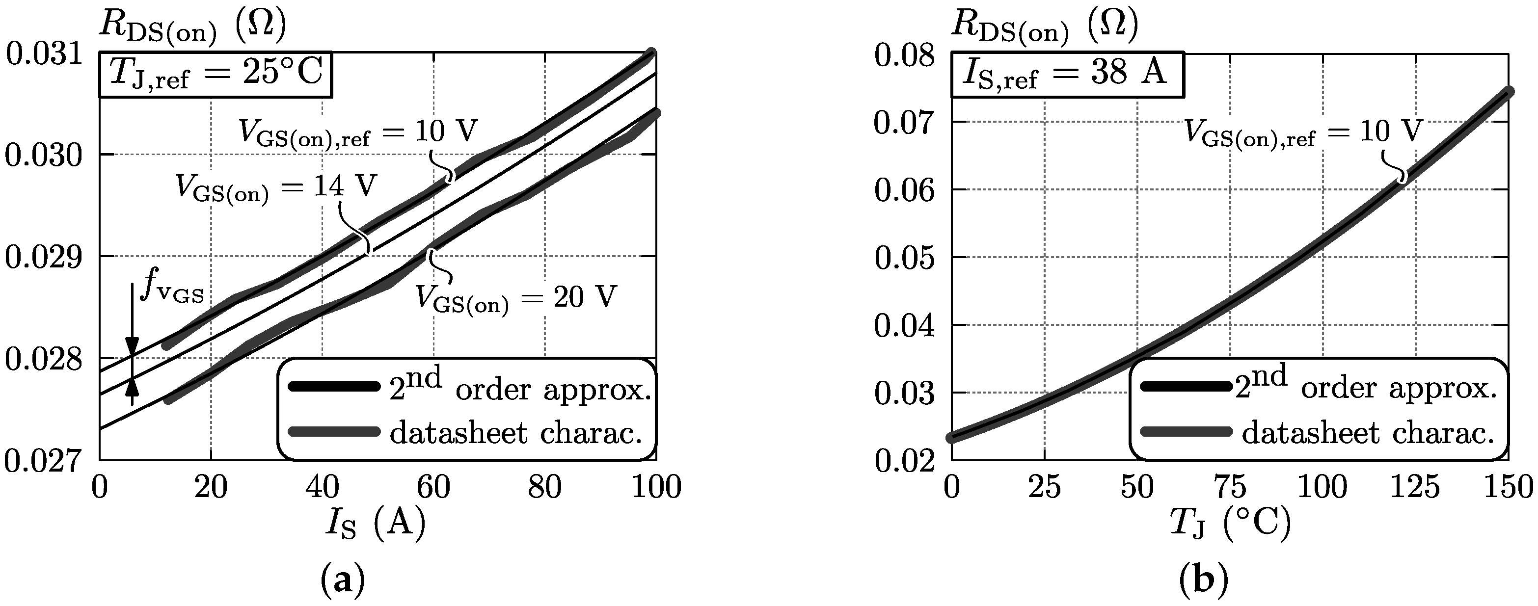
- A highly non-linear, not too big, parasitic output capacitance , enabling ZVS turn-off and turn-on. The characteristic of the FCH76N60NF MOSFETs is shown in Figure 5a;
- A low drain to source on-resistance and a low junction to case thermal resistance , being beneficial regarding the DAB’s conduction losses;
- A low total gate charge , leading to reduced turn-on and turn-off times, improved ZVS behavior (fast turn-off) [32], and reduced gate drive losses;
- An integrated fast body diode with low reverse recovery charge and low reverse recovery time , ensuring that all the energy will timely leave the transistor after a ZVS commutation.
Of main importance for the four LF-switched MOSFETs of the SR are the characteristics that enable a reduction of the SR’s conduction losses, being a low on-resistance and low junction to case thermal resistance . The switching-performance related characteristics are of less importance since the SR’s MOSFETs only change state two times per mains period. The STY112N65M5 (ST Microelectronics) MDmesh V power MOSFETs are chosen. Table A1 of Appendix A.1 lists the most relevant device parameters of both the FCH76N60NF and the STY112N65M5 MOSFETs.
4.1.2. Loss Models
Since the modulation scheme derived in Section 3.2 results in full-operating-range ZVS of the DAB, switching losses can be neglected in the analysis [10,28]. Therefore, only conduction losses and the losses of the gate drive units are considered. For the SR also the gate drive losses can be neglected as the MOSFETs of the SR are low-frequency switched (100 Hz).
Conduction losses: The conduction losses of a MOSFET are proportional to the drain to source on-resistance and to the squared RMS value of the conducted current (The conduction losses of the internal body diodes can be neglected as they only conduct current during a very small interval of the switching period ). Assuming a negligible junction temperature change within a full line cycle , the equivalent, line-cycle averaged conduction losses of a single MOSFET are determined by:
is the local, switching-cycle averaged RMS value of the current conducted by the switch under consideration, and is used in (16) to calculate the equivalent, line-cycle averaged RMS value . In steady-state, each switch of the DAB conducts during half a switching cycle /2. As a result, for the switches of both active bridges are determined by:
and are the switching-cycle averaged RMS values of bridge currents and . Each SR switch conducts during half a mains period . Assuming that the HF components of the DAB input current are bypassed by HF filter capacitance , for each SR switch can be approximated as:
To calculate the resulting conduction losses using (15)–(19), the dependency of the MOSFET’s on-resistance on the junction temperature and on the switch current has to be modeled. Figure 7 depicts these dependencies for the FCH76N60NF MOSFETs. The datasheet characteristics (gray lines) can be described by a second order approximation (Similarly, a second order approximation can be used to describe the characteristics of the SR’s STY112N65M5 MOSFETs.) (black lines) according to:
where the equivalent, line-cycle averaged RMS values for the switches of active bridge 1, active bridge 2, and the SR are respectively given by (17)–(19). is the equivalent, line-cycle averaged junction temperature of the switch under consideration:
which is calculated using the thermal network model that will be presented in Section 4.1.3. The coefficients (, , and , , ) required to evaluate (20) and (21) for both used MOSFET types are given in Table A2 of Appendix A.1 where , , and are the datasheet reference values. By combining (20) and (21), a generalized equation can be found which expresses as a function of the deviations () and () of respectively the junction temperature and the switch current from the reference values and :
Figure 7.
Dependency of the on-resistance on (a) the switch current and (b) the junction temperature , regarding the FAIRCHILD FCH76N60NF MOSFETs.
is the reference datasheet value as listed in Table A1. The coefficients (, and , ) for both used MOSFETs are given in Table A3. In (23) a displacement term , determined using linear interpolation (see Figure 7a), is introduced in order to take into account the dependency of on the turn-on gate voltage . For the FCH76N60NF MOSFET, and regarding the applied turn-on gate voltage of V, was found to be . For the STY112N65M5, could not be calculated due to the absence of information in the datasheet about the gate voltage dependency of , and is assumed to be zero. This leads to a negligible overestimation of the SR’s conduction losses.
Gate drive losses: Assuming an efficiency of 90% for the gate drive units (), the equivalent, line-cycle averaged gate drive losses are:
since the SR’s gate drive losses can be neglected. is the gate to source voltage swing which is 18 V ( V) for the custom designed gate drive circuits. is the total (typical) gate charge, measured for the reference gate voltage swing given in Table A1 of Appendix A.1.
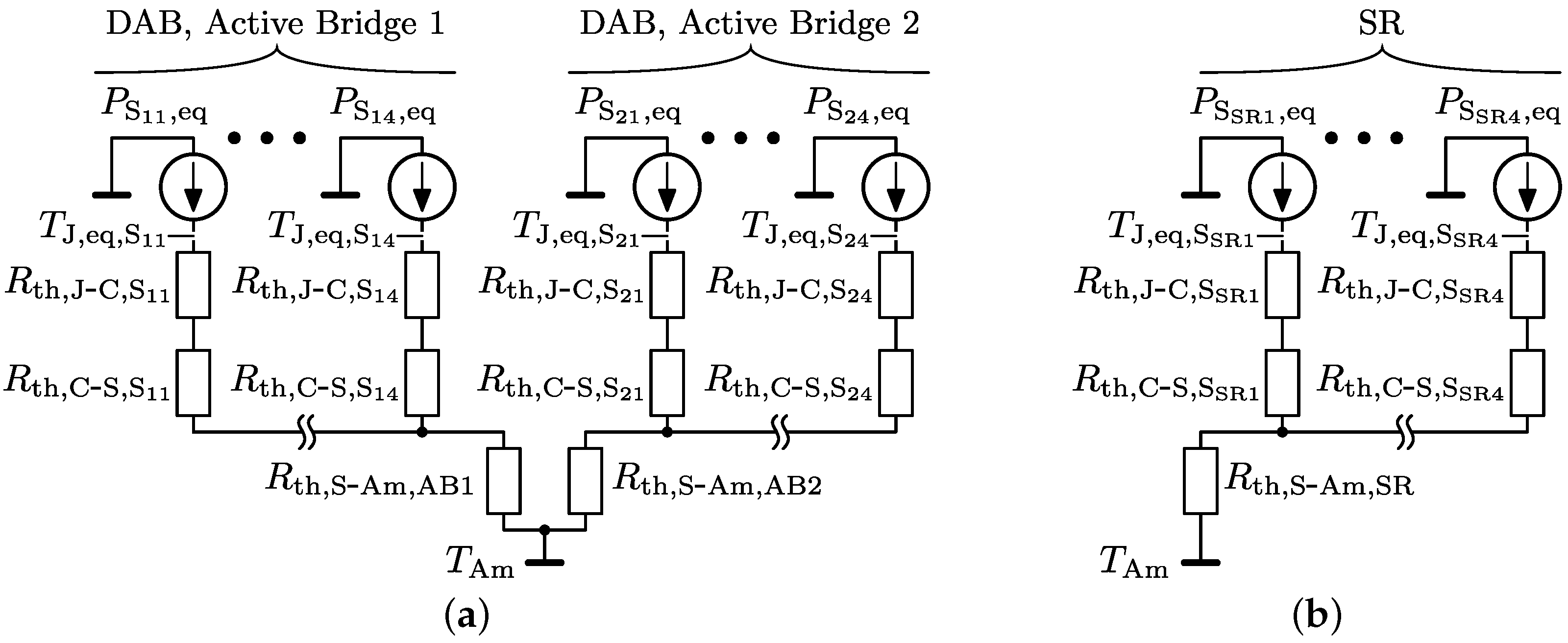
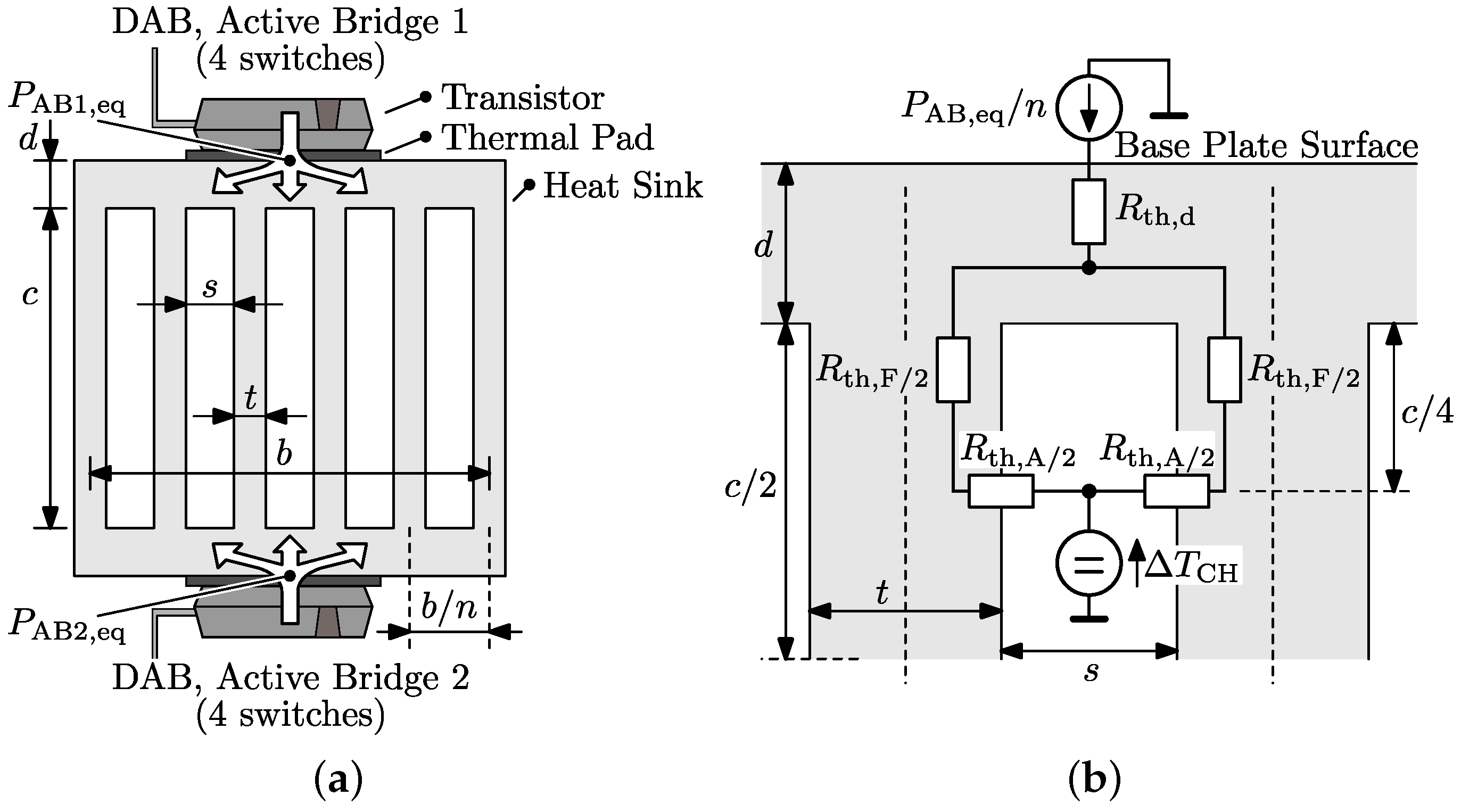
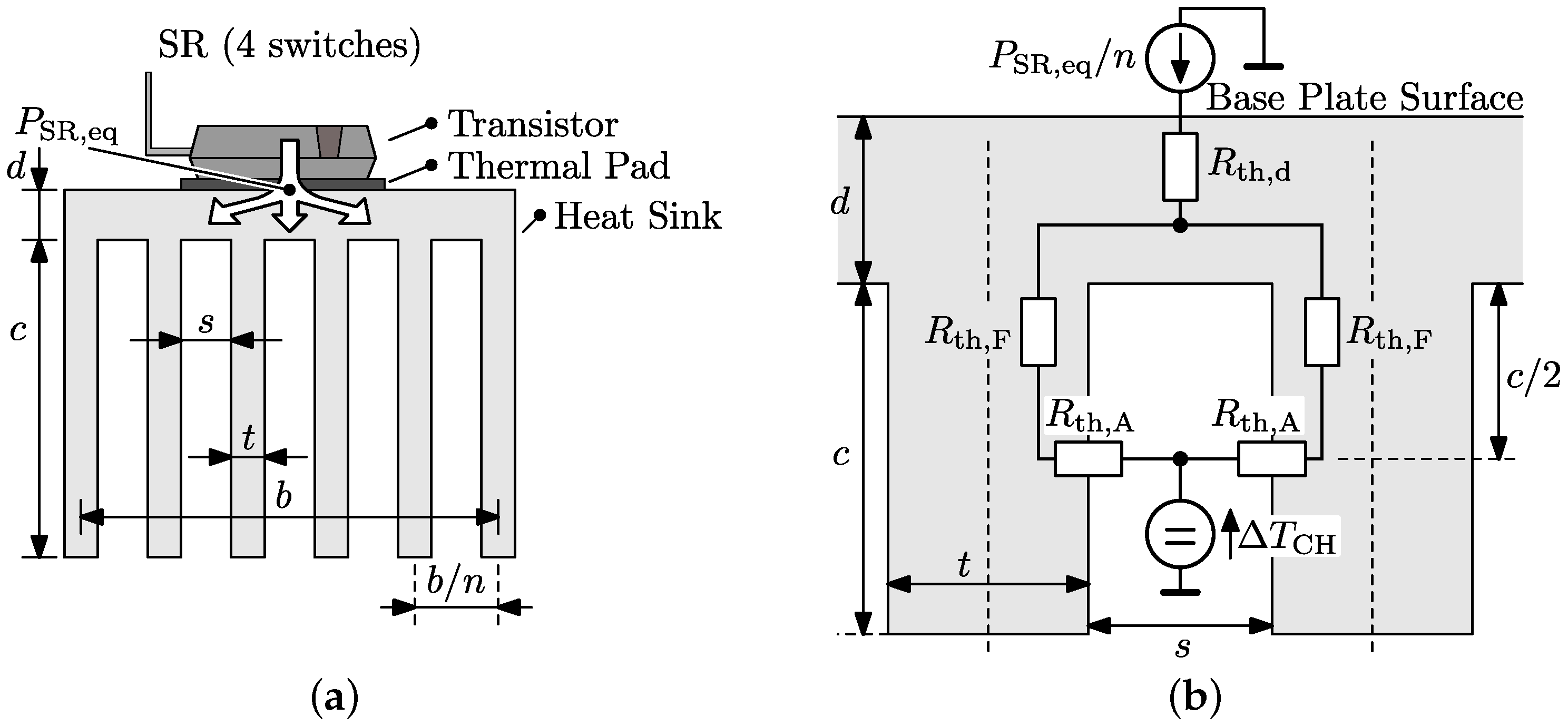
4.1.3. Heat Sink Assembly and Thermal Network Model
Autonomous air cooling by means of forced convection is one of the system requirements defined in Table 1. Thereby the heat generated by the power devices is subtracted via a finned heat sink in combination with a fan. For the two active bridges of the DAB, a heat sink geometry with dual-sided base plate, as shown in Figure 8a, is considered. The four switches of the primary-side active bridge (active bridge 1; AB1) are mounted on the top-side base plate while the four switches of the secondary-side active bridge (active bridge 2; AB2) are mounted on the bottom-side base plate. The four switches of the SR are mounted on a heat sink geometry with single-sided base plate, as shown in Figure 8b. The resulting stationary heat transfer models are depicted in Figure 9, where:
- are the junction to case thermal resistances of the switches;
- are the thermal resistances of the thermal pads (the Hi-Flow 300P thermal pads from Bergquist are used for all switches).;
- and (=) are the total thermal resistances between the surface of the heat sink (i.e., seen from one base plate) to the ambient, for the heat sink of the DAB;
- is the total thermal resistance between the surface of the heat sink (i.e., the surface of the base plate) to the ambient, for the heat sink of the SR.
Figure 8.
Heat sink-semiconductor assemblies for (a) the DAB and (b) the synchronous rectifier (SR).
Figure 9.
Stationary heat transfer model of the heat sink assembly of (a) the DAB and (b) the SR.
for the used MOSFETs are given in Table A1 of Appendix A.1, while for all switches is defined by where is the thickness ( m), the thermal conductivity ( W/mK), and the cross section area of the thermal pads ( m for the FCH76N60NF MOSFETs and m for the STY112N65M5 MOSFETs). (=) and are obtained from the heat sink optimizations performed in Section 4.1.4. Referring to Figure 9, the equivalent junction temperature of a switch can now be expressed as:
where, under the assumption that half the gate drive losses of a switch are internally dissipated in the switch while the other half is dissipated externally (i.e., in the gate drive units and gate resistors),
and are respectively calculated with (15), (24) and (25). is the ambient temperature. At this point all the information required to calculate the equivalent, line-cycle averaged semiconductor losses is available. Due to the interdependency of the quantities, a numerical solver is applied to solve: , , and .
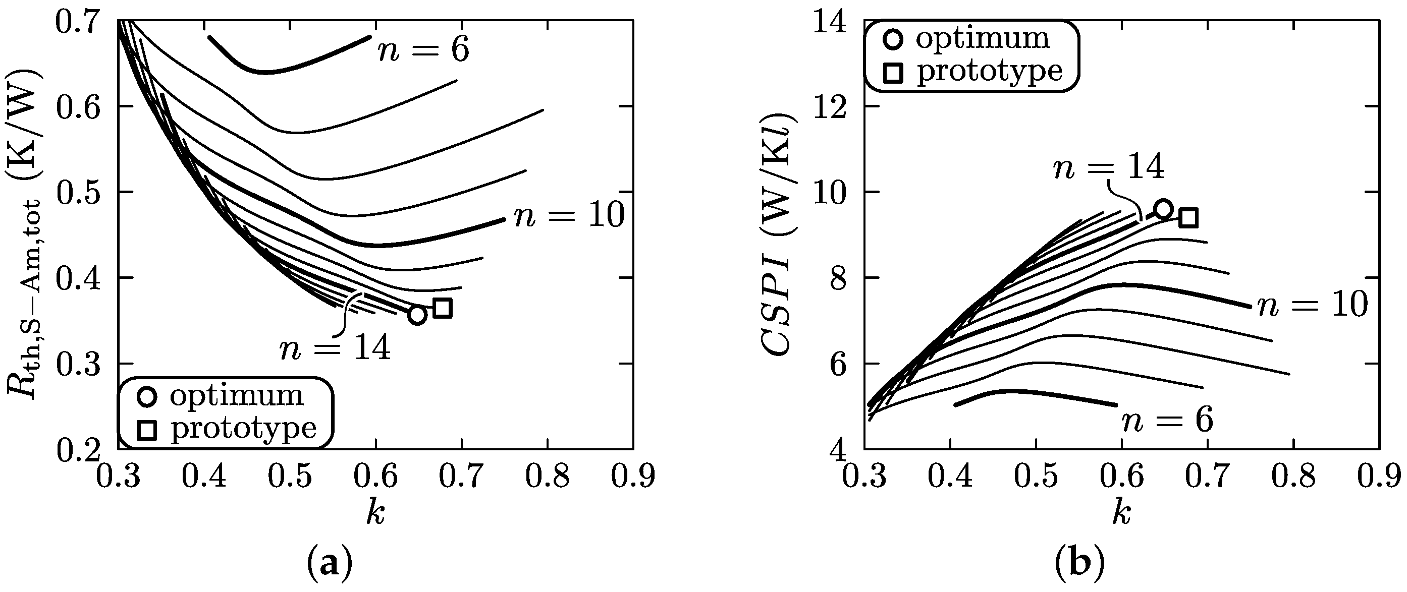
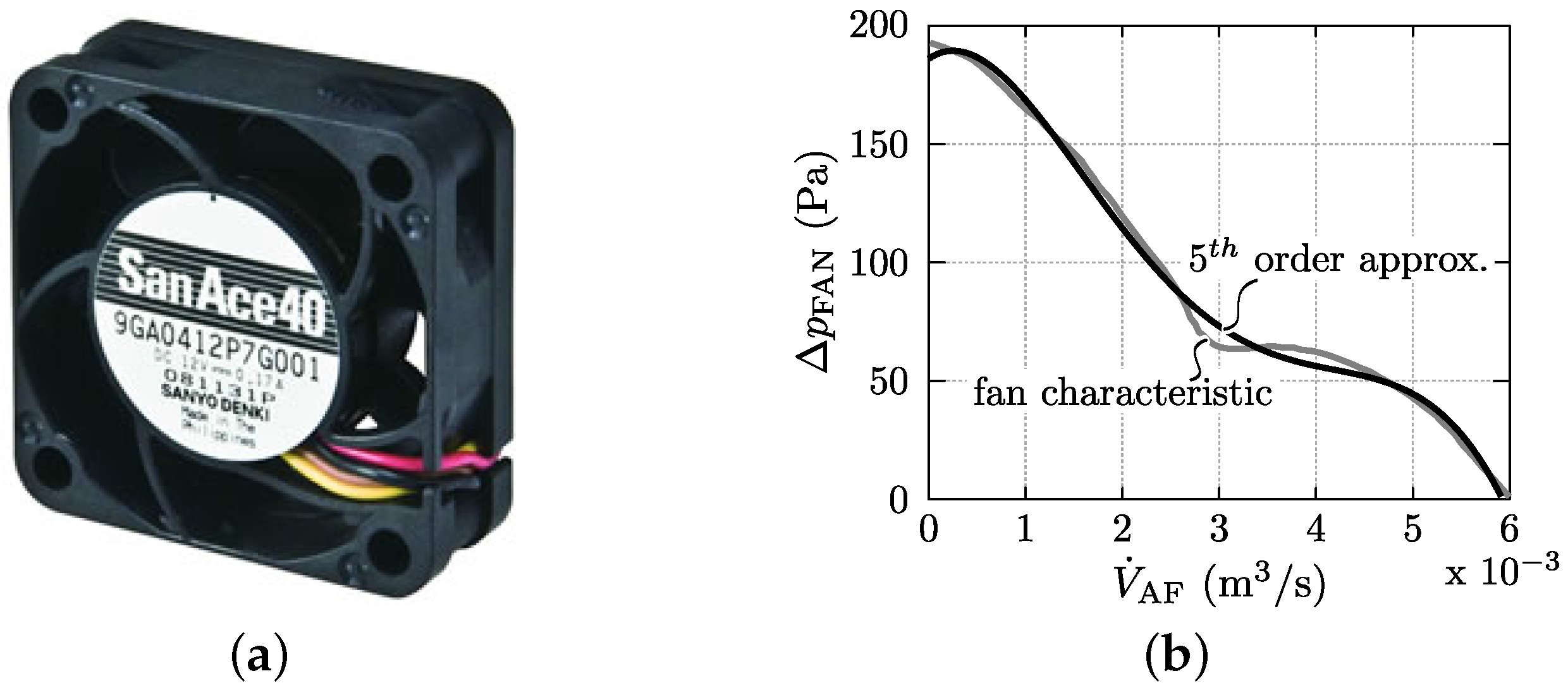
4.1.4. Heat Sink Optimization
The surface-to-ambient thermal resistances (=) and of the forced-convection-cooled heat sinks are obtained from optimizations in which the heat sink geometries are determined in a way that, for a given fan and for given outer heat sink dimensions, these thermal resistances are minimized. This involves calculation of the thermal resistance for conductive heat transfer through the heat sink material, the thermal resistance for convective heat transfer, and the temperature increase of the air flowing through the heat sink channels. The applied optimization procedure and thermal models are described in detail in [33,34], and are summarized in the following, only considering stationary heat transfer. The involved variables are given in Table 2 (, , , and are slightly temperature dependent. In order to simplify the analysis, the values at an average channel air temperature of = 80 C are used).
Table 2.
Variables used for the calculation of the thermal resistance of a finned heat sink with fan, and for the calculation of the air flow rate in, and the pressure drop across the air channels of the heat sink.
For the heat sink geometry with dual-sided base plate shown in Figure 8a, the conductive and convective heat transfer are modeled according to Figure 10. The thermal resistance from the base plate surface (index ‘S’) of this heat sink to the ambient (index ‘Am’), i.e., the air temperature at the heat sink inlet, is described by:
with:
Figure 10.
(a) Heat sink geometry with dual-sided base plate, considered to cool the switches of the DAB’s active bridges; (b) Thermal network describing stationary heat transfer between the surface of a base plate and the air in the heat sink channel (temperature ).
For the heat sink geometry with single-sided base plate shown in Figure 8b, the conductive and convective heat transfer are modeled according to Figure 11. is now described by:
with:
Figure 11.
(a) Heat sink geometry with single-sided base plate, considered to cool the switches of the SR; (b) Thermal network describing stationary heat transfer between the surface of the base plate and the air in the heat sink channel (temperature ).
The last term of the thermal resistance in both (28) and (32) considers the average temperature rise of the air from channel inlet to channel outlet. Calculation of the convective heat transfer coefficient h and the total volume flow of the air in the heat sink channels, which are both required for the calculation of in (28) and (32), goes as follows.
Based on (53)–(56) of Appendix A.1, the air flow pressure drop in the heat sink channels for laminar (‘lam’) and turbulent (‘turb’) flow can be calculated. Balancing the pressure drop with the pressure of the fan, as defined by the fan characteristic in (57), gives the fan’s operating point which defines the air flow and pressure drop in the heat sink channels. Using (58), the Reynolds number is found as well. In case of laminar flow, with Re < 2300, Equation (59) is used to calculate the Nusselt number, which describes the convective heat transfer from the channel walls into the air. In case of turbulent flow, with Re > 2300, the Nusselt number is calculated with Equation (60). Using (61), the convective heat transfer coefficient h of the configuration is finally found.
By repeating the above procedure for different heat sink geometries, an optimal set of geometrical parameters (d, t, b, c, s, L, and n) can be found which leads to the lowest thermal resistance . This is done for both heat sinks, assuming predefined outer heat sink dimensions (i.e., variables b, c, L, and d). As a result, the geometric parameters that are varied during the optimization are the number of channels n and the fin spacing ratio k, which is equivalent to varying the channel width s; see Equation (54). The results are discussed below.
Heat sink of the DAB with dual-sided base plate, conform Figure 10: The fan size defines the heat sink front geometry as only the fins that are facing the fan contribute to the convective heat transfer. After thorough iteration of the mechanical design of the final prototype converter, a 40 mm × 40 mm fan turned out to be most feasible, leading to the selection of the SanAce40GA shown in Figure 12 (The SanAce40GA fan type 9GA0412P7G001, see Figure 12a, has been selected due to its high static pressure, high air flow rate, and low sound pressure level, in combination with an ultra low power consumption). Consequently, a heat sink geometry with mm is most appropriate in order to fully utilize the fan. The pressure-flow curve, (), of this fan is depicted in Figure 12b (gray line) and can be described by a 5th order approximation (black line in Figure 12b):
Figure 12.
(a) Picture of the selected fan: SanAce40GA, type 9GA0412P7G001, 40 mm × 40 mm × 15 mm, 12 V; (b) Datasheet pressure-flow curve (gray line) and 5th order approximation (black line).
The length L of the heat sink channels must be large enough so that sufficient space is provided on the base plates to mount the switches. Assuming a minimum spacing of 5 mm between the packages of adjacent switches, a minimum spacing of 10 mm between the base plate borders and a package, and a package width of approximately 16 mm for the TO-247 package, the minimum base plate length becomes mm. Preferably the maximum base plate length should not be much higher than , assuring homogeneous heat distribution across the base plate. The final base plate length is mm. The base plate thickness d should be large enough to homogeneously spread the heat and small enough to limit the thermal resistance of the heat sink. The value mm is selected as a good trade-off between these two considerations.
Figure 13 shows the results of the optimization, applying the assumed outer heat sink dimensions, i.e., the above discussed variables b, c, L, and d, and assuming a minimum achievable fin thickness and channel width of 1 mm, which are enabled by using high-end milling machines. Furthermore, aluminium is considered for the heat sink material, defining the thermal conductivity value W/mK. Figure 13a depicts the relation between (=) and the two geometric parameters n and k that are independently varied (The multiplication of with a factor “0.5” is required since is experienced from just one base plate of the heat sink and thus has to be divided by two in order to take both base plates (top and bottom) into account). The performance indices and parameter values for the resulting (optimal) heat sink design are given in the top inset of Table A4 of Appendix A.1. There, is the boxed volume of the heat sink, excluding the fan and an additional airflow inlet between the fan and the heat sink. is the volume of the cooling system, including the heat sink, the fan, and an additional airflow inlet between the fan and the heat sink. is the cooling system performance index [33,34,35], which is an objective measure that allows to compare different cooling system designs with regard to power density. For the cooling system of the DAB, with dual-sided base plate, is defined as [34]:
Figure 13.
Optimization result for the heat sink of the DAB (geometry with dual-sided base plate, cf. Figure 10), assuming a minimum achievable fin thickness and channel width of 1 mm: (a) Total surface-to-ambient thermal resistance (=0.5 ×) as function of n and k, which are independently varied; (b) Cooling system performance index as function of n and k.
If a heat sink design shows a that is two times higher than the of another one, the cooling volume can be made two times smaller for the same thermal resistance. Knowing that typical commercially available heat sink/fan combinations have a of around 5, the extensive heat sink optimization, achieving , is justified. The (boxed) volume , which besides the heat sink, the fan, and the airflow inlet also includes the semiconductor switching devices, is also listed in Table A4. The bottom inset of Table A4 shows the performance indices and design parameters of the heat sink used in the final (prototype) converter, and considered for further calculations. It in fact is a near-optimal design, which is due to the fact that the minimum achievable fin thickness and channel width were restricted due to limitations of the in-house manufacturing machines/tools.
Heat sink of the SR with single-sided base plate, conform Figure 11: For the heat sink of the SR, once more the 40 × 40 mm SanAce40GA fan (see Figure 12) is selected. As the SR requires less cooling effort than the DAB, the heat sink’s front geometry values are reduced from mm (most appropriate in order to fully utilize the fan) to mm and mm. This allows to use part of the fan’s airflow to cool other electronic components. The reduced airflow in the heat sink channels due to the area reduction of the heat sink’s front geometry is taken into account by multiplying with the heat-sink-front-area to fan-area ratio . Furthermore, a slightly increased channel length of mm is used and a base plate thickness of mm is applied. Once more, a minimum achievable fin thickness and channel width of 1 mm are assumed.
The performance indices and parameter values for the resulting (optimal) heat sink design are given in the top inset of Table A5 of Appendix A.1. The bottom table inset shows the values for the heat sink design of the final (prototype) converter. For the reason mentioned above this is a near-optimal design and is considered for further calculations. Note that the part of the fan that does not faces fins is not included in the calculation of , and that for the heat sink with single-sided base plate is defined as [34]:
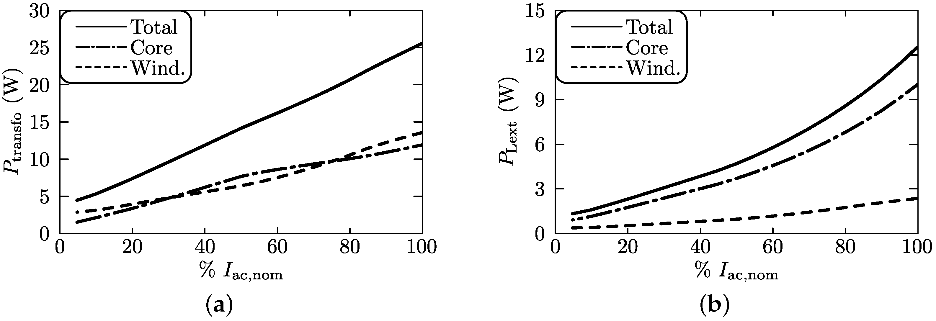
4.2. Magnetic Elements of the DAB: Inductors and Transformer
As mentioned before, the DAB dc-dc converter consists of three discrete magnetic elements: the HF ac-link transformer, the external series inductor , and the primary-side commutation inductor . The secondary-side commutation inductance is implemented by the magnetizing inductance of the transformer (), avoiding increased volume and costs. Referring to the equivalent DAB model shown in Figure 3, the main energy transfer inductance is calculated with Equation (4), where and are the primary- and secondary-side leakage inductances of the transformer. Consequently, to determine the inductance value , the transformer needs to be designed first (i.e., and result from the final transformer design). Remind that the values of , , , and (=) are derived in Section 3.3 and are given in the right inset of Figure 1.
4.2.1. Design and Optimization Procedure
Two optimization algorithms, i.e., for the transformer and for the inductors, are developed in order to optimize each magnetic element with regard to the losses and their (boxed) volume. Apart from the currents and voltages, losses in inductors and transformers depend on the geometry and the arrangement of the windings, the type of wires, the type of the core, and the geometry and material of the core. The resulting volume is mainly determined by the core geometry and the end turns of the windings. For the different optimizations, planar cores are considered because of their excellent electromagnetic and thermal characteristics and their advantageous properties with respect to the achievable power density [36,37]. All possible EELP and EILP core combinations from FERROXCUBE (ferrite core material: 3F3 and 3F4) and EPCOS (ferrite core material: N49, N87, N92, and N97) in the dimensions range from ELP32 up to ELP64 are considered. The number of stacked cores is limited by setting a maximum of 15 cm to the total core length. Litz wires are chosen to reduce eddy current losses in the windings [38,39,40], being particularly effective at high switching frequencies. Furthermore, four possible winding arrangements are investigated, including split, concentric, hexagonal and orthogonal type windings. Also the paralleling of several Litz bundles, as well as the interleaving (for the transformer) of the windings, is implemented in the algorithms.
All possible combinations of above mentioned design variables are top level iterated. For each iteration, in a first step, the reluctance model of the considered magnetic element is calculated according to the methods proposed in [41], which inter alia provides a new analytical approach in order to determine the 3D air gap reluctance . The inductance values, i.e., , , and (=), are controlled with the air gap length (constrained to mm), while guaranteeing that the peak flux density does not exceed a predefined maximum value . This introduces an upper and a lower limit to the possible number of turns. For the transformer, the minimum and maximum number of turns, i.e., respectively , for the primary-side winding are determined by:
where is the maximum primary-side referred Volt-seconds product, the effective core cross section, the core reluctance, the air gap reluctance, and (=) the primary-side referred magnetizing inductance. The number of turns for the primary-side winding of the transformer then needs to be in the range . Evidently, the number of turns for the secondary-side winding is directly linked to via the transformer’s turns ratio . For the inductors, the minimum and maximum number of turns, i.e., respectively , are determined by:
where is the peak inductor current and (= or ) the inductance value of the considered inductor. The number of turns for the inductors then needs to be in the range . The upper boundary of the maximum allowed flux density is set by the core material saturation flux density at a core temperature of C, applying a 30% safety margin. Subsequently, using an inner iteration loop, the number of turns (transformer) is varied from to while the number of turns (inductors) is varied from to .
In a second step, a predefined objective function, which is determined by the sum of the core losses and the winding losses of the magnetic element at nominal operating conditions of the DAB, is minimized for each of above iterations. The applied loss models are summarized in Section 4.2.2. The optimization algorithm used to minimize the cost function iterates the number of strands in the Litz bundles, as well as the diameter of the individual strands, in order to achieve a window filling that is optimal with regard to the winding losses. Thereby, constraint functions set restrictions on the positioning of the individual Litz bundles by bringing into relation the number of strands, the strand diameter, and wire positioning functions with the given core window area, taking into account creepage distances.
4.2.2. Loss Models
In this section, the models used to calculate the winding and core losses of the magnetic elements are summarized. For the calculation of the core losses, the improved Generalized Steinmetz Equation (iGSE) [40,42] has been evaluated as the most accurate model which only requires the Steinmetz material parameters. This method takes into account the losses due to domain wall motion, which is directly related to the time dependency of the core’s flux density. Therefore the iGSE is applicable for non-sinusoidal flux waveforms such is the case for the magnetic components of the DAB, which experience piecewise-linear flux-time functions. With the iGSE, the per-unit-volume (index ‘V’) core losses are calculated using the Steinmetz parameters k, α, and β, according to:
with:
where is the peak-to-peak flux density. The Steinmetz parameters k, α, and β are extracted out of the core’s data sheets, providing information about the per-volume-unit core losses as a function of frequency f, peak flux density , and temperature T. This enables extraction of k, α, and β using the empirical Steinmetz Equation , which is valid for sinusoidal excitation only.
Regarding winding losses, the ohmic losses in the Litz wires (further referred to as Litz bundles) can be separated into skin effect losses from self-induced eddy currents inside the conductors, external proximity effect losses from eddy currents due to the external magnetic field that originates in the air gap fringing field and in the magnetic field from neighboring Litz bundles, and internal proximity effect losses from eddy currents due to the internal magnetic field that is produced by the bundle itself. The per-unit-length (index ‘L’) skin-effect losses (including the dc losses) of a Litz bundle consisting of strands, are calculated with [40]:
where are the Fourier amplitude coefficients of the total current in the Litz-wire bundle at the different harmonic frequencies f. is the per-unit-length dc resistance of a single strand: , with the diameter of the strand and σ the electric conductivity of the conductor material ( 1/Ωm for the considered Litz wires). is the skin-effect factor:
with , where δ is the skin depth according to . is the permeability of the conductor material ( H/m for air and copper). The per-unit-length proximity losses in a Litz bundle are calculated as [40]:
is the diameter of the Litz bundle while is the proximity-effect factor:
is the external magnetic field that originates in the air gap fringing field and in neighboring Litz bundles, and is calculated using the 2D analytical approach proposed in [40]. This approach relies on an imaging and mirroring method in order to inter alia model the impact of a surrounding magnetic conducting material. Thereby the air gap fringing fields are modeled by means of fictitious conductors with eddy currents equal to the magneto-motive force across the air gap. , with ; see last term of (47), is the internal magnetic field across one strand, which originates in its neighboring strands. For the calculation of it is assumed that the current is equally distributed over the Litz bundle’s cross-sectional area.
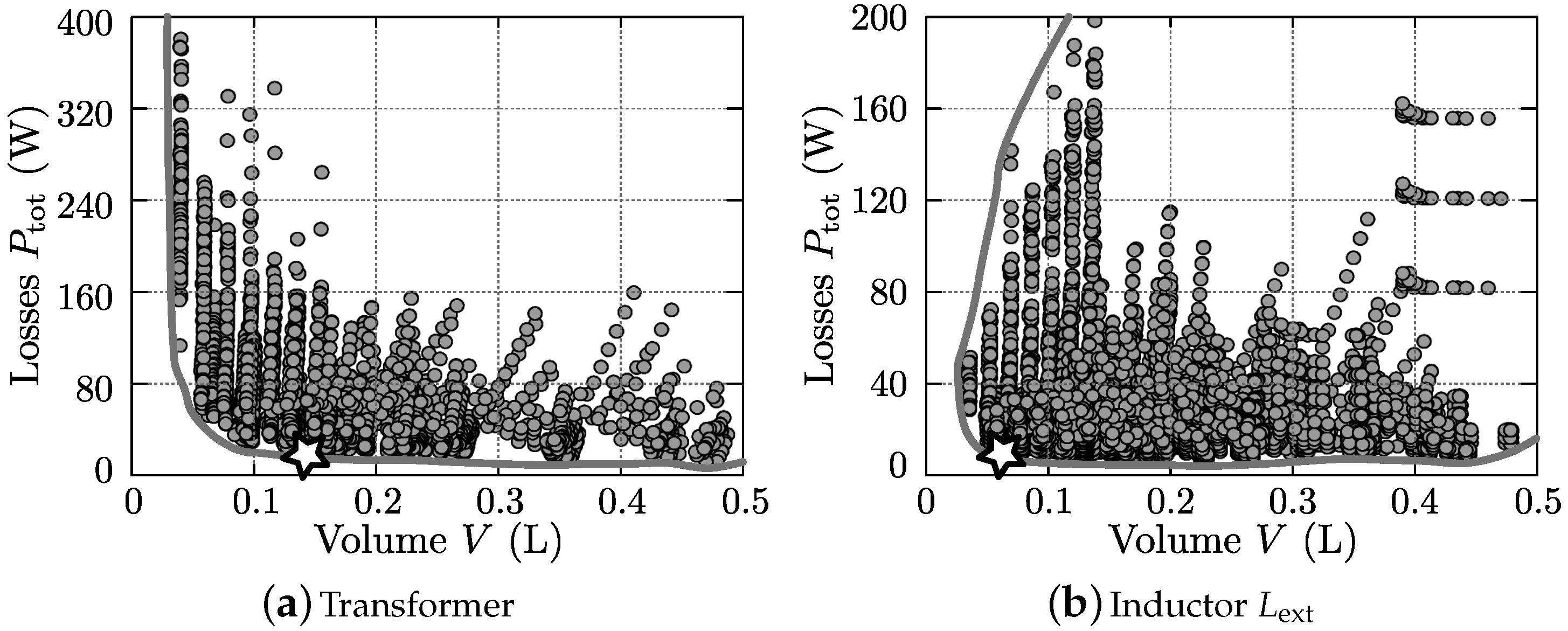
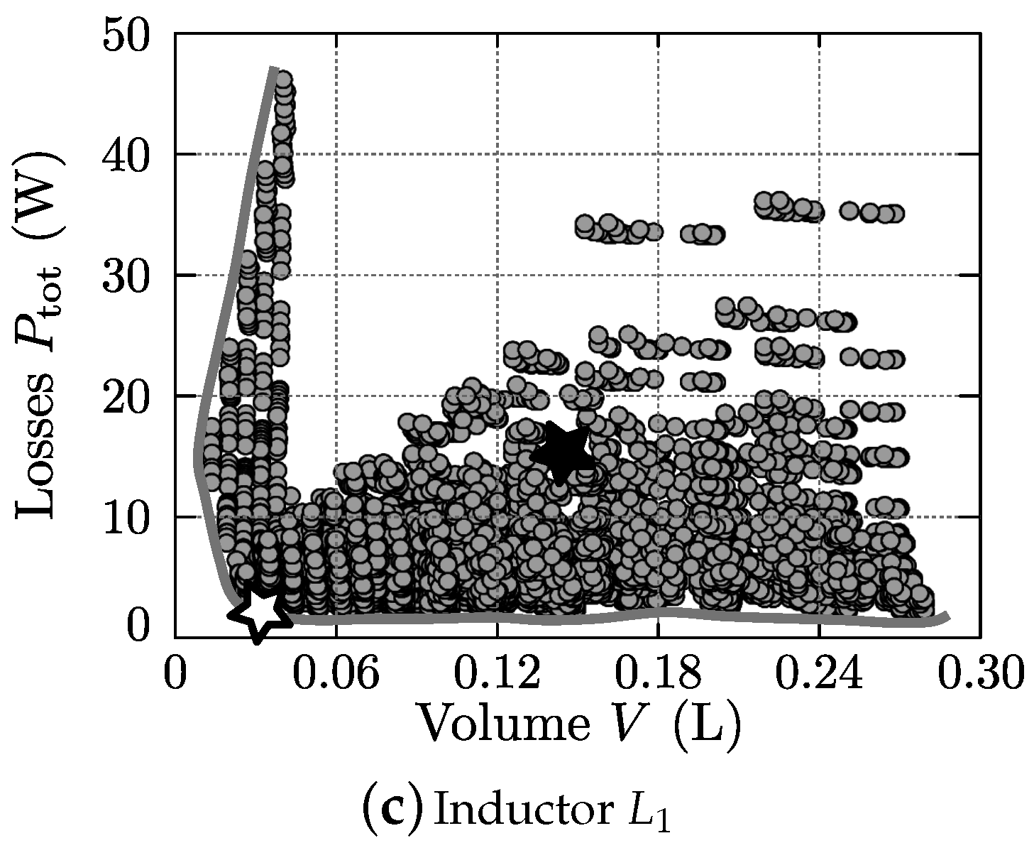
4.2.3. Optimization Results
For each magnetic element of the DAB, the outcome of the optimization is a two-dimensional performance space, showing the losses at nominal operating conditions versus the (boxed) volume of the component. Figure 14a–c, respectively depict the resulting performance spaces for the HF transformer and for inductors and . The designs that are chosen for the hardware realization of the transformer and of inductor are marked with ✩. As these designs are located in the corner point of the so called “Pareto Front”, they are an optimal trade-off between efficiency and power density. It should be noted that the hardware realization of , marked with ★, is a duplicate of the HF transformer with one of the two windings removed and with the air gap length adapted according to the calculated inductance value . The realization of is thus non-optimal, and is referred to as the “prototype” (prot.) design. A better solution would be to use the design marked with ✩, which is referred to as the “optimal” (opt.) design. The detailed parameter values of the transformer and inductor designs are listed in Table A6, Table A7 and Table A8 of Appendix A.2, where Table A8 lists the values for both the “prot.” and the “opt.” design of . The implication of using the improved design “opt.” for on the converter performance is further discussed in Section 5.

Figure 14.
Two-dimensional losses vs. volume performance spaces for (a) the high-frequency (HF) ac-link transformer; (b) inductor ; (c) inductor , calculated for nominal DAB operating conditions.
4.3. Output Filter Capacitors
4.3.1. Low-Frequency (LF) Output Filter Capacitors
Since the DAB handles the double line frequency component of the converter’s ac input power, a LF filter capacitor is placed at the converter’s dc output side (see Figure 1), limiting the output voltage ripple. Assuming unity power factor, where the ac input current and input voltage are in phase, the output voltage ripple is calculated as:
where (≈) is the constant output power component, the angular frequency of the grid, and the average dc output voltage of the converter. As a result, the amplitude of the output voltage ripple is equal to .
In the final hardware demonstrator, the LF output filter capacitance is realized using three 390 F, 500 V dc, electrolytic capacitors (ELCOs), type EETED2W391EA, from Panasonic, Kadoma/Osaka, Japan, which are placed in parallel. This leads to a total LF output filter capacitance value of F. For nominal conditions, i.e., V, A, and V, this results in an very acceptable output voltage ripple amplitude of V. The worst case (i.e., at V, A, and V) ripple amplitude is V, which is still less than 4% of the output voltage.
For the electrolytic LF output filter capacitors, with a diameter of 35 mm and a height of 40 mm (single capacitor), the total boxed volume is 0.147 L. The part of the SR’s fan that does not faces heat sink fins is facing the LF filter capacitors, which are thereby cooled. Consequently, an additional volume of 0.024 L is added to the LF capacitor’s volume for the system volume calculation in Section 5. Remind that this part of the SR’s fan is not taken into account in the volume of the SR’s cooling system, see Section 4.1.4.
4.3.2. High-Frequency (HF) Output Filter Capacitors
Besides the electrolytic LF capacitors, small HF filter capacitors are placed at the output of the DAB in order to bypass the HF components of the DAB output current . The HF filter capacitance value is realized using seven 1.5 F, 630 V dc, metallized polypropylene MKP film capacitors, type B32674D6155, from TDK-EPCOS, Minato, Tokyo, Japan, which are placed in parallel. This leads to a total HF output filter capacitance value of F and a maximum HF output voltage ripple amplitude of less than 2 V. With a width of 31.5 mm, a depth of 12.5 mm, and a height of 19 mm (single capacitor), the total boxed volume is 0.052 L.
4.3.3. Capacitor Losses
Losses in the LF filter capacitors are caused by their equivalent series resistance (ESR) and leakage current. The ESR value listed in the datasheet of the employed 390 F EETED2W391EA ELCOs from Panasonic is 0.34 Ω at 120 Hz. According to the datasheet, the leakage current of a single capacitor is calculated as (A), with C the capacitance value in F and V the capacitor voltage. Consequently, the total power loss in the LF capacitors is calculated as:
where is the RMS value of the current in a single capacitor. The factor 3 is applied since three capacitors are placed in parallel. Since the leakage current of polypropylene film capacitors is very low, the losses in the EPCOS HF capacitors are mainly caused by the ESR, producing a total loss of less than 0.5 W, which can be neglected.
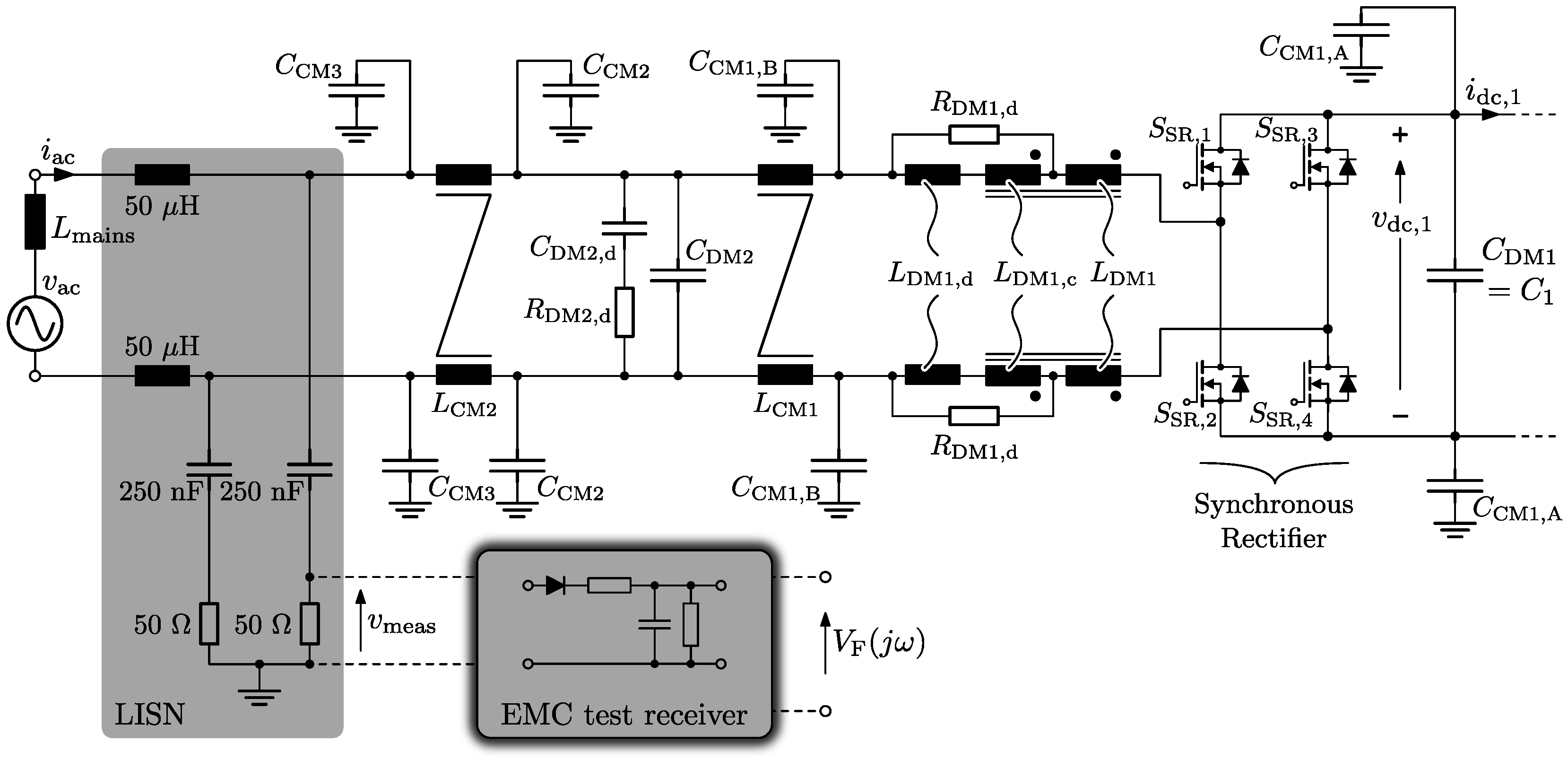
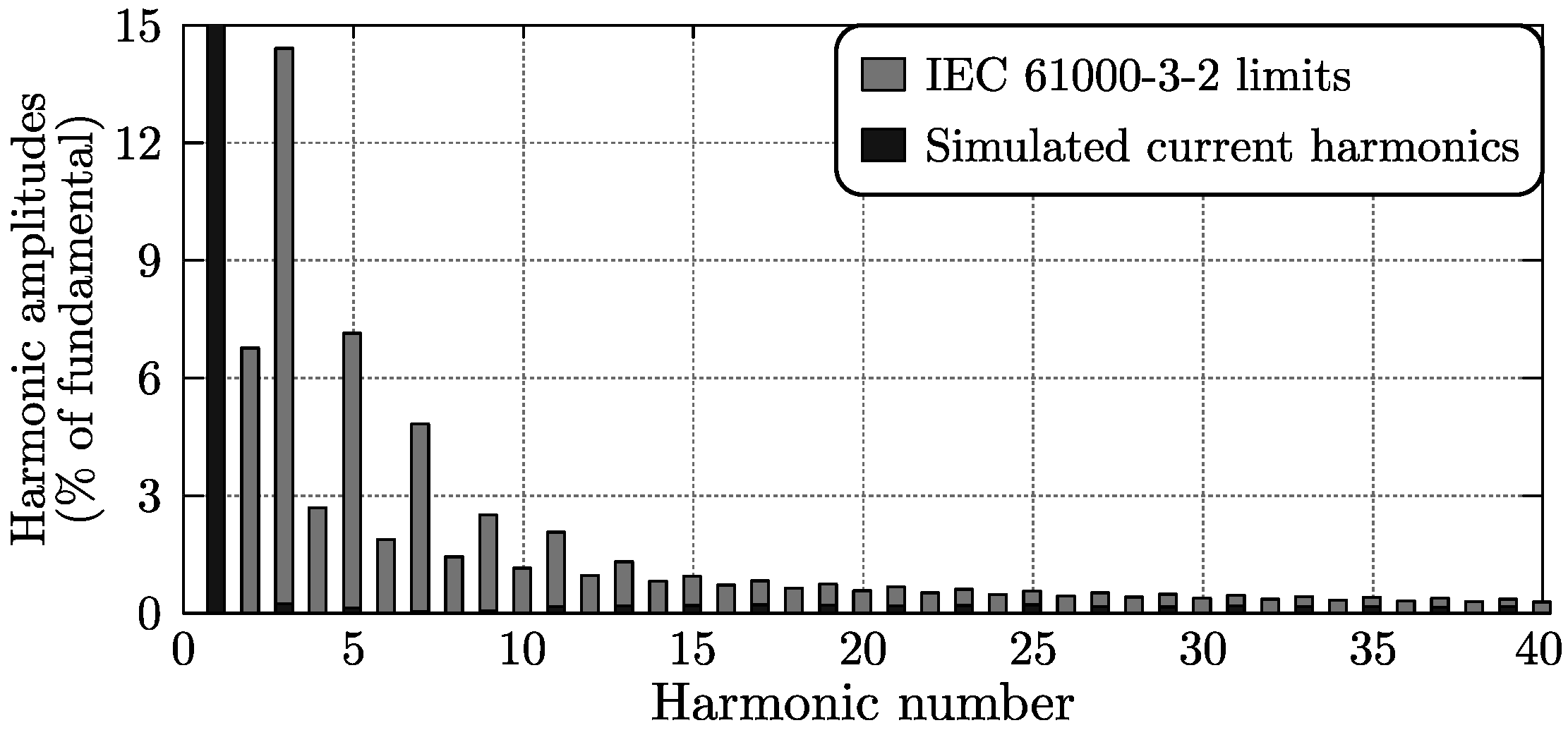
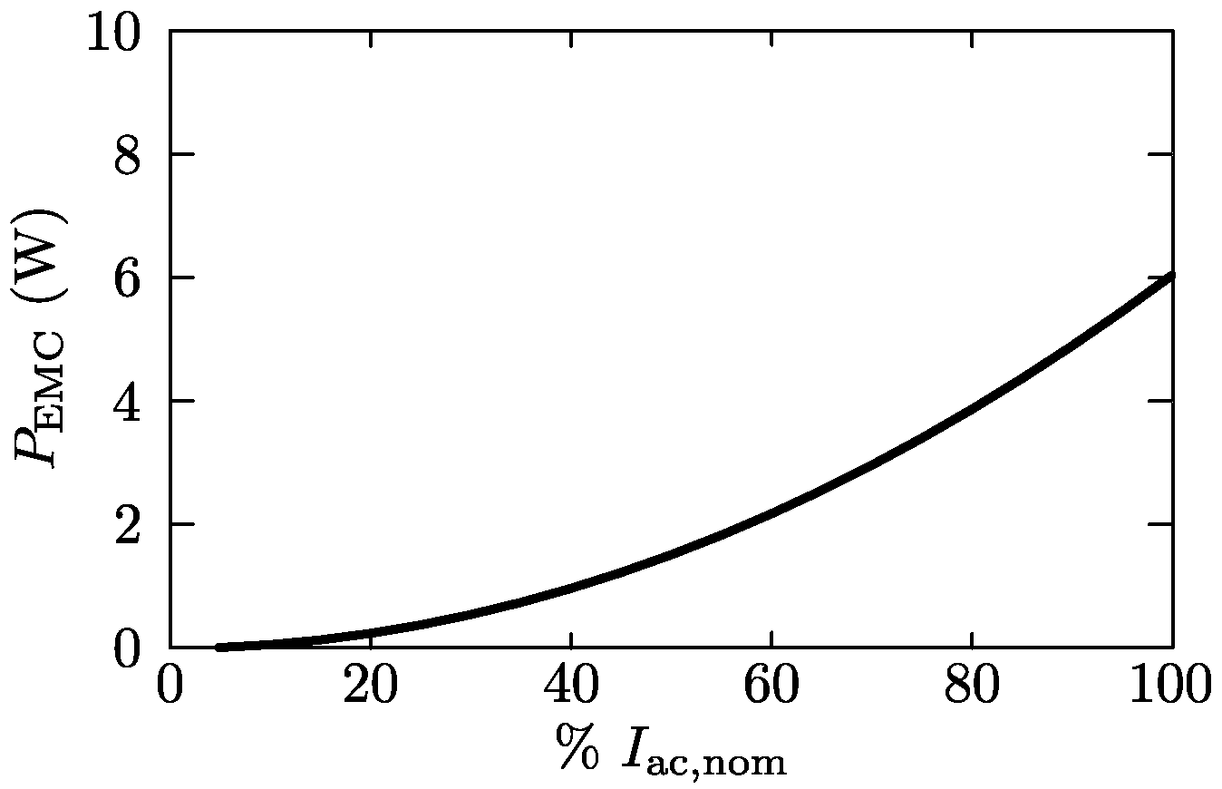
4.4. Electromagnetic Compatibility (EMC) Input Filter
In order to comply with the CISPR 22 Class B standard [43] for conducted emission (CE), an electromagnetic compatibility (EMC) filter is designed. Thereby, a differential mode (DM) filter is required to attenuate the HF components of the DAB input current (see Figure 1), and a common mode (CM) filter for suppressing the CM noise on the earth wire.
4.4.1. Differential Mode (DM) Filter Design
The DM EMC input filter is designed according to the procedure outlined in [44], and conform the guidelines given in [45] regarding filter damping, in order to comply with the CISPR 22 Class B standard [43] in the frequency range of 150 kHz–30 MHz. The employed procedure includes the correct modeling of the line impedance stabilization network (LISN) and of the EMC test receiver (see Figure 15), i.e., conform the CISPR 16 standard [46]. This enables a prediction of the measurement results and thus gives the basis for the calculation of the required attenuation and for the filter design. The video-filtered quasi-peak (QP) values at the output of the EMC test receiver need to be lower than the CISPR 22 Class B limit . For the case where no DM filter is present the most critical QP value is found to be dBV at a corresponding frequency of kHz, at which the Class B limit value is equal to dBV. Therefore, the required attenuation of the DM filter, including a margin of 6 dB, is equal to:
Figure 15.
Schematic of the differential mode/common mode (DM/CM) electromagnetic compatibility (EMC) filters, connected to the synchronous rectifier of the ac-dc converter. Also shown are the line impedance stabilization network (LISN) and the EMC test receiver.
Note that the simulations are performed under nominal operating conditions, i.e., at the nominal ac input voltage of V, the nominal ac input current of A, and an output voltage of V. Also note that towards the dc side of the DAB’s input bridge, the bridge current is rectified into , doubling the frequency. Therefore, and due to operation with variable switching frequency, the value of kHz for can be explained.
The DM filter needs to provide the required attenuation so that, in combination with an appropriate CM filter, the converter complies with the standards. Thereby, control-oriented aspects have to be considered as well, ensuring a satisfactory operation of the converter. Using the recursive design procedure outlined in [44], the two-stage DM filter structure shown in Figure 15 turns out to be most appropriate for achieving these goals (The components of the DM filter in Figure 15 are indexed “DM”, i.e., “DM1” for the first filter stage and “DM2” for the second filter stage. The capacitive part of the first filter stage is effectively realized by the HF dc-link capacitor ). In order to provide sufficient damping of the filter resonances without decreasing the attenuation in the frequency range that is relevant for compliance with the CISPR 22 Class B standard [43], for each filter stage an (optimized) passive damping network is employed. Thereby, a series inductor damping network with coupled inductors is selected for the first filter stage while a parallel capacitor damping network is used for the second filter stage. The resulting values and specifications of the employed DM filter components are listed in Table A9 of Appendix A.3. Note that the second filter stage is formed by capacitance in combination with the LISN ( Ω, nF, H, see Figure 15) and the mains inductance , i.e., no discrete inductor is present.
Figure 16 shows the simulated (nominal operating conditions) video-filtered quasi-peak (QP) values (indicated by a “✩”), along with the CISPR 22 Classes A and B limits and the lower boundary value after insertion of the designed DM input filter and under the assumption of zero mains impedance (Note that the curve is obtained as the square root of the sum of the squares of the RMS values of all harmonic components located within the resolution bandwidth (RBW) of the EMC test receiver [44]). It can be seen that the critical output value (indicated by a “★”) is 6.67 dB lower than the Class B limit , meaning that compliance with the CISPR 22 Class B standard is achieved. Furthermore, the simulated low-frequency harmonics of the mains current , which in the case at hand need to be below the limits defined in the IEC 61000-3-2 standard [30] for Class A equipment, are depicted in Figure 17 and are well below the limits.
Figure 16.
Simulation of the quasi-peak (QP) measurement after insertion of the designed differential mode (DM) input filter and under the assumption of zero mains impedance. Also shown is the absolute lower boundary for the measurement result and the conducted emission (CE) limits according to CISPR 22 Classes A and B.
Figure 17.
Simulated low-frequency harmonics of the mains current and the IEC61000-3-2 limits.
4.4.2. Common Mode (CM) Filter Design
In order to successfully design a common mode (CM) filter that suppresses the CM noise on the earth wire, an equivalent CM noise-source model is required [47]. Thereby, detailed knowledge of the relevant parasitic impedances, through which the CM currents circulate, is essential. As a result, the design of the CM EMC filter is mostly performed after the realization of a first converter prototype system. The parasitic impedances can then be identified through impedance measurements and a CM noise propagation model can be derived. Consequently, several design iterations of the prototype system and/or the CM filter might be required until compliance with CISPR 22 Class B standard for conducted emission (CE) is obtained. Therefore, and as it is the DM filter and not the CM filter which mainly defines the EMC filter volume, the low-load power factor, and the dynamics of the system, here the detailed modeling of the CM filter is omitted. Nevertheless, a CM filter has been included in the converter hardware but, however, the selection of the filter architecture and the determination of the CM component values are based on intuition rather than on modeling and optimization. As can be seen from Figure 15, in which the components of the CM filter are indexed “CM” (i.e., “CM1” for the first, “CM2” for the second, and “CM3” for the third filter stage), a three-stage CM EMC filter structure is employed. The final values and specifications of the CM filter components used in the converter prototype system are listed in Table A10 of Appendix A.3.
4.4.3. EMC Filter Losses and Volume
The hardware realization of the CM and DM EMC input filter can be seen in the picture of the prototype system presented in Section 5. With a width of 132 mm, a height of 72 mm, and a depth of 25 mm, the total boxed volume of the filter board is 0.238 L. This volume includes the converter’s ac connection terminals and an ac fuse, the converter’s dc connection terminals and a dc fuse, a 2-electrode surge arrestor (type EC600-X, EPCOS), and several metal oxide varistors. An additional volume of 0.042 L is occupied by six CM filter capacitors that are placed on another PCB, yielding a total EMC filter volume of 0.279 L. Since the leakage current of polypropylene film capacitors is very low, the losses in the EPCOS HF EMC filter capacitors are mainly caused by the ESR, producing a total loss of less than 0.4 W. Consequently, the losses in the EMC filter capacitors can be neglected. The same goes for the losses (less than 0.1 W) in damping resistors and , and for the core losses of the DM inductors. Therefore, the main contributors to the overall losses of the EMC input filter are the losses due to dc resistance of the CM and DM inductor windings.
4.4.4. Implementation of the Controller
The control hardware consists of an on-board FPGA (field-programmable gate array), in particular the ALTERA EP3C25E144C8N CYCLONE III (Altera, San Jose, CA, United States), which is operated with a clock frequency of 62.5 MHz and programmed in the VHDL hardware description language. The FPGA is responsible for generating the PWM gate drive signals, for reading in the current and voltage measurement peripherals (A/D converters), and for ‘fast’ overcurrent and overvoltage protection. Moreover it communicates over Ethernet with an off-board PC-based Real-Time Target (RTT). The RTT can be programmed and operated through Matlab/Simulink (MathWorks, Natick, MA, United States) where the PI current controller, the ‘slow’ protection, the start-stop procedures, and the control parameter generation are implemented. The Real-TimeWorkshop (MathWorks, Natick, MA, United States) automatic code generator translates the Matlab/Simulink model into C-code which is executed by the RTT.
The cascaded control structure used to control the switching-cycle averaged DAB input current according to Equation (2) is shown in Figure 18 (A more extensive description of the control structure used can be found in [25], also discussing some ‘advanced’ features that are implemented in the hardware, such as switching-delay compensation and variable dead-time generation). The dashed lines indicate which part of the controller hardware performs each particular task. The measured quantities (index ‘m’) that are available in the PFGA as digital signals are also indicated in Figure 18. For testing of the prototype system a fixed dc voltage was applied to the output of the DAB. Optionally, an outer PI voltage controller can be used to control the output voltage required by the dc load.
Figure 18.
Control structure employed to control the switching-cycle averaged DAB input current according to Equation (2).
The PI current control loop outputs set-current in order to control based on the measured value and a reference value which is generated using a Phase Locked Loop (PLL) and calculation of Equation (2) based on the amplitude set-point of the ac input current and the requested power flow direction . In the test setup, and are directly inputted by the user but they can also origin from an external source such as a battery management system or a vehicle power management system. The control parameters needed by the DAB to effectively generate set-current are determined using lookup tables which are calculated for the whole converter’s operating range, as explained in Section 3.2. Thereby, modulation parameters and switching frequency are determined based on and using linear table interpolation. Finally, the modulator function calculates the frequency counter and the bridge-leg gate counters: . These, as well as the enable signals and the SR state , are inputted to the FPGA PWM-generation modules. Enable signals and origin from the ‘slow’ protection and start/stop/runtime units while the SR state is defined by:
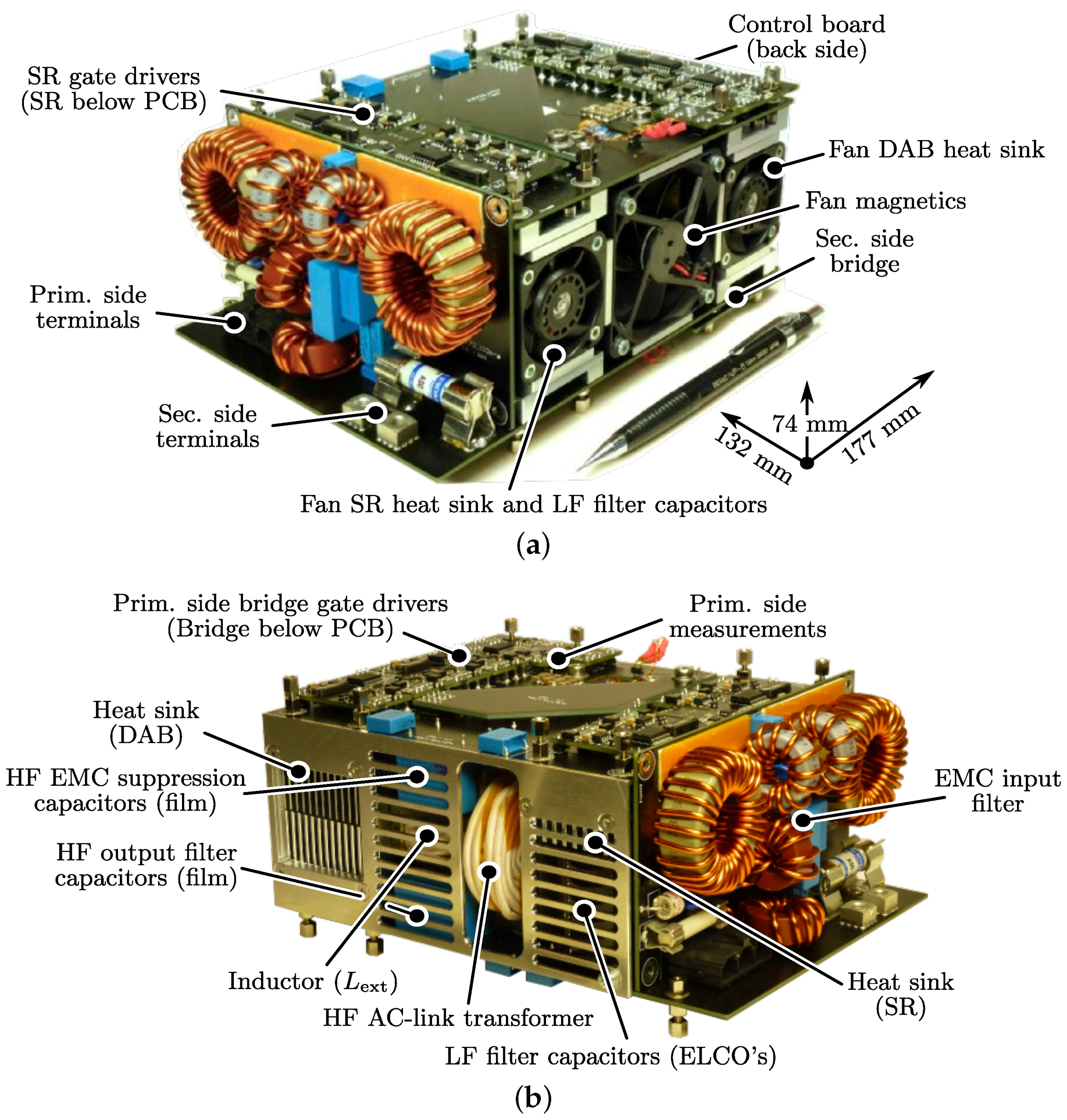
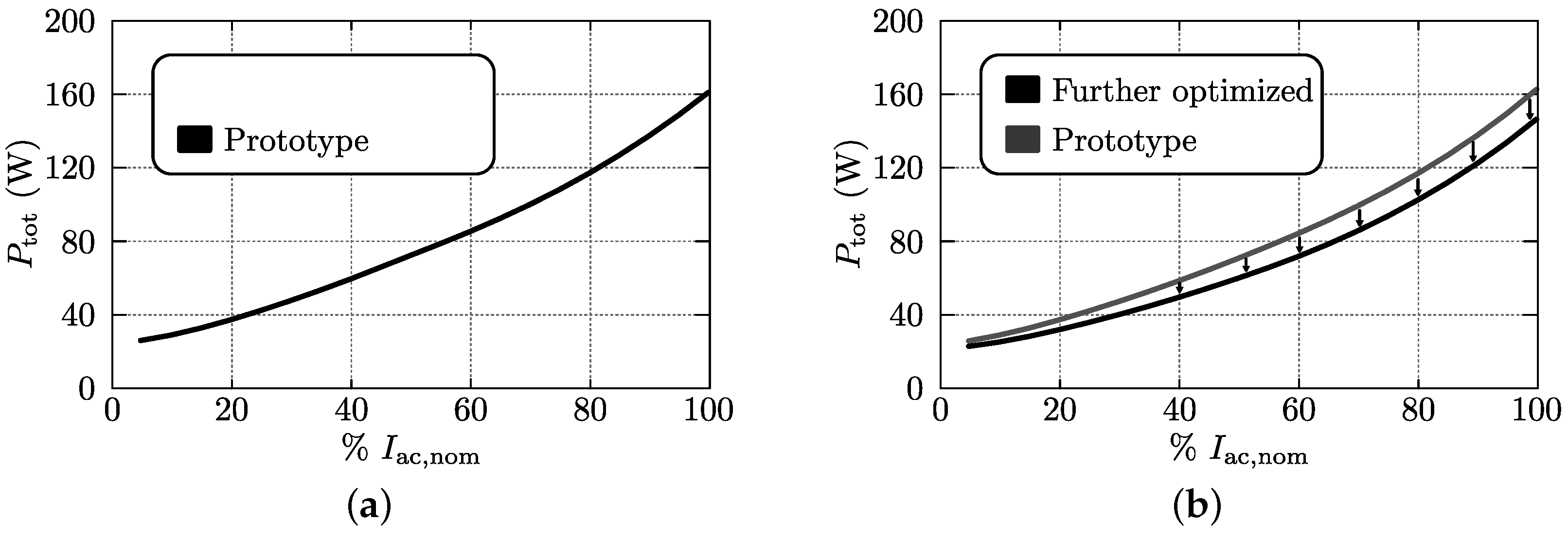
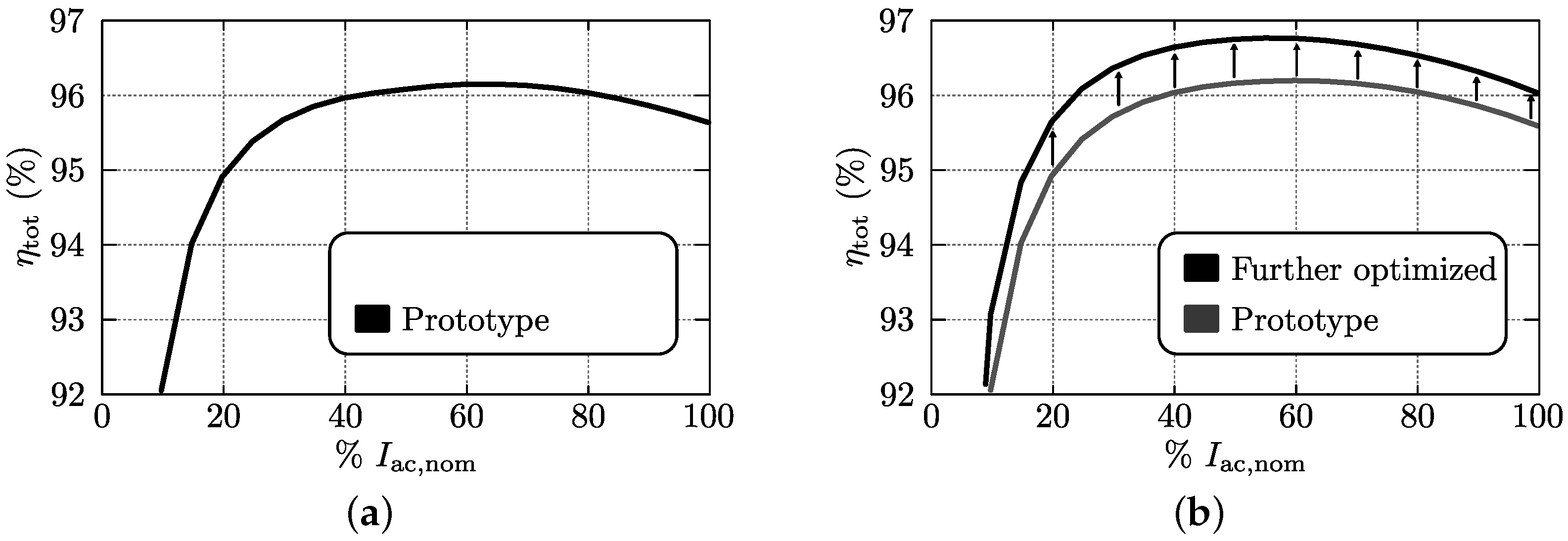
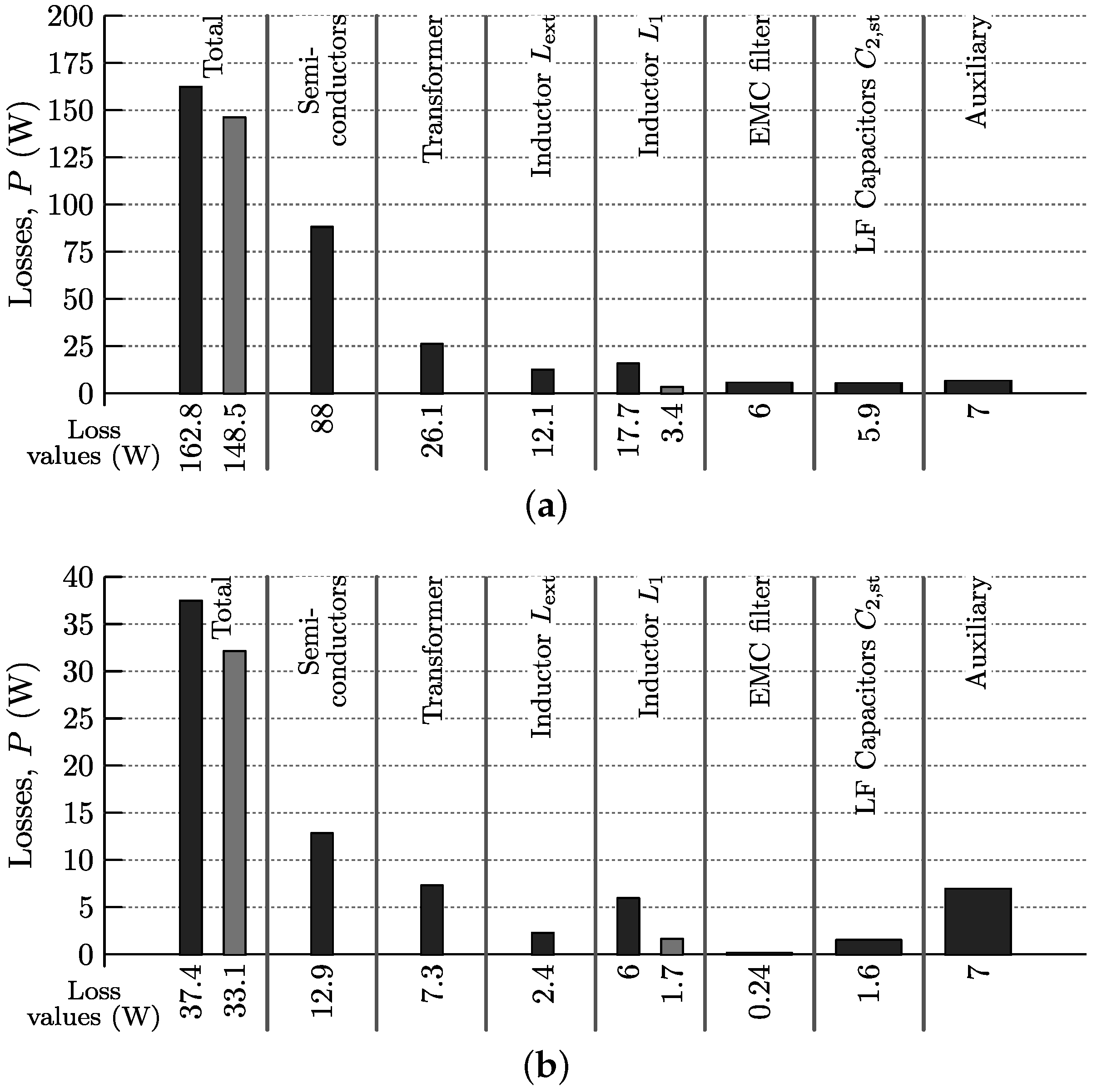
5. Hardware Demonstrator and Calculated Performance
Based on the loss and volume models, and on the results of the component optimizations presented in Section 4, in this section the performance of the 1-S DAB ac-dc converter is calculated in terms of losses (and efficiency) and volume (and power density). The results are obtained under the assumption of C ambient temperature since this has also been the test condition (see Section 6). The 3.7 kW hardware demonstrator, being realized in accordance with the design and optimization results of Section 4, is shown in Figure 19. It should be mentioned that the primary-side commutation inductance was originally not included in the hardware design. During testing was connected to the converter with the screws that are located on the top power PCB. Nevertheless, the volume of this inductor is included in the results for the system’s volume and power density. Below, the calculated performance is presented for two converter designs which only differ from each other by the implementation of the primary-side commutation inductor :
- Converter design A; prototype converter; uses the design “prot.” (prototype) for . This is how the hardware demonstrator is implemented;
- Converter design B; further optimized; uses the improved design “opt.” (optimal) for (see Section 4.2.3). This design yields higher conversion efficiencies and power density compared to converter design A.
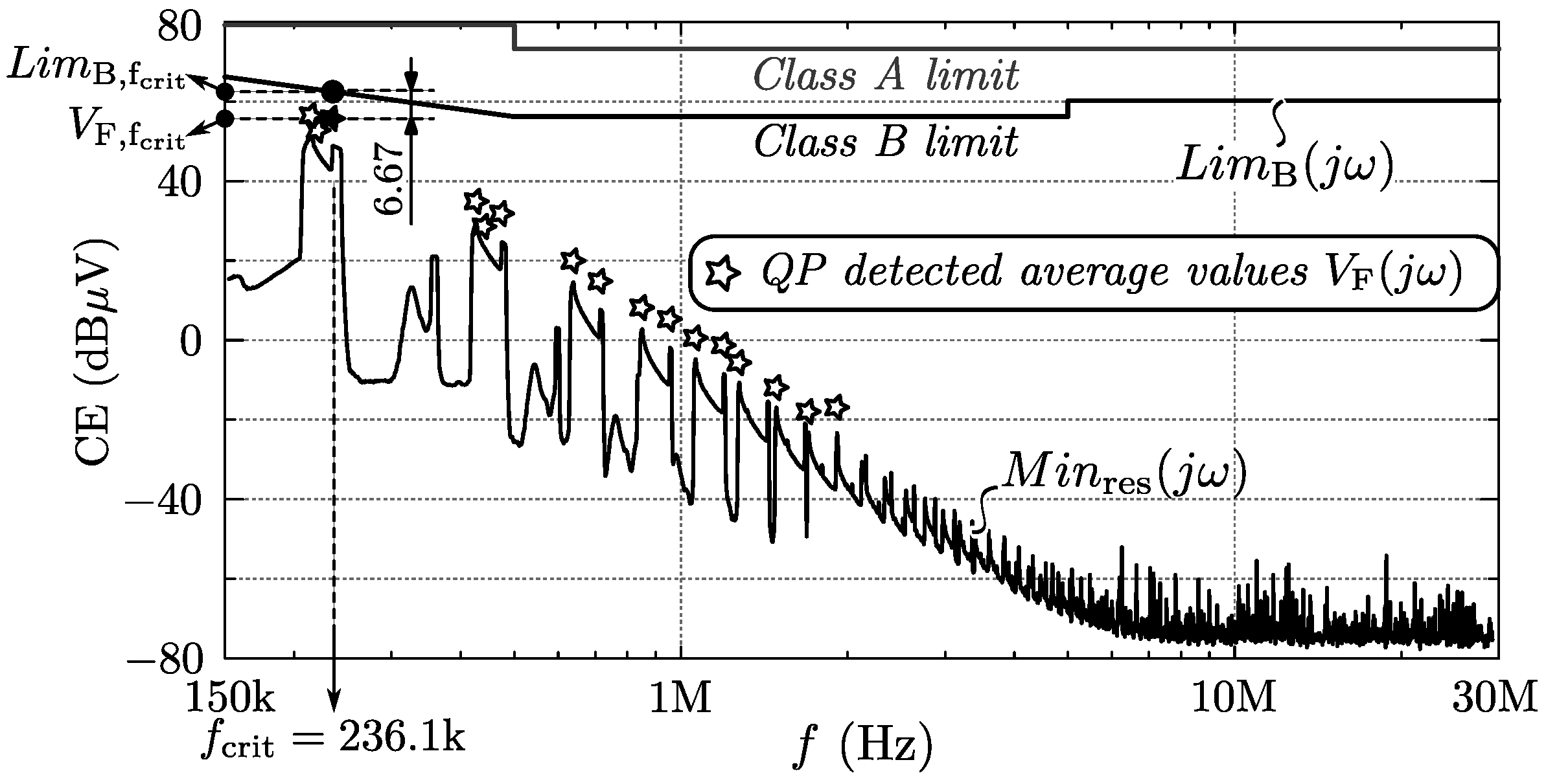
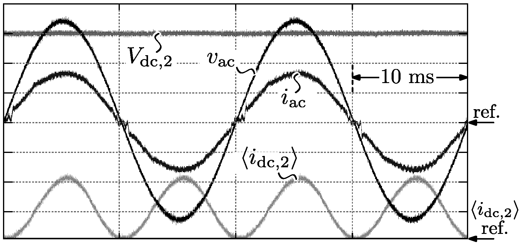
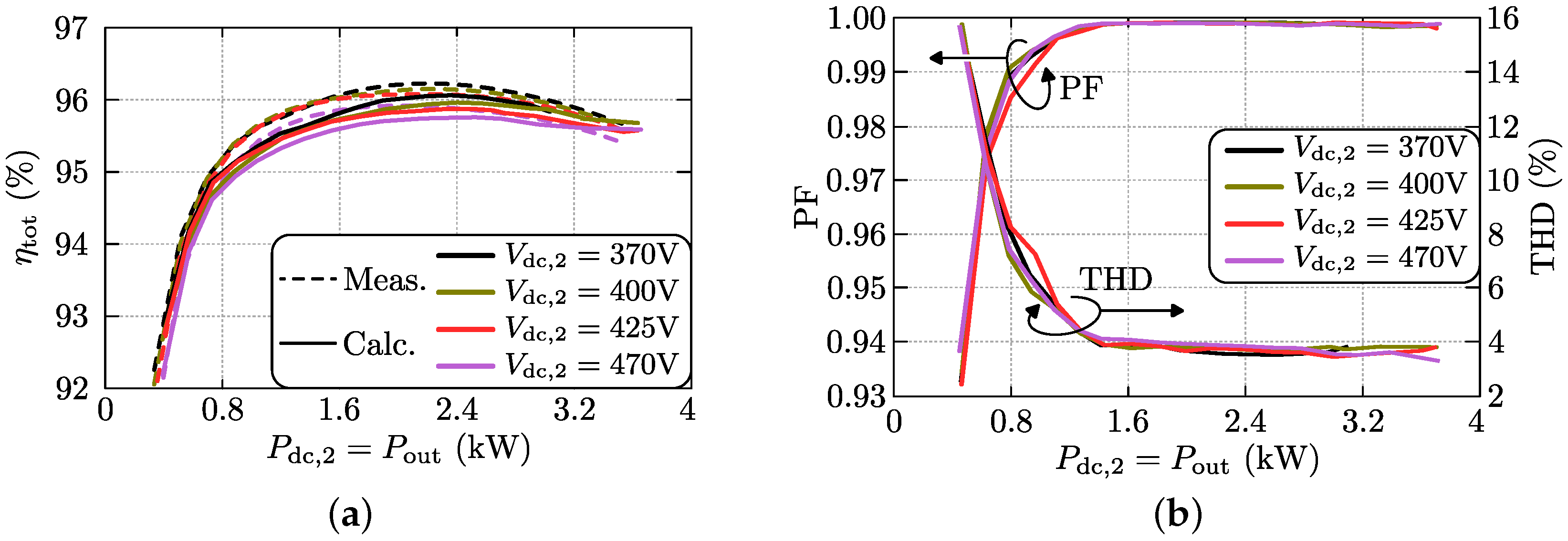
Figure 19.
The 3.7 kW, 1-S (single-stage), single-phase, bidirectional, and isolated DAB ac-dc hardware demonstrator: (a) Front-right view; (b) Front-left view.
The losses of the individual functional elements of the converter are presented in Figure B1, Figure B2, Figure B3, Figure B4 and Figure B5 of Appendix B. They are shown as function of the ac input current , which is expressed as percentage of its nominal value A. Each figure is obtained for the nominal ac input voltage of V and the nominal dc output voltage of V. In Figure B3 it can be seen that the improved design “opt.” for performs significantly better than the design “prot.” (prototype converter), implying that a substantial performance enhancement of the hardware demonstrator would be possible by replacing .
By summation of the losses of the individual components, the overall converter losses are calculated which are shown in Figure 20 for both converters designs A (prototype; see Figure 20a) and B (further optimized; see Figure 20b). As expected, the latter design yields a substantial overall loss reduction. Note that the calculated overall converter losses include the auxiliary power losses, which comprise the power consumption of the fans and of the control board. These losses are estimated to be approximately 7 W. Figure 21 shows the resulting overall conversion efficiency, which for design A (prototype; see Figure 21a) is above 95% for input powers higher than 20% of the nominal input power, with a very flat efficiency curve and thus a high partial-load efficiency. The peak efficiency is around 96.1% and the efficiency at nominal input power approximately 95.6%. From Figure 21b it is clear that, at all power levels, an important efficiency enhancement is feasible (up to around 0.8%) when considering converter design B with optimized inductor .
Figure 20.
Calculated total losses of the 1-S DAB ac-dc converter implemented according to (a) converter design A (prototype converter) and (b) converter design B (further optimized).
Figure 21.
Calculated efficiency of the 1-S DAB ac-dc converter implemented according to (a) converter design A (prototype converter) and (b) converter design B (further optimized).
Figure 22 shows the loss contribution of the different converter components for both converter designs A (prototype; dark gray bars) and B (further optimized; light gray bars). Figure 22a corresponds with the nominal ac input voltage of V, the nominal ac input current of A, and the nominal dc output voltage of V. Figure 22b corresponds with the same voltage conditions but reduced ac input current of A.
Figure 22.
Loss contribution of the different converter components for both converter designs A (prototype; dark gray bars) and B (optimized; light gray bars) at V, V for (a) (100% power) and (b) (20% power).
Figure 23 shows the volume contribution of the different converter components for both converter designs A (prototype; dark gray bars) and B (further optimized; light gray bars), calculated using the boxed component volumes derived in Section 4. The bars “total, excl. other” represent the summation of the component volumes while the bars “total, incl. other” represent the total boxed volume of the complete converter system, including the “dead space” and the volume of the remaining electronic components such as the measurement circuits, the PCBs, and the gate drive units. The volume reduction of 0.107 L achieved for converter design B results from the smaller size of the optimized primary-side commutation inductor .
Figure 23.
Volume contribution of the different converter components for both converter designs A (prototype; dark gray bars) and B (optimized; light gray bars).
The power density values (ρ) that correspond with the total volumes in Figure 23, calculated for the nominal input power of 3.7 kW, are listed in Table 3. A high power density of approximately 2 kW/L is achieved for the prototype converter (i.e., design A) while the power density of the improved converter design (i.e., design B) is around 2.1 kW/L. When only considering the volume occupied by the main converter components, i.e., neglecting the “dead space” and the volume occupied by the measurement circuits, PCBs, and gate drive units, the power densities are respectively 2.5 and 2.7 kW/L. This means that there is still room for reducing the total volume of the system by a more effective assembly of the components. By dividing the volume value “total, excl. other” by the volume value “total, incl. other”, the packing factor is obtained, being a measure of how “good” the different components are assembled. The packing factors for converter designs A and B are respectively and (see Table 3).
Table 3.
Converter power density values (at 3.7 kW, nominal input power).
6. Measurements
The 3.7 kW hardware demonstrator shown in Figure 19 is successfully tested within the full power range (up until an output power of 3.7 kW), showing ac waveforms with little distortion, and which are in very good agreement with the waveforms obtained from simulations. For illustration, Figure 24 depicts the measured waveforms at the ac and dc side of the converter at nominal ac input voltage of V, nominal ac input current of A and 450 V dc output voltage. The conversion efficiency and the converter’s ac input power quality are evaluated using the Yokogawa WT3000 precision power analyzer, having a power accuracy reading of .
Figure 24.
Measured waveforms at the ac and dc side of the converter at nominal ac input voltage of V, nominal ac input current of A and 450 V dc output voltage. Voltage and current scale: : 100 V/div., : 12.5 A/div., : 150 V/div., : 7.5 A/div.
Figure 25 shows the measured performance of the converter with regard to the reached efficiency and with regard to the quality of the ac input power. The measured efficiency (Figure 25a; solid lines) corresponds well with the efficiency calculated in Section 5 (see dashed lines). Although the trends match very well, a slight discrepancy (mostly less than 0.4%) can be noticed between the calculated and the measured efficiencies. This might require further refinement of the loss models developed in Section 4, especially regarding possible non-zero ZVS losses of the MOSFETs. The measured efficiencies are higher than 95% within the major part of the output power range, with a very flat efficiency curve and thus a high partial-load efficiency. The peak efficiency is around 96.1% and the efficiency at nominal output power approximately 95.6% (see curve for the nominal output voltage of V). As predicted by the calculations, only a minor difference (around 0.25%–0.3% at maximum) can be noticed between the efficiency curves at different output voltages, i.e., the efficiency is highest for the lowest output voltage and lowest for the highest output voltage. Furthermore, as can be seen in Figure 25b a (true) power factor (PF) close to unity, and a low total harmonic distortion (THD) of the ac input current of around 4%, are obtained within the major part of the output power range and within the whole output voltage range. This makes that, regarding conversions efficiency, system power density, PF, and THD, the converter requirements specified in Table 1 of the introduction are achieved, confirming the competitiveness of the investigated 1-S DAB ac-dc converter.
Figure 25.
Measurement of (a) the efficiency and (b) the total harmonic distortion (THD) and (true) power factor (PF). The measurements are taken at the nominal ac input voltage of V, in the complete power range (up to 3.7 kW output power), and at different dc output voltages.
For completeness, Figure 26 compares the efficiency of the presented 1-S DAB ac-dc converter (black line; converter A) with the efficiency of two state-of-the-art dual-stage converter systems reported in literature. The efficiency obtained is substantially higher than that of the converter presented in [48] (converter B; Si MOSFETs and SiC diodes), while the converter presented in [49] (converter C) has the highest efficiency but, however, is not bidirectional. The power density reached with converter A (2 kW/L, this work) is substantially higher than the 0.66 kW/L power density of converter B while converter C has the highest power density of 2.5 kW/L. A characteristic comparison of the three converter systems is given in Table 4.
Figure 26.
Comparison of the efficiency of the presented 1-S DAB ac-dc converter (black line; converter A) and the efficiency of two state-of-the-art dual-stage converter systems reported in literature: converter B presented in [48] and converter C presented in [49].
Table 4.
Characteristic comparison of the presented 1-S DAB ac-dc converter (converter A) and the two state-of-the-art dual-stage converter systems reported in literature: converter B presented in [48] and converter C presented in [49].
Lastly, in Figure 27 and Figure 28, measured switching waveforms (see Figure 27b and Figure 28b) of the ac-link currents and voltages are shown, and match very well with the corresponding simulations (see Figure 27a and Figure 28a). The measurements are performed when applying dc voltages at both the input (ac-side) and output (dc-side) terminals of the DAB ac-dc converter, i.e., regarding two different operating points as detailed in the figure captions.
Figure 27.
(a) Calculated and (b) measured HF ac-link currents and voltages at V, A, V, where rad., rad., rad., kHz (mode 1 operation). Voltage and current scale, : 25 V/div., : 150 V/div., : 10 A/div.
Figure 28.
(a) Calculated and (b) measured HF ac-link currents and voltages at V, A, V, where rad., rad., rad., kHz (mode 2 operation). Voltage and current scale, : 150 V/div., : 150 V/div., : 20 A/div.
7. Conclusions
In this paper, a single-stage (1-S) converter approach is analyzed to realize a single-phase, bidirectional, isolated ac-dc converter, combining all functionalities into one conversion stage and thus enabling a cost-effective efficiency and power density increase compared to traditional dual-stage (2-S) ac-dc converters. The converter topology consists of a quasi-lossless synchronous rectifier followed by an isolated DAB dc-dc converter, putting a small filter capacitor in between.
In a first step, the operating principle/conditions of the 1-S ac-dc converter are presented, the available modulation parameters and relevant switching modes of the DAB are detailed, and the method used for calculating an efficient full-operating-range ZVS modulation scheme is summarized. The selection of the high-level circuit variables such as the switching frequency, the inductance values, and the transformer’s turns ratio is outlined as well.
To show the performance potential of the investigated 1-S DAB ac-dc converter, a comprehensive design procedure and multi-objective optimization with respect to efficiency and power density is presented, using detailed loss and volume models. The models and procedures are verified by a 3.7 kW hardware demonstrator, interfacing a 400 V dc-bus with the single-phase 230 V, 50 Hz utility grid. A high power density of approximately 2 kW/L is achieved for the prototype converter, which is implemented with all silicon (Si) MOSFETs. Moreover, measured efficiencies are higher than 95% within the major part of the output power range, with a very flat efficiency curve and thus a high partial-load efficiency. The peak efficiency is around 96.1% and the efficiency at nominal output power approximately 95.6%. The measured efficiency corresponds well with the calculated efficiency, showing only a slight discrepancy of mostly less than 0.4%. This might require further refinement of the loss models, especially regarding possible non-zero ZVS losses of the MOSFETs. Furthermore, a (true) power factor (PF) close to unity, and a low total harmonic distortion (THD) of the ac input current of around 4%, are obtained within the major part of the output power range and within the whole output voltage range. This makes that, regarding conversions efficiency, system power density, PF, and THD, the predefined (automotive) converter requirements are met.
Lastly, the performance of the presented 1-S DAB ac-dc converter is compared with the performance of two state-of-the-art dual-stage converter systems reported in literature. Therefrom, it can be concluded that the achieved efficiency and power density are very close to the absolute state-of-the-art, confirming the competitiveness of the investigated 1-S converter architecture, especially since it is shown that a further efficiency increase of up around 0.8% and a further power density increase of 0.1 kW/L is feasible by a simple improvement of one of the inductor designs (i.e., commutation inductor ). Evidently, an even higher efficiency and/or power density is enabled by use of gallium nitride (GaN) or silicon carbide (SiC) semiconductor devices.
Acknowledgments
Costs to publish this paper in open access are covered by the Electromechanics and Power Electronics (EPE) group of the Eindhoven University of Technology (TU/e). The major part of this work was carried out in the framework of the doctoral (Ph.D.) studies of Jordi Everts at the division of Electrical Energy and Computer Architectures (ELECTA) of the University of Leuven (KU Leuven; Leuven, Belgium) under supervision of Johan Driesen. The research of Jordi Everts was partly funded by a Ph.D. grant of the Institute for the Promotion of Innovation through Science and Technology in Flanders (IWT Vlaanderen). The author also wants to acknowledge Tiphase N.V. (Leuven, Belgium), and in particular Jeroen Van den Keybus for the support provided.
Author Contributions
Jordi Everts developed the models, performed the analysis, designed and built the prototype, conceived and designed the experiments, performed the experiments, analyzed the data, and wrote the paper.
Conflicts of Interest
The authors declare no conflict of interest.
Abbreviations
The following abbreviations are used in this manuscript:
| 1-S | Single-Stage |
| 2-S | Dual-Stage |
| BEV | Battery Electric Vehicle |
| CE | Conducted Emission |
| CM | Common Mode |
| CSPI | Cooling System Performance Index |
| DAB | Dual Active Bridge |
| DM | Differential Mode |
| ELCO | Electrolytic Capacitor |
| EMC | Electromagnetic Compatibility |
| ESR | Equivalent Series Resistance |
| FPGA | Field-Programmable Gate Array |
| HF | High-Frequency |
| iGSE | improved Generalized Steinmetz Equation |
| LF | Low-Frequency |
| LISN | Line Impedance Stabilization Network |
| MOSFET | Metal Oxide Semiconductor Field-Effect Transistor |
| PF | Power Factor |
| PFC | Power Factor Correction |
| PHEV | Plug-in Hybrid Electric Vehicle |
| QP | Quasi-Peak |
| RBW | Resolution Bandwidth |
| SR | Synchronous Rectifier |
| TCM | Triangular Current Mode |
| THD | Total Harmonic Distortion |
| V2G | Vehicle-to-Grid |
| ZVS | Zero Voltage Switching |
Appendix A. Supplement to Section 4
Appendix A.1. Semiconductors and Heat Sinks
Table A1.
Most relevant parameters of the FCH76N60NF high-voltage super-junction MOSFETs employed in the DAB and the STY112N65M5 MDmesh V power MOSFETs employed in the SR.
| Quantity | Value (FCH76...) | Value (STY112...) | Condition | Description |
|---|---|---|---|---|
| (V) | 600 | 650 | C | Drain to source blocking voltage |
| (A) | 72.8 | 96 | C | Continuous drain current |
| (A) | 46 | 61 | C | Continuous drain current |
| (K/W) | 0.23 | 0.2 | - | Thermal resistance, junction to case |
| (mΩ) | 28.7 ( A) | 19 ( A) | V, C | Static drain to source on-resistance (typ.) |
| (A) | 76 | 96 | C | Maximum continuous drain to source diode forward current |
| (nC) | 230 | 350 | V | Total gate charge (typ.) |
| (C) | 1.8 ( A) | 17 ( A) | V | Reverse recovery charge |
| (ns) | 200 ( A) | 570 ( A) | V | Reverse recovery time |
| - | TO-247 | Max247 | - | Package |
| MOSFET Type | ||||||
|---|---|---|---|---|---|---|
| FCH76N60NF | A, V | C, V | ||||
| STY112N65M5 | A, V | C, V | ||||
Table A3.
Coefficients (, and , ) and values for and , required to evaluate (23) for the used MOSFETs.
| MOSFET Type | ||||||
|---|---|---|---|---|---|---|
| FCH76N60NF | 25 C | 38 A | ||||
| STY112N65M5 | 25 C | 48 A |
Table A4.
Performance indices and parameter values that result from the optimization of the heat sink of the DAB (geometry with dual-sided base plate, cf. Figure 10). Top inset: result of the optimization, bottom inset: heat sink used in the final prototype converter.
| Predef. Values | Calc. Optimal Values | |||||||
|---|---|---|---|---|---|---|---|---|
| L (mm) | c (mm) | d (mm) | b (mm) | n | s (mm) | t (mm) | k | |
| Optimum | 99.8 | 37 | 6 | 40.3 | 14 | 1.9 | 1 | 0.6482 |
| (L) | (L) | (L) | (K/W) | (K/W) | (W/K·L) | |||
| 0.2279 | 0.2918 | 0.399 | 0.7142 | 0.3571 | 9.5967 | |||
| L (mm) | c (mm) | d (mm) | b (mm) | n | s (mm) | t (mm) | k | |
| Prototype | 99.8 | 37 | 6 | 40.3 | 13 | 2.1 | 1 | 0.6774 |
| (used for calc.) | (L) | (L) | (L) | (K/W) | (K/W) | (W/K·L) | ||
| 0.2279 | 0.2918 | 0.399 | 0.7298 | 0.3649 | 9.3907 | |||
Table A5.
Performance indices and parameter values that result from the optimization of the heat sink of the SR (geometry with single-sided base plate, cf. Figure 11). Top inset: result of the optimization, bottom inset: heat sink used in the final prototype converter.
| Predef. Values | Calc. Optimal Values | |||||||
|---|---|---|---|---|---|---|---|---|
| L (mm) | c (mm) | d (mm) | b (mm) | n | s (mm) | t (mm) | k | |
| Optimum | 104 | 10 | 5 | 36 | 14 | 1.6 | 1 | 0.608 |
| (L) | (L) | (L) | (K/W) | (K/W) | (W/K·L) | |||
| 0.0624 | 0.0767 | 0.1227 | 1.4372 | 1.4372 | 9.0741 | |||
| L (mm) | c (mm) | d (mm) | b (mm) | n | s (mm) | t (mm) | k | |
| Prototype | 104 | 10 | 5 | 36 | 9 | 2.5 | 1.5 | 0.625 |
| (used for calc.) | (L) | (L) | (L) | (K/W) | (K/W) | (W/K·L) | ||
| 0.0624 | 0.0767 | 0.1227 | 1.7264 | 1.7264 | 7.5542 | |||
Appendix A.2. Magnetic Elements of the DAB: Inductors and Transformer
Table A6.
Design values for the HF ac-link transformer.
| Variable | Value | Description |
|---|---|---|
| 1 | turns ratio | |
| 6 | number of turns (primary-side winding) | |
| 6 | number of turns (secondary-side winding) | |
| (H) | 0.76 | primary-side leakage inductance |
| (H) | 0.76 | secondary-side leakage inductance |
| (H) | 62.1 | magnetizing inductance, which is equal to the secondary-side commutation inductance |
| (mm) | 0.234 | air gap length |
| 700 | number of strands in a Litz bundle (primary-side winding) | |
| 700 | number of strands in a Litz bundle (secondary-side winding) | |
| (m) | 80 | strand diameter (primary-side winding) |
| (m) | 80 | strand diameter (secondary-side winding) |
| 2 | number of paralleled Litz bundles (primary-side winding) | |
| 2 | number of paralleled Litz bundles (secondary-side winding) | |
| - | no | interleaving of the windings |
| - | N97 | core material |
| - | EELP58 | core type/combination |
| - | 2 | number of stacked core combinations |
| (m) | 0.076 | total core length |
| (L) | 0.143 | boxed volume of the transformer |
Table A7.
Design values for the external series inductor .
| Variable | Value | Description |
|---|---|---|
| 4 | number of turns | |
| (H) | 12.2 | inductance value |
| (mm) | 0.603 | air gap length |
| 1458 | number of strands in a Litz bundle | |
| (m) | 71 | strand diameter |
| 1 | number of paralleled Litz bundles | |
| - | N97 | core material |
| - | EELP38 | core type/combination |
| - | 3 | number of stacked core combinations |
| (m) | 0.076 | total core length |
| (L) | 0.0661 | boxed volume of the inductor |
Table A8.
Design values for the primary-side commutation inductor . Both the values for the “prot.” and the “opt.” design of are listed.
| Variable | Value, “opt.” | Value, “prot.” | Description |
|---|---|---|---|
| 13 | 6 | number of turns | |
| (H) | 62.1 | 62.1 | inductance value |
| (mm) | 0.92 | 0.234 | air gap length |
| 184 | 700 | number of strands in a Litz bundle | |
| (m) | 50 | 80 | strand diameter |
| 2 | 2 | number of paralleled Litz bundles | |
| - | N97 | N97 | core material |
| - | EELP32 | EELP58 | core type/combination |
| - | 3 | 2 | number of stacked core combinations |
| (m) | 0.061 | 0.076 | total core length |
| (L) | 0.0358 | 0.143 | boxed volume of the inductor |
Appendix A.3. EMC Input Filter
Table A9.
Differential mode (DM) EMC input filter components.
| Component | Value | Quantity | Specification |
|---|---|---|---|
| Filter Stage 1 | |||
| /, coupled inductor | 34.6/1.64 H | 2 | Magnetics, High Flux 60, CO58083A2, 23:5 turns, 11 AWG wire |
| , inductor | 6.9 H | 2 | Magnetics, MPP60, CO55351A2, 13 turns, 11 AWG wire |
| , X2 capacitor (MKP) | 13.2 F | 6 in par. | EPCOS-B32923E3225, 2.2 F, 305 V |
| , SMD resistor | 0.19 Ω | 2 × 2 in par. | 0.38 Ω-1 W |
| Filter Stage 2 | |||
| = | 0 ... 300 H | - | Mains inductance |
| , X2 capacitor (MKP) | 1 F | 1 | EPCOS-B32923C3105, 1 F, 305 V |
| , X2 capacitor (MKP) | 0.47 F | 1 | EPCOS-B32922C3474, 0.47 F, 305 V |
| , SMD resistor | 20 Ω | 2 in ser. | 10 Ω-0.33 W |
Table A10.
Common mode (CM) EMC input filter components.
| Component | Value | Quantity | Specification |
|---|---|---|---|
| AC-Side: Filter Stage 1 | |||
| , inductor | 0.34 mH @ 100 kHz | 1 | Vacuumschmelze VAC, VITROPERM 500F, L2020-W409, 2 × 5 turns, 11 AWG wire |
| , Y2 capacitor (MKP) | 6.8 nF | 2 × 1 | EPCOS-B32021A3682, 6.8 nF, 300 V |
| , Y2 capacitor (MKP) | 2.2 nF | 2 × 1 | EPCOS-B32021A3222, 2.2 nF, 300 V |
| AC-Side: Filter Stage 2 | |||
| , inductor | 0.34 mH @ 100 kHz | 1 | Vacuumschmelze VAC, VITROPERM 500F, L2020-W409, 2 × 5 turns, 11 AWG wire |
| , Y2 capacitor (MKP) | 10 nF | 2 × 1 | EPCOS-B32022A3103, 10 nF, 300 V |
| AC-Side: Filter Stage 3 | |||
| , Y2 capacitor (MKP) | 1 nF | 2 × 1 | EPCOS-B32021A3102, 1 nF, 300 V |
| DC-Side | |||
| , Y2 capacitor (MKP) | 13.6 nF | 2 × 2 | EPCOS-B32021A3682, 6.8 nF, 300 V |
Appendix B. Supplement to Section 5
Figure B1.
(a) Calculated total losses generated by all semiconductors of the DAB and SR; (b) Junction temperatures of all semiconductors, i.e., the switches of active bridge 1 (DAB), of active bridge 2 (DAB), and of the SR.
Figure B2.
Calculated losses of (a) the HF ac-link transformer and (b) the external series inductor .
Figure B3.
Calculated losses of the commutation inductor implemented according to (a) design “prot.” (prototype converter) and (b) the improved design “opt.” (further optimized).
Figure B4.
(a) Calculated total losses of the LF output filter capacitors ; (b) Calculated total losses of the HF output filter capacitors .
Figure B5.
Calculated total losses of the EMC input filter.
References
- Haghbin, S.; Lundmark, S.; Alakula, M.; Carlson, O. Grid-Connected Integrated Battery Chargers in Vehicle Applications: Review and New Solution. IEEE Trans. Ind. Electron. 2013, 60, 459–473. [Google Scholar] [CrossRef]
- Yilmaz, M.; Krein, P.T. Review of Battery Charger Topologies, Charging Power Levels, and Infrastructure for Plug-In Electric and Hybrid Vehicles. IEEE Trans. Power Electron. 2013, 28, 2151–2169. [Google Scholar] [CrossRef]
- Dong, D.; Cvetkovic, I.; Boroyevich, D.; Zhang, W.; Wang, R.; Mattavelli, P. Grid-Interface Bidirectional Converter for Residential DC Distribution Systems—Part One: High-Density Two-Stage Topology. IEEE Trans. Power Electron. 2013, 28, 1655–1666. [Google Scholar] [CrossRef]
- Kim, H.S.; Ryu, M.H.; Baek, J.W.; Jung, J.H. High-Efficiency Isolated Bidirectional AC-DC Converter for a DC Distribution System. IEEE Trans. Power Electron. 2013, 28, 1642–1654. [Google Scholar] [CrossRef]
- Rocabert, J.; Luna, A.; Blaabjerg, F.; Rodriguez, P. Control of Power Converters in AC Microgrids. IEEE Trans. Power Electron. 2012, 27, 4734–4749. [Google Scholar] [CrossRef]
- Fan, Y.; Zhu, W.; Xue, Z.; Zhang, L.; Zou, Z. A Multi-Function Conversion Technique for Vehicle-to-Grid Applications. Energies 2015, 8, 7638–7653. [Google Scholar] [CrossRef]
- Singh, B.; Singh, B.N.; Chandra, A.; Al-Haddad, K.; Pandey, A.; Kothari, D.P. A Review of Single-Phase Improved Power Quality AC-DC Converters. IEEE Trans. Ind. Electron. 2003, 50, 962–981. [Google Scholar] [CrossRef]
- Sekar, A.; Raghavan, D. Implementation of Single Phase Soft Switched PFC Converter for Plug-in-Hybrid Electric Vehicles. Energies 2015, 8, 13096–13111. [Google Scholar] [CrossRef]
- Marxgut, C.; Biela, J.; Kolar, J.W. Interleaved triangular current mode (TCM) resonant transition, single phase PFC rectifier with high efficiency and high power density. In Proceedings of the International Power Electronics Conference (IPEC 2010), Sapporo, Japan, 21–24 June 2010; pp. 1725–1732.
- Marxgut, C.; Krismer, F.; Bortis, D.; Kolar, J.W. Ultraflat Interleaved Triangular Current Mode (TCM) Single-Phase PFC Rectifier. IEEE Trans. Power Electron. 2014, 29, 873–882. [Google Scholar] [CrossRef]
- Steigerwald, R.L. A Comparison of Half-Bridge Resonant Converter Topologies. IEEE Trans. Power Electron. 1988, 3, 174–182. [Google Scholar] [CrossRef]
- Steigerwald, R.L.; de Doncker, R.W.; Kheraluwala, M.H. A Comparison of High-Power DC-DC Soft-Switched Converter Topologies. IEEE Trans. Ind. Appl. 1996, 32, 1139–1145. [Google Scholar] [CrossRef]
- Mehdipour, A.; Farhangi, S. Comparison of three isolated bi-directional DC/DC converter topologies for a backup photovoltaic application. In Proceedings of the 2nd International Conference on Electric Power and Energy Conversion Systems (EPECS 2011), Sharjah, UAE, 15–17 November 2011; pp. 1–5.
- Tan, N.M.L.; Abe, T.; Akagi, H. Topology and application of bidirectional isolated DC-DC converters. In Proceedings of the IEEE 8th International Conference on Power Electronics and ECCE Asia (ICPE 2011—ECCE Asia), Jeju, Korea, 30 May–3 June 2011; pp. 1039–1046.
- Krismer, F.; Kolar, J.W. Efficiency-Optimized High-Current Dual Active Bridge Converter for Automotive Applications. IEEE Trans. Ind. Electron. 2012, 59, 2745–2760. [Google Scholar] [CrossRef]
- Wang, Y.C.; Ni, F.M.; Lee, T.L. Hybrid Modulation of Bidirectional Three-Phase Dual-Active-Bridge DC Converters for Electric Vehicles. Energies 2016, 9, 492. [Google Scholar] [CrossRef]
- Hu, S.; Li, X.; Lu, M.; Luan, B.Y. Operation Modes of a Secondary-Side Phase-Shifted Resonant Converter. Energies 2015, 8, 12314–12330. [Google Scholar] [CrossRef]
- Shi, X.; Jiang, J.; Guo, X. An Efficiency-Optimized Isolated Bidirectional DC-DC Converter with Extended Power Range for Energy Storage Systems in Microgrids. Energies 2013, 6, 27–44. [Google Scholar] [CrossRef]
- Norrga, S. A soft-switched bi-directional isolated AC/DC converter for AC-Fed railway propulsion applications. In Proceedings of the International Conference on Power Electronics, Machines and Drives (PEMD 2002), Bath, UK, 4–7 June 2002; pp. 433–438.
- Norrga, S. Experimental Study of a Soft-Switched Isolated Bidirectional AC-DC Converter Without Auxiliary Circuit. IEEE Trans. Power Electron. 2006, 21, 1580–1587. [Google Scholar] [CrossRef]
- Vangen, K.; Melaa, T.; Bergsmark, S.; Nilsen, R. Efficient high-frequency soft-switched power converter with signal processor control. In Proceedings of the IEEE 13th International Telecommunications Energy Conference (INTELEC 1991), Kyoto, Japan, 5–8 November 1991; pp. 631–639.
- Kheraluwala, M.H.; de Doncker, R.W. Single phase unity power factor control for dual active bridge converter. In Proceedings of the IEEE Industry Applications Society Annual Meeting, Toronto, ON, Canada, 2–8 October 1993; Volume 2, pp. 909–916.
- Everts, J.; van den Keybus, J.; Krismer, F.; Driesen, J.; Kolar, J.W. Switching control strategy for full ZVS soft-switching operation of a dual active bridge AC/DC converter. In Proceedings of the IEEE 27th Annual Applied Power Electronics Conference and Exposition (APEC 2012), Orlando, FL, USA, 5–9 February 2012; pp. 1048–1055.
- Jauch, F.; Biela, J. Single-phase single-stage bidirectional isolated ZVS AC-DC converter with PFC. In Proceedings of the 15th International Power Electronics and Motion Control Conference (EPE/PEMC 2012), Novi Sad, Serbia, 3–6 September 2012; pp. LS5d.1-1–LS5d.1-8.
- Everts, J.; Krismer, F.; van den Keybus, J.; Driesen, J.; Kolar, J.W. Optimal ZVS Modulation of Single-Phase Single-Stage Bidirectional DAB AC-DC Converters. IEEE Trans. Power Electron. 2014, 29, 3954–3970. [Google Scholar] [CrossRef]
- Everts, J.; Krismer, F.; van den Keybus, J.; Driesen, J.; Kolar, J.W. Charge-based ZVS soft switching analysis of a single-stage dual active bridge AC-DC converter. In Proceedings of the IEEE Energy Conversion Congress and Exposition (ECCE 2013), Denver, CO, USA, 15–19 September 2013; pp. 4820–4829.
- Weise, N.D.; Basu, K.; Castelino, G.; Mohan, N. A Single-Stage Dual-Active-Bridge-Based Soft Switched AC-DC Converter With Open-Loop Power Factor Correction and Other Advanced Features. IEEE Trans. Power Electron. 2014, 29, 4007–4016. [Google Scholar] [CrossRef]
- Krismer, F.; Kolar, J.W. Closed Form Solution for Minimum Conduction Loss Modulation of DAB Converters. IEEE Trans. Power Electron. 2012, 27, 174–188. [Google Scholar] [CrossRef]
- Everts, J.; Krismer, F.; van den Keybus, J.; Driesen, J.; Kolar, J.W. Comparative evaluation of soft-switching, bidirectional, isolated AC/DC converter topologies. In Proceedings of the IEEE 27th Annual Applied Power Electronics Conference and Exposition (APEC 2012), Orlando, FL, USA, 5–9 February 2012; pp. 1067–1074.
- The International Electrotechnical Commission. Electromagnetic Compatibility (EMC)—Part 3-2: Limits for Harmonic Current Emissions (Equipment Input Current ⩽16 A per Phase); IEC 61000-3-2; IEC, International Electrotechnical Commission: Geneva, Switzerland, 1995. [Google Scholar]
- De Doncker, R.W.; Divan, D.M.; Kheraluwala, M.H. A three-phase soft-switched high power density DC/DC converter for high power applications. In Proceedings of the IEEE Industry Applications Society Annual Meeting, Pittsburgh, PA, USA, 2–7 October 1988; Volume 1, pp. 796–805.
- Infineon Technologies AG. First 650 V Rated Super Junction MOSFET with Fast Body Diode Suitable for Resonant Topologies; Technical Report; Infineon Technologies AG: Neubiberg, Germany, 2011. [Google Scholar]
- Drofenik, U.; Laimer, G.; Kolar, J.W. Theoretical converter power density limits for forced convection cooling. In Proceedings of the International PCIM Europe 2005 Conference (PCIM 2005), Nuremberg, Germany, 7–9 June 2005; pp. 608–619.
- Drofenik, U.; Kolar, J.W. Sub-optimum design of a forced air cooled heat sink for simple manufacturing. In Proceedings of the Power Conversion Conference-Nagoya (PCC 2007), Nagoya, Japan, 2–5 April 2007; pp. 1189–1194.
- Kolar, J.W.; Drofenik, U.; Biela, J.; Heldwein, M.L.; Ertl, H.; Friedli, T.; Round, S.D. PWM converter power density barriers. In Proceedings of the Power Conversion Conference (PCC 2007), Nagoya, Japan, 2–5 April 2007; pp. P-9–P-29.
- Krismer, F. Modeling and Optimization of Bidirectional Dual Active Bridge DC-DC Converter Topologies. Ph.D. Thesis, Swiss Federal Institute of Technology (ETH Zürich), Power Electronic Systems (PES) Laboratory, Zürich, Switzerland, 2010. [Google Scholar]
- Buccella, C.; Cecati, C.; de Monte, F. A Coupled Electrothermal Model for Planar Transformer Temperature Distribution Computation. IEEE Trans. Ind. Electron. 2008, 55, 3583–3590. [Google Scholar] [CrossRef]
- Ferreira, J.A. Analytical Computation of AC Resistance of Round and Rectangular Litz Wire Windings. IEE Proc. B Electr. Power Appl. 1992, 139, 21–25. [Google Scholar] [CrossRef]
- Sullivan, C.R. Optimal Choice for Number of Strands in a Litz-Wire Transformer Winding. IEEE Trans. Power Electron. 1999, 14, 283–291. [Google Scholar] [CrossRef]
- Mühlethaler, J.; Kolar, J.W.; Ecklebe, A. Loss modeling of inductive components employed in power electronic systems. In Proceedings of the IEEE 8th International Conference on Power Electronics (ICPE ECCE Asia 2011), Jeju, Korea, 30 May–3 June 2011; pp. 945–952.
- Mühlethaler, J.; Kolar, J.W.; Ecklebe, A. A novel approach for 3D air gap reluctance calculations. In Proceedings of the IEEE 8th International Conference on Power Electronics (ICPE ECCE Asia 2011), Jeju, Korea, 30 May–3 June 2011; pp. 446–452.
- Venkatachalam, K.; Sullivan, C.R.; Abdallah, T.; Tacca, H. Accurate prediction of ferrite core loss with nonsinusoidal waveforms using only steinmetz parameters. In Proceedings of the IEEE Workshop on Computers in Power Electronics, Mayaguez, Puerto Rico, 3–4 June 2002; pp. 36–41.
- International Special Committee on Radio Interference. Limits and Methods of Measurement of Radio Disturbance Characteristics of Information Technology Equipment–Publication 22; IEC, International Special Committee on Radio Interference: Geneva, Switzerland, 1993. [Google Scholar]
- Nussbaumer, T.; Heldwein, M.L.; Kolar, J.W. Differential Mode Input Filter Design for a Three-Phase Buck-Type PWM Rectifier Based on Modeling of the EMC Test Receiver. IEEE Trans. Ind. Electron. 2006, 53, 1649–1661. [Google Scholar] [CrossRef]
- Erickson, R.W. Optimal single resistors damping of input filters. In Proceedings of the IEEE 14th Annual Applied Power Electronics Conference and Exposition (APEC 1999), Dallas, TX, USA, 14–18 March 1999; Volume 2, pp. 1073–1079.
- International Special Committee on Radio Interference. Specification for Radio Interference Measuring Apparatus and Measurement Methods–Publication 16; IEC, International Special Committee on Radio Interference: Geneva, Switzerland, 1977. [Google Scholar]
- Heldwein, M.L.; Nussbaumer, T.; Kolar, J.W. Common Mode Modelling and Filter Design for a Three-Phase Buck-Type Pulse Width Modulated Rectifier System. IET Power Electron. 2010, 3, 209–218. [Google Scholar] [CrossRef]
- Gautam, D.S.; Musavi, F.; Edington, M.; Eberle, W.; Dunford, W.G. An Automotive Onboard 3.3-kW Battery Charger for PHEV Application. IEEE Trans. Veh. Technol. 2012, 61, 3466–3474. [Google Scholar] [CrossRef]
- Kolar, J.W.; Krismer, F.; Lobsiger, Y.; Muhlethaler, J.; Nussbaumer, T.; Minibock, J. Extreme efficiency power electronics. In Proceedings of the 7th International Conference on Integrated Power Electronics Systems (CIPS 2012), Nuremberg, Germany, 6–8 March 2012; pp. 1–22.
© 2016 by the author; licensee MDPI, Basel, Switzerland. This article is an open access article distributed under the terms and conditions of the Creative Commons Attribution (CC-BY) license (http://creativecommons.org/licenses/by/4.0/).