Abstract
This article describes the design, control, and implementation of a photovoltaic (PV) emulator using two-switch forward-converter topology. The system is designed to emulate the nonlinear electrical behavior of an actual PV panel under different environmental conditions including radiation level and temperature. The emulator provides galvanic isolation and also accurate current modulation to provide a safe yet reliable means of testing PV-related devices and algorithms within a laboratory setting. A dual-loop PI control is proposed to adjust the output current according to voltage feedback (VF), thus making accurate I–V and P–V curves achievable. Besides software simulation, a tailored printed circuit board (PCB) was fabricated. The simulation result demonstrated that the system can achieve a fast response and stable operation, with a maximum error percentage of about 2.1%, indicating high emulation fidelity, thereby providing an attractive platform for various evaluation purposes such as MPPT algorithms, inverters, and EMS.
1. Introduction
There has been a rapid increase in the application of photovoltaic (PV) energy systems for residential, commercial, and industrial demands due to the huge demand for clean renewable energy. Nevertheless, achieving high performance of PV-compatible subsystems e.g., maximum power point tracking (MPPT) strategies, power converters, and energy management systems in dynamic environmental conditions is rather challenging. Classical methods that require the use of real solar panels during testing are often unfeasible due to their dependence on uncontrolled and variable levels of irradiance and temperature.
To address these challenges, PV emulators serve as an attractive solution. Such systems can electronically mimic a solar panel in the laboratory under controlled conditions. With its ability to produce a constant, programmable, and repeatable output, the PV emulator allows rapid development and the testing of a variety of control strategies without requiring direct sunlight or large simulated PV arrays.
In the various emulator structures, power converter-based solutions are flexible and scalable and enable real-time control. Isolated topologies are especially favored for their capability to provide galvanic isolation, safety, and superior control of high-voltage operation. The present study centers around a novel design and control of PV emulator based on two-switch forward-converter topology. This particular configuration has been chosen as it offers enhanced reliability, by avoiding voltage stress on the switching devices, and accurate current control to simulate the I–V curves of an actual solar module.
The primary contribution of this paper is the creation of a real-time PV emulator that includes
- A mathematical computational current generation algorithm using irradiance and temperature inputs;
- A double-loop PI control method for dynamic current output;
- A transformer-isolated forward converter to achieve safety and true power transfer.
In the various emulator structures reported in the literature, power converter-based solutions offer excellent flexibility, scalability, and compatibility with real-time control platforms. Among these solutions, isolated converter topologies are particularly attractive, as they provide galvanic isolation between the input supply and the output terminals of the emulator. This isolation enhances operational safety, improves electromagnetic compatibility, and enables reliable testing of high-voltage PV systems without direct electrical coupling between the source and the device under test. In isolated converters, power is transferred through a high-frequency transformer by means of magnetic coupling, ensuring true energy transmission rather than direct conduction.
The present study focuses on the design and control of a PV emulator based on the two-switch forward-converter topology, which represents a robust and high-performance isolated architecture. Unlike flyback converters that transfer energy indirectly by first storing it in the magnetic core and then releasing it to the load, the two-switch forward converter enables continuous and direct (true) energy transfer from the input source to the load during the conduction interval. This operating principle significantly improves power efficiency, reduces peak current stress, and minimizes core losses and thermal loading, allowing the system to support higher output power levels than flyback-based solutions.
In addition, the two-switch forward topology limits voltage stress on the power switches through effective transformer demagnetization, resulting in improved reliability and long-term stability of the hardware. The presence of a transformer also enables flexible load interfacing, making it possible to safely test and supply multiple loads arranged in parallel or in series, which is not practically achievable with non-isolated buck or boost converters due to grounding constraints and safety limitations. This feature broadens the applicability of the proposed emulator to larger experimental setups, including multi-string PV testing and complex MPPT validation platforms.
The simulation results demonstrate that the proposed emulator can successfully emulate the nonlinear I–V as well as P–V characteristics of a solar panel under different conditions. With the fast transient of the system, which is 35 ms, and its accuracy, it can be used as a first stage platform for testing PV systems in applications where safety and reproducibility are important.
2. Related Work
Photovoltaic (PV) emulators have been increasingly used as tools for R&D and testing of solar energy systems, providing controlled operational conditions to assess converters, MPPT algorithms, and energy management strategies. There are various emulator topologies reported in the recent literature, such as Buck, Boost, Full-Bridge, and Flyback converters [1,2,3]. Isolated topologies among them are seen to be advantageous for applications due to their safety and electromagnetic compatibility advantages, specifically in high-voltage test benches [4,5]. Buck-type emulators have been commonly used because of the ease of implementation, but dynamic tracking and reserve current protection are not always easy to achieve [6,7]. Some boost-based systems are able to accommodate a greater voltage range, but they need to be accurately controlled in rapid irradiance variations [8]. Forward converters, in particular, the two-switch topology, allows speed, voltage clamping, and transformer isolation to be effectively optimized [9,10]. More recent works have focused on incorporating real-time control to follow I–V characteristics under different conditions [11,12,13]. Fast emulation cycles and compatibility with MPPT testing have been achieved by FPGA- and DSP-based implementation [14,15]. In addition, the closed-loop system with adaptive or fuzzy control has been suggested in order to improve accuracy [16,17].
Some works have confirmed hardware realizations based on PCB prototypes. Compact emulators representing dynamic irradiance and temperature influences have been designed/validated experimentally [18,19,20]. In addition, model-based reference generation based typically on the single-diode model of a solar cell further enhanced current output accurracy [21,22].
Various studies have been carried out on HIL-based emulators for which MATLAB/Simulink is used combined with control boards [23,24]. These platforms enable the reproduction of test conditions and help in assessing new inverter topologies or control methods [25,26].
However, in spite of these improvements, the converter is not widely used in the PV emulation literature. Due to its capability of high-frequency operation and efficient energy exchange, it is an attractive candidate for emulator architectures, in particular when interconnected with fast control loops By now, applications in works, including exploring the feasibility of such technology, have begun but validation with a dedicated fabricated PCB or real-time control is very limited and the I–V tracking profile for immediately stabilizing low jump is insufficient.
Through its capability for magnetic energy transfer, galvanic isolation, superior efficiency, reduced device stress, and enhanced load adaptability, the proposed two-switch forward converter emerges as a more powerful and versatile architecture for PV emulation compared to conventional flyback and non-isolated DC–DC converters. This work fills the gap by introducing a complete PV emulator developed on a custom PCB that is built around a two-switch forward-converter topology and validated with dynamic test profiles, yielding new findings for accuracy, stability, and hardware implementability.
3. System Description
The novel two-switch forward-converter topology design of the photovoltaic (PV) emulator has been chosen due to its robustness, inherent galvanic isolation, and capacity for accurately emulating the nonlinear current–voltage characteristics of practical solar panels without risks. The system is intended to be used in laboratory conditions for testing MPPT algorithms, inverter interfaces, and energy management strategies under controlled irradiance and temperature profiles.
3.1. Overview of the Power Architecture
The full block diagram of the emulator system is depicted in Figure 1, which consists of a constant DC input source, a transformer-isolated two-switch forward converter (TSFC), a secondary-side rectifier and filter stage, and a closed-loop control section. The converter has two main power switches (Q1 and Q2) and a high-frequency transformer with primary and secondary windings (L1 and L2) answering to the clamping diodes (D1 and D2) for safely recycling magnetic energy during demagnetization. On the output end, a rectifying diode (D3) and an RC filter (R1, C1) are provided for generating some stable voltage and current. Figure 1 shows the full diagram of the emulator compatible instrument that may be used for real-time emulation of common PV output profiles. This architecture allows standalone validation tests or integration in the context of microgrid test benches.
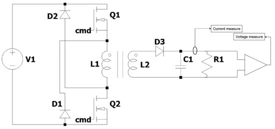
Figure 1.
Block diagram of the proposed PV emulator using a two-switch forward converter.
In the following subsections, we will discuss system accuracy, dynamic response, and emulation fidelity through simulation results and experimental validation.
The design ensures that the output of the emulator can be dynamically modulated to follow the I–V and P–V characteristics of a real PV panel under varying irradiance levels. This modulation is achieved through a real-time control strategy described in the subsequent section.
3.2. Converter Operating Principles
The converter has two separate modes: magnetization (Mode 1) and demagnetization (Mode 2). These modes of operation are displayed in Figure 2 and Figure 3.
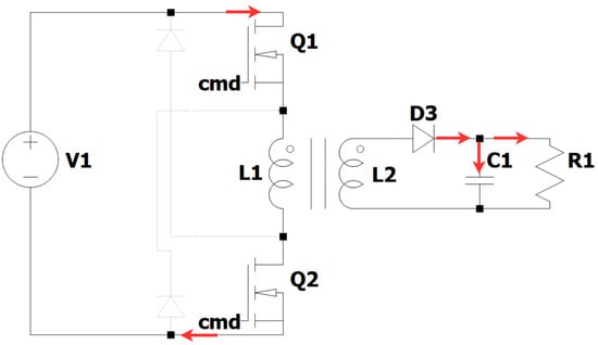
Figure 2.
Mode 1 operation: energy transfer phase with transformer magnetization.
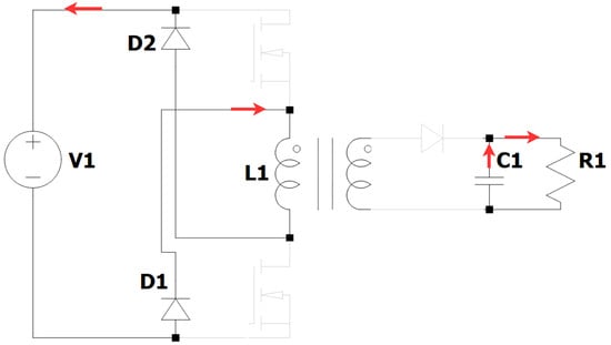
Figure 3.
Mode 2 operation: transformer demagnetization via clamping diodes.
Mode 1: Transformer Magnetization. When all switches Q1 and Q2 are ON at the same time (see Figure 2), V1 is impressed on primary winding L1. As a result, the current inflow magnetizes the transformer core and induces a corresponding voltage at secondary winding L2. The diode D3 is forward biased, and, therefore, the current passes through the load R1 as well as capacitor C1 that it charges. During this period, the transformer delivers power from V S to OUT, and the load current is regulated by manipulating Q1’s and Q2’s duty cycle.
Mode 2: Transformer Demagnetization. If both Q1 and Q2 are turned OFF by the control logic, the converter moves to Mode 2 as presented in Figure 3. The clamp diodes D1 and D2 conduct after demagnetization due to the magnetizing field of the transformer, providing a path for the demagnetization current back to an input source. In this condition, diode D3 is non-conducting and no current is applied from the transformer to the load, except for some energy in the capacitor C1 for a while. This resets the transformer and prevents magnetic saturation and high-voltage stress on the switches.
The alternation between these two modes at a fixed switching frequency allows the emulator to modulate its output in response to external irradiance profiles or control references.
3.3. Custom PCB Design and Hardware Integration
To demonstrate the implementation of the proposed architecture in a realistic environment, we designed a custom two-layer PCB. The structure and arrangement of the components are presented in Figure 4. The board includes the entire power stage electronics, controller and support circuitry, gate drivers, current and voltage sensors, and communication ports. Particular emphasis was placed on the design of PCB traces in order to reduce EMI and parasitic inductance, particularly in the proximity of switching nodes and transformer connection points. A custom-wound transformer on a high-frequency ferrite core was designed for 50 kHz switching, and thermal issues were handled with the help of heatsink main switches and well-considered positioning of power resistors. The sensing blocks directly measure the instantaneous output voltage and current with differential op-amp circuits.
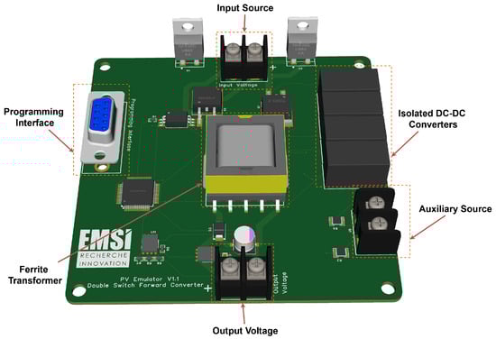
Figure 4.
Printed Circuit Board Overview.
4. Control Strategy and Modeling
The control scheme used in this new PV emulator was designed to accurately reproduce the I–V characteristics of a physical PV module when subjected to changes in solar irradiance and temperature. Here, an emulator output current is periodically adjusted based on the calculated output voltage and a given irradiance–temperature profile. The system is controlled by a closed-loop scheme with an inner current and outer voltage control loops based on dual-loop PI.
Figure 5 shows the internal control loop of the proposed PV emulator that emulates dynamic electrical characteristics of a photovoltaic panel according to ambient temperature and irradiance levels. The method applies real-time measurements of voltage and current sensors and environmental data in the calculation of the photogeneration current using a mathematical model. This value is compared to the real current, and error is reduced using a two-stage PI regulator. Then, the output of the MPPT controller will be presented to a PWM generator, and emulator voltage signal is controlled in order to resemble a real PV source as much as possible while testing and validating systems. The developed PV 1 emulator is based on a custom two-layer PCB, in which the power conversion stage, as well as its control and sensing blocks, together with communication peripherals are integrated. A two-switch forward-converter architecture is used with high-speed power MOSFETs driven by specialized gate driver ICs to achieve stable and also balanced switching of the primary transformer section as presented in Table 1. The transformer uses the EE35 ferrite core chosen in this design to handle the required power level and switching frequency with an operating gap enough for magnetic isolation between input and output connection.
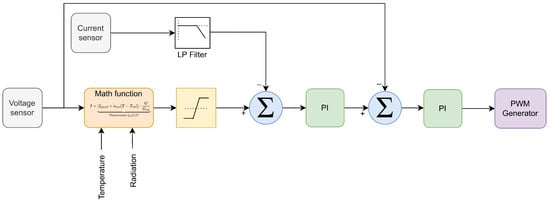
Figure 5.
Dual loop PI controller.

Table 1.
Major components used in the proposed PCB design.
A bulk electrolyc capacitor supplies energy storage and filtering for low-frequency ripple suppression, and a ceramic by-pass capacitor offers high-frequency decoupling. The second rectifying stage features ultra-fast recovery diodes for efficient current conduction and low switching loss. Galvanic isolation of control and power domains is additionally achieved by the implementation of several isolated DC–DC converters, which generate independent auxiliary power supplies for gate-driving and signal conditioning circuitry.
Real-time current acquisition using a Hall-effect sensor (ACS712-05B) provides accurate readings of output current while keeping electrical isolation. Voltage scaling and signal conditioning make use of resistor networks in conjunction with a TL072 operational amplifier, which provides convenient interfacing to the analog-to-digital converters available on microcontrollers. The control programs are written and run on an STM32F030RCT6 microcontroller which is responsible for feedback capture, PI controller regulation, PWM generation as well as interface external communication.
Common interfacing includes programming, control inputs, monitoring outputs, and power terminals, making the emulator easy to incorporate into laboratory test systems.
4.1. PV Model-Based Current Reference Generation
The reference current of the proposed photovoltaic emulator is generated based on the classical single-diode PV mathematical model, which enables accurate reproduction of the nonlinear electrical behavior of real photovoltaic modules under varying irradiance and temperature conditions. The model uses the measured terminal voltage of the emulator and environmental input variables, namely solar irradiance G and temperature T, to compute the output current reference supplied to the inner current control loop.
The photogenerated current is determined by both irradiance and temperature variations and is expressed as
where represents the photogenerated current at standard test conditions (STCs), is the temperature coefficient of the short-circuit current, T is the operating temperature of the PV module, is the reference temperature (25 °C), G is the actual irradiance, and is the reference irradiance (1000 W/m2).
The reverse saturation current of the diode is modeled as a temperature-dependent parameter according to
where is the reverse saturation current at STCs, q is the elementary charge, is the semiconductor band-gap energy, n is the diode ideality factor, and k is Boltzmann’s constant. This relation captures the strong influence of temperature on the diode conduction behavior and, consequently, on the open-circuit voltage of the PV module.
Based on the previous expressions, the output current of the PV module is computed using the well-known Shockley diode equation
where I is the emulator output current and V is the terminal voltage of the emulator. The exponential term represents the nonlinear voltage-dependent behavior of the PN junction.
The calculated current I serves as the reference input for the inner PI current controller, which regulates the duty cycle of the two-switch forward converter to ensure accurate tracking of the desired I–V characteristic. The outer PI voltage control loop adjusts the current reference to maintain operation along the programmed PV curve. Together, these loops guarantee stable steady-state operation and fast dynamic response for the proposed PV emulator across different environmental conditions and load variations.
This modeling framework enables the emulator to reproduce arbitrary user-defined I–V and P–V profiles in real time and provides a flexible platform for evaluating MPPT algorithms, converter control strategies, and energy management systems prior to hardware-in-the-loop or laboratory deployment.
4.2. Dual-Loop Control Architecture
The control block is structured around two cascaded Proportional–Integral (PI) controllers:
- The outer voltage loop continuously monitors the output voltage of the emulator and adjusts the current reference to maintain operation along the PV I–V curve.
- The inner current loop compares the actual output current with the reference and modulates the duty cycle of the two-switch forward converter to enforce accurate current tracking.
This cascade approach improves transient response and stability, particularly under rapidly changing load conditions or simulated irradiance variations. The controller parameters were tuned using classical pole placement and verified through time-domain simulation.
Two PI controllers are employed in the dual-loop control structure. The outer controller (PI1) regulates the voltage loop and generates the reference current required to operate the emulator along the targeted PV I–V characteristic. The inner controller (PI2) tracks this reference current and adjusts the duty cycle of the two-switch forward converter, ensuring a fast dynamic response.
Both PI controllers are characterized by a proportional gain and an integral time constant , as summarized in Table 2. Output saturation limits are implemented to prevent integrator windup and guarantee safe operation of the power stage. The controller gains were tuned in simulation based on classical pole placement principles, targeting fast settling, negligible steady-state error, and zero overshoot during transient operating conditions.
Table 2.
PI controller parameters.
4.3. Switching and PWM Implementation
The proposed PV emulator is controlled with a constant switching frequency pulse width modulation (PWM) method of 50 kHz. And such a switching frequency is actually a trade-off between the requirement of miniaturizing magnetic element and the one for limiting switching losses in power MOSFETs. During both commutation cycles, Q1 and Q2 are turned on together to provide full balanced excitation of the primary transformer. Such symmetric excitation is important in order to avoid an accumulation of magnetic flux error across cycles, which would eventually saturate the core and increase losses or possibly cause device failure.
The oscillation PWM duty cycle is continuously controlled by the inner current control loop of the dual-loop PI structure. Controlling the duty ratio to change in real time allows the converter to accurately adjust the output current, and thus, the emulator voltage–current operation point tracks target PV Iv characteristic at various irradiance and temperature levels. This methodology provides a high tracking precision and can be used under dynamic load or change in reference to smooth the transitions.
A dead-time insertion circuit is employed in the gate driver logic, so that cross-conduction via Q1 and Q2 when switching transitions is prevented. This control arrangement guarantees that one switch is completely OFF before the other has access to turn ON, resulting in the elimination of a shoot-through and increasing reliability of the converter. The dead time is chosen to be long enough to ensure safe switching under worst-case device delays, but short enough so as not to excessively distort the effective duty cycle.
The PWM signals are generated by and the dead time applied by a digital controller which is part of a system hardware. It performs the current and voltage control algorithms at a high sampling speed allowing low-latency computation and high-precision duty-cycle updates, which are essential for stable real-time emulation. This digital representation leads to deterministic timing and, consequently, minimal delay between the control action and the plant response at acceptable additional costs compared to purely analog implementations. Thus, providing additional options for future extensions (adaptive or predictive controller strategies).
4.4. Real-Time Execution and Measurement Feedback
Isolation differential amplifiers are used to measure voltage across the output leads and across current sense resistors. The latter are acquired at high frequency and input to the control algorithm, which runs in real time on a microcontroller or DSP device.
Irradiance and temperature may be manually entered, programmed as a time-varying test pattern, or read from external sensors to simulate actual solar conditions at differing times. This flexibility allows the system to accommodate dynamic PV curve playback and connected MPPT controller or inverter system stress testing.
4.5. Validation of Control Performance
As demonstrated by the experiment results in the Results and Discussion section, this control strategy can guide the emulator to track target I–V or P–V curves well under various conditions. Analog model-driven current reference and active dual-loop control architecture is employed for fast settling time, low steady-state error, as well as smooth transitions during dynamic irradiance variations.
5. Results and Discussion
This section presents a comprehensive analysis of the emulator’s behavior under different operating conditions, including variations in irradiance, temperature, and load. Each set of results offers insight into the accuracy and dynamic performance of the system.
5.1. Static Characteristics with Irradiance Variation
Figure Figure 6 shows the current–voltage (I–V) characteristics obtained at four different irradiances from 400 to 1000 W/m2. Unsurprisingly, larger irradiance yields higher short-circuit current, and there is only a small shift in the open-circuit voltage. Those trends are in agreement with the expected trend for PV cells. The simulated I–V curve at 1000 W/m2 almost coincide with the theoretical reference, and this result verifies that the emulator can accurately replicate the electrical behavior of a real PV panel.
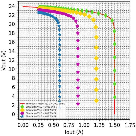
Figure 6.
I–V characteristics for different irradiance levels (400–1000 W/m2).
The P–V curves were determined for the same intensities of illumination and are shown in Figure 7. At higher fluence, the peak power varies linearly with it, and its voltage at maximum power point does not change a lot. These results demonstrate that the emulator can reproduce the anticipated P–V response for varying lighting actions. The superposition of the simulated and theoretical curves at full irradiance confirms again the fidelity and soundness of the model.
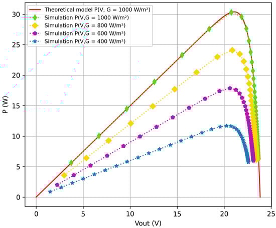
Figure 7.
P–V characteristics under varying irradiance levels.
5.2. Dynamic Response During Load Sweep
For a dynamic analysis on the emulator, a resistive load was changed gradually, and their corresponding output response is displayed in Figure 8. The voltage plot at the top shows a slow decrease as the load is increased. On the other hand, the output current (middle panel) rises accordingly. The lower graph verifies a controlled resistance step down that breadboards in the emulator through large sets of bias points. As a whole, looking at the tests, the system is stable, and there are no noticeable oscillations or lag to be detected whatsoever, which reflects the adequacy of using this control strategy for real-time applications.
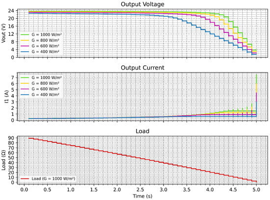
Figure 8.
Dynamic performance under irradiance sweep: output voltage, current, and load resistance.
5.3. Temperature Influence on Static Characteristics
This subsection examines the behavior of the proposed PV emulator under commanded temperature variations in order to evaluate the stability and tracking performance of the control strategy. It is important to clarify that the temperature-dependent curves presented here are based on a user-defined reference profile applied to the emulator model for testing purposes and do not aim to represent the exact physical power–temperature characteristic of a specific commercial PV module. Instead, they illustrate the ability of the proposed topology and PI controller to accurately follow arbitrary temperature-dependent I–V and P–V references, as would be required in practical PV emulation scenarios.
In the adopted test profile, 35 °C was selected as the nominal reference temperature of the emulator, and output power was scaled around this operating point to observe the system’s response under different thermal commands. Figure 6 and Figure 7 display the corresponding P–V and I–V characteristics, respectively, obtained at the configured temperatures. As expected from the emulator structure, variations in temperature modify the voltage level primarily, while the short-circuit current remains only weakly affected. The controller maintains stable operation across all tested temperature commands, with fast convergence to the corresponding reference curves and no observable overshoot or oscillation during steady-state transitions.
These results demonstrate that the proposed two-switch forward converter with dual-loop PI control can accurately reproduce predefined temperature-dependent PV operating characteristics, regardless of the specific temperature profile selected by the user. This flexibility is a key advantage for laboratory testing, where the emulator must be capable of generating customized operating scenarios for PV performance assessment, MPPT validation, and control system benchmarking. The response of the emulator to temperature is illustrated as a function of power output at a specific irradiance level in Figure 9. With the increase in temperature from 25 °C to 65 °C, maximum power diminishes; at around 35 °C, the Pmax (33.51 W) is obtained, as seen in Figure 9. This loss of power is mainly related to the decrease in open-circuit voltage, which is a known phenomenon for PV systems. The results indicate that the emulator reacts properly to thermal changes and can be used to reproduce temperature-dependent PV performances.
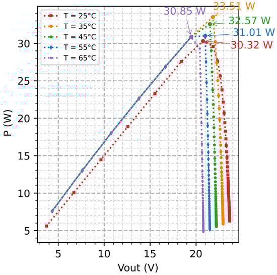
Figure 9.
P–V characteristics under varying temperature levels (25–65 °C).
The I–V characteristics are plotted in Figure 10. Again we see that with increasing temperature, the voltage decreases, whereas the current stays roughly constant. This is expected due to the physical properties of silicon solar cells. The emulator smoothly reproduces the thermal effects so they are not distorted, increasing confidence in control and modeling during its design.
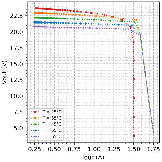
Figure 10.
I–V characteristics under temperature variation.
5.4. Real-Time Operation Under Temperature Changes
To examine in more detail how the system performs in real time, we simulated a decreasing load profile on the emulator at constant fixed temperatures. The results are shown in Figure 11. The voltage and current speed waveforms display the predicted change in electrical response to thermally excited effects. With rising temperature, the voltage profile shifts to a lower voltage, and the current is enhanced slightly. The emulator still faithfully tracks these changes without introducing instability, demonstrating that this approach can be employed for hardware-in-the-loop (HIL) testing and other applications which need final real-time emulation.
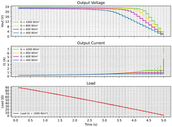
Figure 11.
Dynamic response at different temperatures: output voltage, current, and equivalent load.
5.5. Start-Up Performance Across Multiple Loads
The start-up behavior is a performance index of the power electronics system. The output voltage of the emulator during start-up for resistive loads from 50 Ω to 10 kΩ is illustrated in Figure 12 and Figure 13. In all instances, the output voltage ramps quickly to its final value with little overshoot and good repeatability. The voltage stabilizes at about 25.3 V regardless of the load.
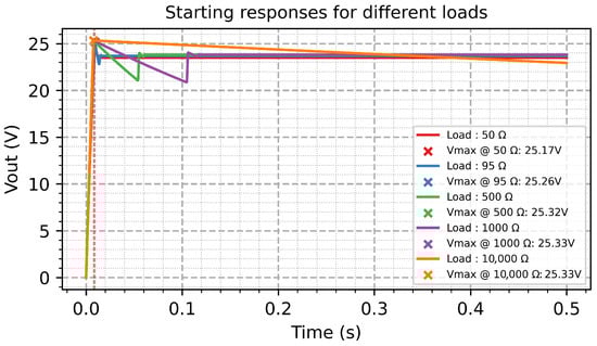
Figure 12.
Start-up voltage responses for different load conditions.
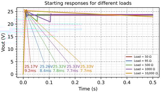
Figure 13.
Measured rise time and peak voltage for each start-up load condition.
For all four cases, which are shown in figures, the rise time and peak voltage are presented. The emulator achieves a steady state in all cases within 10 ms and the result justifies the latency of the Pİ-based controller. Such results are especially promising for applications with fast transients and for those which demand a dependable initialization—like the testing of an MPPT algorithm or real-time controller validation.
5.6. Limitations and Directions for Future Work
Collectively, these results demonstrate that the emulator is capable of replicating PV behavior for which realistic synthetic data could be used under varying conditions. Either working in a static or dynamic way, the system shows a high-precision result and reliable operation quality which facilitate its application for MPPT development, power converter design and laboratorial test. Together with the fast response, model fidelity, and robustness of the emulator, they render it a useful tool for academic as well as industrial purposes.
The simulation shows that the proposed approach achieves a good compromise between advantages of isolated conversion, fast control, and flexibility. There are some add-on features when a two-switch forward is implemented compared to buck or non-isolated topology: enhanced energy transferring efficiency, controlled switching transients, allowable wide range of voltage stress. Additionally, the precision of reproducing PV curves supports trustworthy tests for PV devices and controllers.
These findings confirm the adequacy of the emulator for research, industrial prototyping, as well as educational purposes. The real-time programmability of the spectra and temperature profiles allow a great flexibility in the simulation of diverse solar situations without using any physical PV until we optimize a specific spectral band.
Despite the promising performance demonstrated by the proposed two-switch forward photovoltaic emulator under simulation, several limitations remain at the current stage of development.
First, the validation presented in this study is entirely simulation-based. Although the controller design and topology performance indicate stable and fast-tracking behavior, full experimental validation using the physical prototype has not yet been completed. Hardware non-idealities such as switching delays, parasitic inductances, sensor noise, and electromagnetic interference (EMI) may influence dynamic behavior and will require further investigation through laboratory testing.
Second, the design has been evaluated primarily for low-to-medium laboratory power ranges relevant to MPPT testing and converter validation. Scalability toward higher power levels may necessitate modifications of the transformer design, semiconductor device ratings, thermal management strategies, and EMI suppression techniques.
Third, the temperature-dependent behavior assessed in this work follows user-defined test reference profiles intended for control-performance evaluation. A comprehensive study based on detailed physical parameter identification of real photovoltaic modules and long-duration thermal stress testing will be required to validate the emulator’s performance under realistic temperature dynamics.
Finally, the current PCB layout design has not yet undergone experimental EMI characterization or parasitic parameter measurement, which are crucial for ensuring robust high-frequency operation and regulatory compliance in practical applications.
Future work will, therefore, focus on the following:
Completion of the hardware prototype and full experimental validation, including oscilloscope-based waveform measurements, efficiency testing, and dynamic load response characterization.
EMI measurement and mitigation studies, including parasitic inductance extraction and switching-noise optimization.
Higher-power scalability investigations with enhanced thermal design and device selection strategies.
Advanced control development, such as predictive or adaptive control methods to further improve tracking accuracy under rapidly varying irradiance and temperature profiles.
Integration into hardware-in-the-loop (HIL) platforms for comprehensive testing of MPPT algorithms and grid-interface controllers under realistic operating conditions.
These future developments will enable a complete assessment of the proposed PV emulator architecture and extend its applicability toward real-world testing environments.
6. Conclusions and Future Work
This paper presents the design and modeling of a transformer-isolated photovoltaic emulator based on a two-switch forward-converter topology, validated through simulation. A model-based current reference algorithm with a dual-loop PI control scheme is employed to achieve stable and fast tracking of the desired I–V characteristics under varying irradiance and temperature reference conditions, demonstrating good steady-state regulation and dynamic performance.
The main contribution of this work is the system-level integration of an isolated forward-converter topology with a real-time-oriented control framework for PV emulation, offering galvanic isolation, direct magnetic power transfer, reduced device stress, and flexible load testing capability compared with conventional non-isolated or flyback-based approaches.
Future work will focus on hardware realization and the experimental validation of the proposed PCB prototype, extension toward hardware-in-the-loop (HIL) testing, and the investigation of advanced predictive or adaptive control strategies to further improve tracking accuracy under rapidly changing operating conditions.
Author Contributions
Conceptualization, M.L.; Methodology, M.L. and Y.H.; Validation, M.L., Y.H. and M.T.; Writing—original draft, Y.H.; Writing—review & editing, M.T.; Supervision, Y.H. and M.T. All authors have read and agreed to the published version of the manuscript.
Funding
This research received no external funding.
Data Availability Statement
The data presented in this study are available on request from the corresponding author.
Conflicts of Interest
The authors declare no conflicts of interest.
References
- Lu, D.D.C.; Nguyen, Q.N. A photovoltaic panel emulator using a buck–boost DC/DC converter and a low-cost micro-controller. Sol. Energy 2012, 86, 1477–1484. [Google Scholar] [CrossRef]
- Ramyar, A.; Avestruz, A. Development of a FPGA-Based Photovoltaic Panel Emulator Based on a DC–DC Converter; Technical Report; University of Illinois: Champaign, IL, USA, 2021. [Google Scholar]
- Koutroulis, E.; Kalaitzakis, K.; Tzitzilonis, V. Development of an FPGA-based system for real-time simulation of photovoltaic modules. Microelectron. J. 2008, 39, 1143–1151. [Google Scholar]
- Balakishan, C.H.; Sandeep, N. Development of a microcontroller based PV emulator with current controlled DC–DC buck converter. Int. J. Renew. Energy Res. 2014, 4, 1049–1055. [Google Scholar]
- Azharuddin, S.M.; Babu, T.S.; Bilakanti, N. A near accurate solar PV emulator using dSPACE controller for real-time control. Energy Procedia 2014, 61, 2640–2648. [Google Scholar] [CrossRef]
- Zhang, W. DC–DC Converter Based Photovoltaic Simulator with a Double Current-Mode Controller. Master’s Thesis, Missouri University of Science and Technology, Rolla, MO, USA, 2017. [Google Scholar]
- Dolan, D.S.L.; Durago, J.; Crowfoot, J.; Taufik. Simulation of a photovoltaic emulator. In Proceedings of the North American Power Symposium (NAPS), Arlington, TX, USA, 26–28 September 2010; pp. 1–7. [Google Scholar]
- Yanarates, C.; Zhou, Z. Fast-converging robust PR–P controller designed by using symmetrical pole placement method for current control of interleaved buck converter-based PV emulator. Energy Sci. Eng. 2022, 10, 155–176. [Google Scholar] [CrossRef]
- Yanarates, C.; Zhou, Z. Symmetrical pole placement method-based unity proportional gain resonant and gain scheduled proportional (PR–P) controller with harmonic compensator for single-phase grid-connected PV inverters. IEEE Access 2021, 9, 93165–93181. [Google Scholar] [CrossRef]
- Wang, Y.; Yanarates, C.; Zhou, Z. External current source–based unilluminated PV partial shading emulation system verified through the hybrid global search adaptive P&O MPPT algorithm. Front. Energy Res. 2022, 10, 868951. [Google Scholar]
- Duru, Ö.; Zengin, S.; Boztepe, M. Design and implementation of programmable PV simulator. In Proceedings of the 2016 International Symposium on Fundamentals of Electrical Engineering (ISFEE), Bucharest, Romania, 30 June–2 July 2016; pp. 1–6. [Google Scholar]
- Bautista, O.; Bernal, Á.; Pantoja, A.; Revelo, J. FPGA implementation of a PV generator and boost converter controllers for a virtual laboratory environment. Iran. J. Sci. Technol. Trans. Electr. Eng. 2024, 48, 533–551. [Google Scholar] [CrossRef]
- Choi, S.; Park, S.; Hong, J.; Won, J. A Design and Validation of 400 W PV Emulator Using Simple Equivalent Circuit for PV Power System Test. Energies 2023, 16, 1561. [Google Scholar] [CrossRef]
- del Moral, D.L.; Barrado, A.; Sanz, M.; Lazaro, A.; Zumel, P. Analysis and implementation of the Buck–Boost modified series forward converter applied to photovoltaic systems. arXiv 2024, arXiv:2401.13464. [Google Scholar] [CrossRef]
- Sankar, A.B.; Seyezhai, R. Analysis and development of SiC MOSFET boost converter as solar PV pre-regulator. arXiv 2018, arXiv:1810.11452. [Google Scholar] [CrossRef]
- Kongphet, V.; Migan-Dubois, A.; Delpha, C.; Lechenadec, J.-Y.; Diallo, D. Low-Cost I–V Tracer for PV Fault Diagnosis Using Single-Diode Model Parameters and I–V Curve Characteristics. Energies 2022, 15, 5350. [Google Scholar] [CrossRef]
- Gorecki, K.; Krac, E.; Dabrowski, J. Modelling an influence of solar cells connection manner on PV generator operation with partial shading. Energies 2024, 17, 5741. [Google Scholar] [CrossRef]
- Osorio, L.; Rivera, M.; Tuninetti, V.; Mediaceja, Y.R.; Wheeler, P. A MATLAB/GUI for photovoltaic modules performance simulations based on two-diode model. Preprints 2023. [Google Scholar] [CrossRef]
- El Iysaouy, L.; Bielskis, E.; Lahbabi, M.; Baskys, A.; Oumnad, A. Investigation of microinverter based on the two-switch DC–DC flyback converter topology. IOP Conf. Ser. Earth Environ. Sci. 2018, 161, 012024. [Google Scholar] [CrossRef]
- Rico, J.; Álvarez, M.; Garrido, A. Modified two-switch flyback topology with an active clamp for photovoltaic microinverters. In Proceedings of the 22nd International Conference on Renewable Energies and Power Quality (ICREPQ’24), Bilbao, Spain, 26–28 June 2024. [Google Scholar]
- Iranian, M.E.; Mohseni, M.; Aghili, S.; Parizad, A.; Baghaee, H.R.; Guerrero, J.M. Real-time FPGA-based HIL emulator of power electronics controllers using NI PXI for DFIG studies. IEEE J. Emerg. Sel. Top. Power Electron. 2022, 10, 2005–2019. [Google Scholar] [CrossRef]
- Tan, R.H.G.; Lee, J.S.Z.; Babu, T.S. PV Emulator Model. MATLAB Central File Exchange, 2022. Available online: https://ww2.mathworks.cn/matlabcentral/fileexchange/82853-pv-emulator-model (accessed on 19 November 2025).
- Thakur, H. Improved control strategy for photovoltaic emulator using resistance comparison and binary search method. Energy Procedia 2017, 117, 1067–1074. [Google Scholar]
- Al-Shetwi, S.I.; Al-Abdulkareem, M.S.; Islam, M.S. Hardware-in-the-loop platform for testing photovoltaic system control. Appl. Sci. 2020, 10, 8690. [Google Scholar]
- Salam, A.; Ismail, M.; Amin, M. A comprehensive MATLAB/Simulink PV system simulator with partial shading capability based on two-diode model. Sol. Energy 2011, 85, 2217–2230. [Google Scholar]
- Ritson, S.; Elkhateb, A. An overview of microinverter design characteristics and MPPT control. In Proceedings of the IEEE IEMDC, Toronto, ON, Canada, 15–18 May 2011. [Google Scholar]
Disclaimer/Publisher’s Note: The statements, opinions and data contained in all publications are solely those of the individual author(s) and contributor(s) and not of MDPI and/or the editor(s). MDPI and/or the editor(s) disclaim responsibility for any injury to people or property resulting from any ideas, methods, instructions or products referred to in the content. |
© 2025 by the authors. Licensee MDPI, Basel, Switzerland. This article is an open access article distributed under the terms and conditions of the Creative Commons Attribution (CC BY) license.