Abstract
Transformerless inverters (TIs) are becoming increasingly popular in solar photovoltaic (PV) applications due to their enhanced efficiency and cost-effectiveness. Unlike transformer-based inverters, TIs, which lack transformers and additional components, offer significant advantages in terms of reduced weight, compactness, and lower costs. Research studies have demonstrated that multilevel TIs can achieve lower total harmonic distortion (THD), reduced switching stresses, and higher AC output voltage levels suitable for high voltage applications. However, achieving these outcomes simultaneously with maximum power ratings and the lowest switching frequencies poses a challenge for TI topologies. In light of these challenges, this research proposes the implementation of a 13-level single-source switched-capacitor boost multilevel inverter (SSCBMLI) designed for solar PV systems. The SSCBMLI consists of a single DC power source, switched-capacitor (SC) units, and a full H-bridge. Compared to other existing 13-level multilevel inverter (MLI) configurations, the proposed SSCBMLI utilizes the fewest components to minimize development costs. Moreover, the SSCBMLI offers voltage boosting and can drive high inductive loads, self-voltage-balanced capacitors, an adaptable topology structure, and reliable system performance. Simulations and experimental tests are conducted using PLECS 4.5 and SIMULINK to assess the performance of the proposed SSCBMLI under varying modulation indices, source powers, and loads. A comparative analysis is then conducted to evaluate the SSCBMLI against existing inverter topologies.
1. Introduction
Solar PV energy stands out as one of the most versatile, accessible, and environmentally friendly renewable energy sources for power generation [1]. The initial high cost associated with PV system implementation has steadily decreased thanks to ongoing advancements in manufacturing and deployment techniques. Recognizing the potential for solar PV systems to become the most reliable and cost-effective energy source, several countries, including China, Germany, India, Japan, and the United States, have made substantial investments in deploying these systems for power generation. As of the end of 2020, the cumulative global installed PV capacity reached an estimated 7604 gigawatts direct current (GWdc), with a minimum of 1394 GWdc installed and commissioned in that year, according to the 2021 snapshot of global PV markets by the International Energy Agency-Photovoltaic Power System Program (IEA-PVPS). In the early days of solar PV systems, DC-AC inverters were commonly connected to the grid using transformers as interfaces to provide galvanic isolation and voltage boosting between the input and output sources [2]. However, incorporating transformers in inverters resulted in drawbacks such as increased size, cost, and weight [3]. Moreover, energy conversion efficiency was compromised, making transformers less desirable as power generation technology continued to evolve towards higher efficiency. Consequently, TIs developed without transformers have gained widespread use in PV applications due to their smaller size, lower cost, and reduced weight.
MLIs, also known as TIs with higher AC output voltage levels, have emerged as essential technology for high-power and medium-voltage regulation. Unlike conventional power electronic inverters that provide AC output voltage switching between only two levels, MLIs can generate desired AC output voltages at higher levels using DC voltage sources like fuel cells, capacitors, and renewable energy sources. The concept of MLIs with three levels was first proposed in 1975, and since then, three fundamental MLI technologies have been introduced, including diode-clamped, flying capacitor (FC), and cascaded H-bridge (CHB) topologies. These MLI types produce nearly sinusoidal output waveforms with lower THD, reduced switching losses, and a greater number of AC output voltage levels [4,5]. However, many high-level MLI configurations rely on a high number of input DC voltage sources and passive and active components, resulting in issues such as voltage imbalance, circuit complexity, low operational efficiency, and increased costs. Additionally, improper control algorithm design for switching states often depends on auxiliary circuits to regulate voltage across DC capacitors, further increasing system costs [6]. Furthermore, many MLI topologies lack extensibility in their structure, limiting their ability to handle higher AC output voltage levels and voltage boosting in various applications.
Recently, SC-MLIs have garnered significant attention in power electronics research to address these issues. They offer DC-DC voltage boosting and high-voltage DC-AC inversion capabilities, making them an attractive choice for various applications. Common SC-MLI topologies feature switching circuits with capacitors, diodes, or power switches, enabling them to generate high-level AC output voltage from the DC-link voltage through a series–parallel switching conversion method. This technique allows DC capacitors to charge and discharge at different switching states, with parallel connections to other voltage sources, such as the input DC voltage and other charged capacitors, providing self-voltage regulation—an invaluable solution for many high-power and high-voltage gain applications.
For instance, a SC cascaded half-bridge MLI with a single DC voltage source was proposed in [7]. Unlike conventional CHB-MLIs that require multiple isolated DC voltage sources, this topology uses SC units to replace the DC voltage sources, with a single DC voltage source dedicated to charging the capacitors. It employs four capacitors, four diodes, and ten switches to achieve a nine-level AC output voltage with a four-fold voltage gain from the input DC voltage source. An additional inductor is included to facilitate smooth capacitor charging, limit fault currents, and reduce electromagnetic interference. Comparative studies have shown that this topology offers higher efficiency due to the use of fewer switches.
Another multi-source SC-MLI topology with a K-type module was proposed in [8]. This topology utilizes two asymmetrical DC voltage sources (1DC and 2DC), two capacitors, and 14 switches to generate a 13-level AC output voltage. This asymmetrical MLI module eliminates the need for additional circuits, such as H-bridge, to create a negative AC output voltage level. Furthermore, the topology can be extended by cascading modules in series to achieve higher AC output voltage levels. However, each cascading connection requires an additional set of devices, which may potentially increase the overall system cost. It is worth noting that this topology is limited to a voltage boosting capability of only two times the input DC voltage source.
Similarly to [8], the topology in [9] is another SC-MLI topology with an asymmetrical DC voltage source. This topology uses one capacitor and three switches fewer than the previous one to produce a 13-level AC output voltage, reducing development costs. However, it lacks module extensibility.
The SC-MLI topology in [10] was proposed based on the packed U-cell (PUC) concept, incorporating optimized sliding-mode control to self-balance capacitor voltage in both stand-alone and grid-connected operations. The research paper primarily focuses on presenting a control technique tailored to the proposed topology, addressing the common challenge of capacitor voltage balancing in PUC-based MLIs. It employs only one capacitor, one DC voltage source, and six switches to generate a 7-level AC output voltage. To minimize THD when connecting the topology to the grid, a grid filter is applied. However, it is important to note that while this topology significantly reduces the number of components, it does require an auxiliary control circuit to handle voltage regulation issues across the capacitors. Additionally, it lacks a voltage boosting feature.
This paper introduces a novel SSCBMLI topology, which offers several advantages compared to recent MLI designs. These benefits stem from a reduced number of components, resulting in lower system losses, a smaller inverter size, and reduced cost. The proposed topology relies on a single DC voltage source to generate a 13-level AC output voltage with high gain, simplifying the control algorithm due to the minimal need for gate signals. Additionally, the topology’s DC capacitors possess self-balancing capabilities, eliminating the need for auxiliary circuits to regulate voltage. Furthermore, this proposed topology’s structure is extendable to provide higher AC output voltage levels and voltage boosting. To validate its performance, a comprehensive analysis and verification of the proposed MLI topology were conducted through simulation and hardware implementation.
2. The Proposed SSCBMLI
The circuit structure of the proposed 13-level SSCBMLI topology is shown in Figure 1. This topology consists of 4 key parts: the single-source cell, the SC cell, the extendable unit, and the H-bridge cell. Specifically, it comprises a sole DC voltage source (i.e., Vdc), two diodes (i.e., D1 and D2), three capacitors (i.e., Cu, Cd, and C1), and 11 switches (i.e., comprising one transistor and 10 insulated gate bipolar transistors (IGBTs), each with an anti-parallel diode).
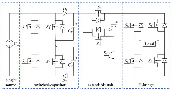
Figure 1.
Circuit structure of the proposed 13-level SSCBMLI.
The H-bridge cell facilitates DC to AC inversion by altering the polarity of the AC output voltage at the load. Its inclusion reduces the number of switches and enhances the extensibility of the SC unit, thereby improving performance. In Figure 1, the SC cell manages the charging and discharging of capacitors (i.e., Cu and Cd) to the DC source voltage Vdc using a parallel connection (i.e., Vcu = Vcd = Vdc). This approach ensures self-voltage balancing across the DC capacitors without requiring an auxiliary voltage-regulation circuit.
2.1. Extensibility of Structure
The extendable unit, depicted in Figure 1, consists of a capacitor, a transistor, and two IGBTs with anti-parallel diodes. To achieve a higher AC output voltage level and greater voltage gain, the extendable unit can be expanded by adding similar units in parallel [11,12]. Figure 2 illustrates an example of the extendable unit structure with n = 1 and n = 2, where the unit is placed between the SC cell and the H-bridge cell.
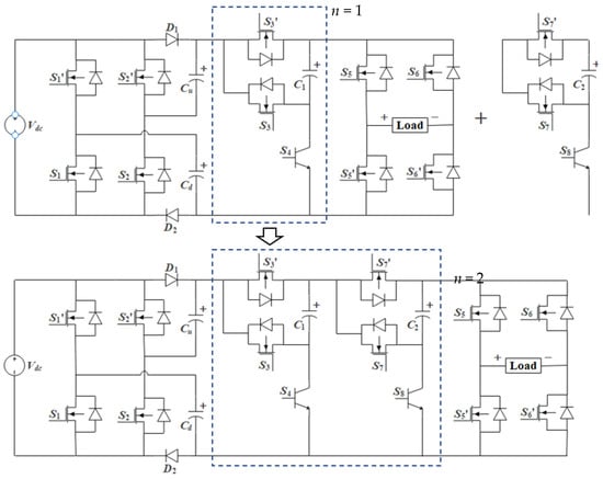
Figure 2.
Extended SC extendable unit structure with n = 1 and n = 2.
The voltage across each additional SC extendable unit capacitor Cn can be controlled to (3)(2n−1)Vdc. For instance, when n = 1, capacitor C1 charges to 3Vdc by summing the DC voltage source and SC cell voltages (i.e., Vc1 = Vdc + Vcu + Vcd). When n = 2 (i.e., with two SC extendable units), capacitor C1 remains charged to 3Vdc, while capacitor C2 charges to 6Vdc by summing the DC voltage source, the SC cell, and the voltage across C1 (i.e., Vc2 = Vdc + Vcu + Vcd + Vc1). A crucial component of the extendable unit is the transistor, which enables parallel conduction with series voltage during capacitor charging.
As the number of SC extendable units Next increases in the proposed SSCBMLI topology, various parameters change, including diode count Ndiode, capacitor count Ncapacitor, gate driver count Ngate, switch count Nswitch, total component count Ncomponent, voltage boost Vboost, and voltage level Nlevel, as summarized in Table 1.

Table 1.
Value change of parameters with SC extendable units.
2.2. Operation, Switching, and Capacitor States
Figure 3 illustrates the detailed circuit operations and conducting paths for achieving voltage levels from 0 to +6Vdc. The red paths indicate capacitor discharging, and green paths represent capacitor charging. The analysis of the proposed model is conducted under ideal and steady-state conditions, assuming the capacitors have sufficient capacitance to maintain a constant voltage. In particular, capacitors Cu and Cd are charged by the DC voltage source Vdc, resulting in potentials Vcu and Vcd equal to Vdc. Capacitor C1, on the other hand, is charged by Vdc, Vcu, and Vcd, leading to a potential Vc1 equal to the sum of Vdc, Vcu, and Vcd, which is equivalent to 3Vdc. During operation, the capacitors discharge to provide discrete voltage levels when connected in series with the load. Conversely, they are charged when connected to the DC voltage source and other capacitors in parallel. This design enables the proposed SSCBMLI topology to amplify the input voltage source by a factor of six, generating a 13-level AC output voltage when n = 1. It is noteworthy that the capacitor voltage control in the SC cell is achieved using the nearest level control (NLC) technique. This method selects the switching states such that the output voltage closely matches the reference waveform. By ensuring that the required voltage level is generated, the NLC inherently balances the capacitor voltages without requiring complex feedback or additional balancing circuits. This simplifies the control strategy while maintaining the desired output voltage waveform and system efficiency.
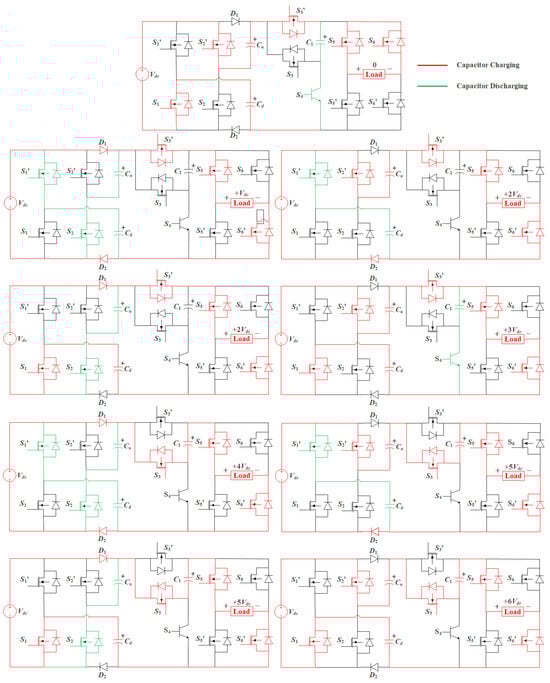
Figure 3.
The operational states of the proposed SSCBMLI at zero and positive voltage levels.
Table 2 summarizes the switching states and capacitor conditions corresponding to each AC output voltage level, which are discussed below:
Table 2.
Switching and capacitor states of the proposed 13-level SSCBMLI topology.
3. Simulation of the Proposed SSCBMLI Topology
3.1. Simulation Specifications
The simulation of the proposed 13-level SSCBMLI was conducted using PLECS 4.5, following the specifications provided in Table 3.
Table 3.
Simulation specifications for the 13-level SSCBMLI.
3.2. Simulation Performance Verification
Figure 4 illustrates the AC output voltage and current produced by the 13-level SSCBMLI when the load transitions abruptly from an R load to an RL load at MI of 1.0. The 13-level SSCBMLI generates 13 discrete levels of AC output voltage and current at a unity MI, achieving a peak output voltage of approximately 600 V—significantly higher than the 100 V input DC voltage. This reflects the topology’s capacity to boost the input DC voltage Vdc, demonstrating a voltage gain of six. The AC output current generated under R and RL loads is also illustrated, with the first five cycles representing the R load response, and subsequent cycles reflecting RL load operation. The AC current waveform transitioning from non-sinusoidal to a stable sinusoidal pattern highlights the topology’s capability to accommodate RL loads effectively.
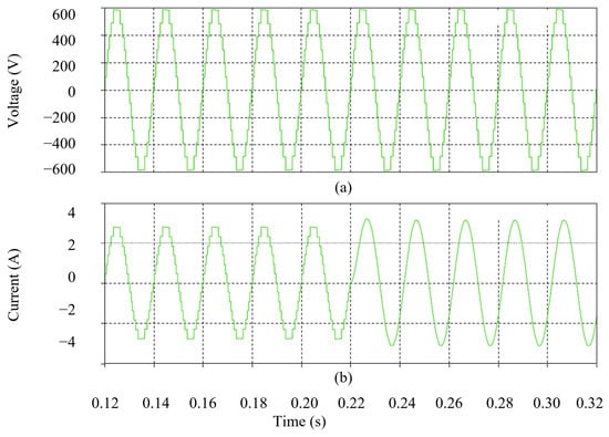
Figure 4.
Simulation results of AC output voltage vout and current iout during R to RL load transition at MI = 1.0.
In Figure 4a, the AC output voltage levels and amplitude remain consistent during the transition from an R load to an RL load, demonstrating the topology’s ability to maintain a stable voltage output regardless of load changes. In Figure 4b, although the AC output current retains the same 13 discrete levels, its amplitude varies as the load shifts to an RL configuration. Under RL loading, the AC output current waveform exhibits a pure sinusoidal shape, further showcasing the topology’s effectiveness in accommodating and stabilizing under RL loads.
Figure 5 shows the waveforms of DC voltage, DC current, and power for capacitors Cu, Cd, and C1, highlighting their charging and discharging behavior. Figure 5a,b show the DC voltage waveforms for capacitors Cu, Cd, and C1, demonstrating their voltage regulation during charging and discharging cycles. Figure 5c presents the DC current waveforms, highlighting the charging and discharging current characteristics of the capacitors. Figure 5d depicts the power waveforms, illustrating the energy transfer and utilization, as well as the charging and discharging power dynamics of Cu, Cd, and C1 within the circuit.
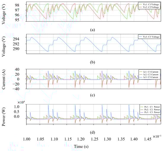
Figure 5.
Simulation results showing voltages (Vcu, Vcd, Vc1), currents (Icu, Icd, Ic1), and powers (Pcu, Pcd, Pc1) for capacitors at MI = 1.0.
The DC voltage across Cu and Cd remains balanced at Vdc = 100 V each, while C1 maintains at a DC voltage of 3Vdc = 300 V. This demonstrates that the capacitors possess inherent self-regulation capabilities, eliminating the need for auxiliary control circuits. During operation, the capacitors cyclically charge and discharge to maintain stable DC voltage levels.
3.3. Total Harmonic Distortion (THD) vs. Modulation Index (MI)
A THD analysis was conducted through simulation to assess power quality under R and RL loads at various MI values, based on AC output voltage and current waveforms captured over five cycles for each load at different MI values. Figure 6 and Table 4 reveal that the R load exhibits greater distortion in the AC current output waveforms than the RL load across different MI values. This higher harmonic content is due to the absence of reactive elements, such as inductance, in the R load circuit. In contrast, an RL load, which includes both resistance and inductance, introduces a filtering effect that dampens higher-frequency harmonics in the current waveform. Inductors resist changes in current, especially at higher frequencies, which helps reduce harmonic distortion, as observed in Table 4.
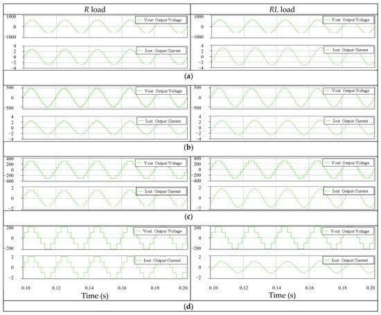
Figure 6.
Simulation results of AC output voltage vout and AC output current iout for MI values: (a) 1.0, (b) 0.8, (c) 0.5, and (d) 0.3 under R load and RL load.
Table 4.
Simulation results of voltage and current THD (%) for R and RL loads with varying MI.
The effects of MI variation on the AC output voltage and current are also notable. As MI decreases from 1.0 to 0.8, 0.5, and 0.3 (at 0.2 s, 0.3 s, 0.4 s, and 0.5 s, respectively), the amplitude of the modulating signal reduces, impacting both the amplitude and shape of the waveforms, as shown in Figure 7. Specifically, lower MI values result in decreased amplitude and potential changes in harmonic content, as summarized in Table 4.
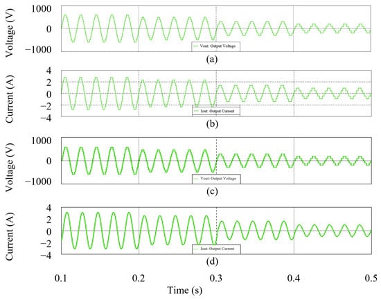
Figure 7.
Transition of AC output voltage vout and current iout for different MI values under R load (a,b) and RL load (c,d).
3.4. Efficiency and Power Loss Analysis
This section examines the efficiency and power dissipation of the proposed 13-level SSCBMLI topology, based on simulation results. To ensure realistic assessment, power components are configured in accordance with the manufacturer specifications. For this analysis, the models C3M0025065K and C3D16060D are used as switches and diodes in the simulation, which is conducted under steady-state conditions with a heat sink at an ambient temperature of 25 °C.
In this analytical framework, the total power loss Ploss,total, includes contributions from conduction losses Pcond and switching losses Psw due to both active and passive switches, as well as resistive losses Pr and ripple losses Prip from capacitors. Consequently, the total power loss and efficiency can be expressed as follows:
Conduction loss refers to heat generated by the switches and diodes during steady-state operation. This loss is calculated by considering the average current and internal resistance of each switch and diode in its on-state. The total conduction loss Pcond,total, can thus be derived as follows:
where Iavg,sw represents the average current through the switch in its on-state, Iavg,d is the average diode current in its on-state, Ron,sw is the switch’s on-state resistance, and Ron,d is the diode’s on-state resistance.
Active switches also exhibit time delays during turn-on and turn-off phases. This delay, along with abrupt switching processes, creates overlaps in voltage and current, which results in switching losses. The total switching loss Psw,total is then derived as follows:
where f represents the operating frequency, Von and Ion are the voltage and current during turn-on, ton is the duration of the turn-on phase, and Voff and Ioff represent voltage and current during turn-off, with toff as the turn-off duration.
Capacitor resistive loss Pr results from power dissipation due to the internal resistance of the capacitors. Capacitor ripple loss Prip, however, arises from voltage fluctuations during charging and discharging cycles. The capacitor resistive and ripple losses are expressed as follows:
where Rc is the capacitor’s internal resistance, Ic,charge and Ic,discharge represent current during charging and discharging, ∆Vc is the voltage drop across the capacitor, fc is the switching frequency, and δ (i.e., set at two) represents the dissipation factor.
Table 5 presents the efficiency and power dissipation characteristics of the proposed 13-level SSCBMLI topology, evaluated under an R load, with source power adjusted across 50 W, 100 W, 200 W, 500 W, and 1000 W by varying resistance values.
Table 5.
Efficiency and power dissipation of the proposed 13-level SSCBMLI topology.
4. Experiment of the Proposed SSCBMLI Topology
4.1. Experiment and Hardware Setup Specifications
The experiment for the proposed 13-level SSCBMLI topology was conducted according to the specifications outlined in Table 6 to validate its practical performance.
Table 6.
Experiment specifications for the proposed 13-level SSCBMLI.
A small-scale prototype was utilized, with a single input DC voltage set at 20 V. The prototype was tested under various MI conditions with both R and RL loads to obtain experimental results. To accommodate the higher charging and discharging rates, the capacitance values of C1 and C2 were chosen to be greater than that of C3. In the experimental setup, the AUIRGP50B60PD1 was employed as an IGBT switch with an anti-parallel diode, while the IGW30N60T functioned as a transistor in S4 of the extendable SC unit.
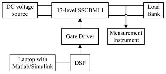
Figure 8.
Block diagram of the simulation setup for the 13-level SSCBMLI.
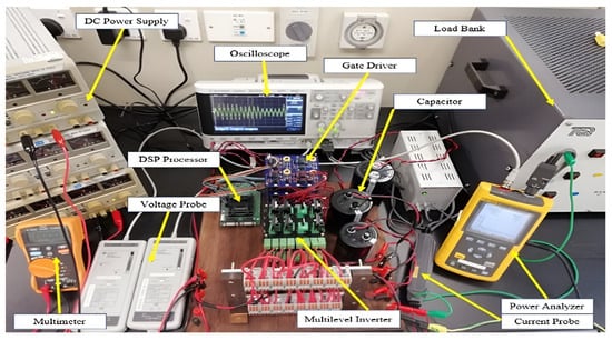
Figure 9.
Experiment setup for the 13-level SSCBMLI.
The Digital Signal Processor (DSP) controller, EZDSP F28335, generated gate signals based on the control algorithm implemented in SIMULINK R2018a. To drive the IGBTs, the gate signals were amplified from 5 V to ±15 V using the optocoupler gate driver HCPL-3120. These amplified signals were then transmitted to the IGBTs for switching. The prototype was powered by DC voltage and connected to a load bank. Voltage and current probes measured the outputs at the load, while an oscilloscope and power analyzer were used to visualize the output values and behaviors for data collection and analysis.
4.2. Experiment Performance Verification
A THD analysis was conducted on the prototype to assess the practical power quality generated by the proposed 13-level SSCBMLI topology. Similar to the simulation phase, the prototype was tested with an R load and an RL load, with MI values of 0.3, 0.5, 0.8, and 1.0. Figure 10 presents the experimental results of AC output voltage Vout and output current Iout, along with power analysis and harmonic profiles for both loads. All figures depict the AC output voltage waveform Vout and AC output current waveform Iout, with scales of 50 V/division and 0.5 A/division, respectively.
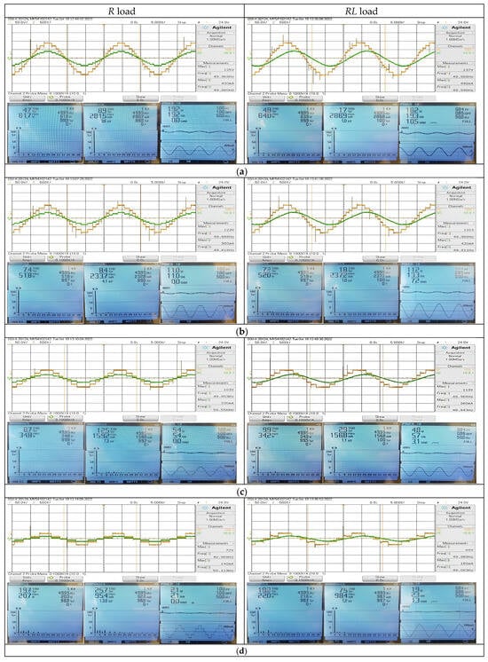
Figure 10.
Experiment results of AC output voltage vout and AC output current iout for MI values: (a) 1.0, (b) 0.8, (c) 0.5, and (d) 0.3 under R load and RL load.
The experimental outcomes for AC output voltage and output current, along with their respective THD values for both R and RL loads under varying MI, are summarized in Table 7.
Table 7.
Experiment results of voltage and current THD (%) for R and RL loads for variation of MI.
The tabulated results indicate that the minimum THD is observed at an MI of 1.0, with approximately 4.7% for the AC output voltage at the R, and 1.7% for the AC output current at RL load. Both voltage and current THD values increase significantly as MI decreases. Although the THD results obtained are considered low for 13-level MLIs, filters are commonly employed to further reduce output THD. Additionally, extending the proposed topology to achieve a higher number of output voltage levels can significantly reduce THD.
Table 8 presents a comparison between the simulation and experimental results for the THD of both the AC output voltage and output current in the proposed 13-level SSCBMLI topology. The analysis is conducted under varying MI values for R and RL loads. The results reveal minor variations between the simulation and experimental measurements. For instance, the experimental AC output voltage THD is 4.7%, slightly lower than the simulation result of 6.41% when the proposed SSCBMLI operates with a purely resistive load at MI = 1.0. These discrepancies are primarily attributed to the limitations of the power analyzer’s precision during the experimental phase. Additional contributing factors include non-ideal switching behavior, measurement noise, and real-world parasitics, which are not accounted for in simulations. Notably, during the experimental phase, the proposed topology demonstrates exceptionally low voltage THD, maintaining values below 5% at MI = 1.0. This result highlights the capability of the proposed topology to generate high-quality output voltage waveforms suitable for practical applications. On the other hand, current THD is more sensitive to variations in MI and load characteristics, with experimental results showing a slight increase compared to simulations, particularly at lower MI values. This difference is likely due to the inherent effects of load dynamics and the interactions between real-world inductive and resistive components. Overall, the comparison consistently validates the performance of the proposed 13-level SSCBMLI topology in both simulation and experimental phases, demonstrating its effectiveness and reliability in achieving low harmonic distortion under various operating conditions.
Table 8.
Comparison between simulation and experiment results of voltage and current THD (%) for R and RL loads for variations of MI.
4.3. Comparative Study
This section presents a comparative study, positioning the proposed 13-level SSCBMLI topology alongside existing 13-level MLI topologies from references [8,9,13,14,15,16,17,18,19,20,21,22,23]. Parameters used to highlight differences among these topologies include Nsource, Ncomponent, Nswitch, Ndiode, Ncapacitor, Ngate, Vboost, and the circuit structure’s extensibility, all detailed in Table 9. As observed, the proposed topology incorporates only one DC voltage source, using the fewest components and gate drivers necessary to generate a 13-level AC output voltage while achieving high voltage boosting and extensibility. In contrast, MLI topologies in references [8,9,18] have fewer components but exhibit a reduced voltage-boosting factor. Other topologies, such as those in references [16,22,23], feature extensible structures with high voltage gain but require a higher component count. Therefore, the proposed topology stands out as the most cost-effective option, requiring fewer components and gate drivers and relying on a single DC voltage source. Furthermore, by extending the circuit structure, higher voltage gains and levels can be achieved with minimal additional components.
Table 9.
Comparison of the proposed 13-level SSCMLI topology with existing 13-level MLI topologies.
This cost advantage is further analyzed in Table 10, which compares the component and gate driver costs of the proposed topology with other SSCBMLIs presented in [13,14,16,17,19,20,21,22,23], all achieving the same voltage boosting gain. Among these designs, the proposed topology demonstrates the lowest component count and an overall cost of USD 87.08, owing to its efficient configuration. In contrast, the referenced topologies achieve the same voltage boosting factor but require more components and gate drivers, leading to a higher overall cost. Consequently, the proposed topology strikes an optimal balance by delivering the same voltage boosting capability with fewer components and gate drivers, making it a cost-effective and practical solution for high-performance applications.
Table 10.
Cost comparison of SSCBMLI with proposed topology for the same voltage gain of six.
5. Conclusions
This research introduces a novel MLI design, specifically a 13-level SSCBMLI topology. The proposed topology efficiently utilizes a single DC voltage source, employing a minimal number of components and gate signals to achieve a 13-level AC output voltage. The topology’s SC unit allows for extensibility, enabling the inverter to produce higher AC output voltage levels, which significantly enhances voltage gain. The series-parallel configuration of DC capacitors provides self-voltage balancing and voltage boosting without the need for additional circuits. With high overall efficiency and reliable performance under RL loads, this topology is well-suited for solar PV applications. Extensive testing, including both simulation and experimental analyses across various loads and MI values, has validated the performance and advantages of the proposed topology. The output THD for the proposed topology is exceptionally low for a 13-level MLI. A comparative study further shows that the proposed SSCBMLI utilizes the fewest components and gate drivers to achieve a 13-level AC output voltage, with a voltage gain six times the input DC voltage source. These advanced characteristics make the proposed 13-level SSCBMLI a feasible and cost-effective choice as a solar inverter, promising high power and voltage potential in future applications.
Author Contributions
Conceptualization, Y.W.S.; methodology, Y.W.S.; software, Y.W.S.; validation, K.H.L., S.P.A. and K.S.K.Y.; formal analysis, Y.W.S.; investigation, Y.W.S.; resources, K.H.L. and R.C.W.C.; Writing—original draft, K.H.L., Y.W.S., S.P.A. and S.Y.S.; writing—review and editing, K.H.L., S.P.A. and S.Y.S.; visualization, K.H.L.; supervision, K.H.L. and R.C.W.C.; project administration, K.H.L.; funding acquisition, K.H.L., S.P.A. and K.S.K.Y. All authors have read and agreed to the published version of the manuscript.
Funding
This research was funded by Universiti Teknologi Brunei (UTB) and the APC was funded by UTB.
Data Availability Statement
The original contributions presented in this study are included in the article. Further inquiries can be directed to the corresponding author.
Acknowledgments
The author would like to thank Universiti Teknologi Brunei (UTB) for funding this research work.
Conflicts of Interest
The authors declare no conflict of interest.
References
- Solangi, K.; Islam, M.; Saidur, R.; Rahim, N.; Fayaz, H. A review on global solar energy policy. Renew. Sustain. Energy Rev. 2011, 15, 2149–2163. [Google Scholar] [CrossRef]
- Carrasco, J.M.; Franquelo, L.G.; Bialasiewicz, J.T.; Galván, E.; PortilloGuisado, R.C.; Prats, M.M.; León, J.I.; Moreno-Alfonso, N. Power-electronic systems for the grid integration of renewable energy sources: A survey. IEEE Trans. Ind. Electron. 2006, 53, 1002–1016. [Google Scholar] [CrossRef]
- Kerekes, T.; Teodorescu, R.; Rodrıguez, P.; Vázquez, G.; Aldabas, E. A new high-efficiency single-phase transformerless PV inverter topology. IEEE Trans. Ind. Electron. 2009, 58, 184–191. [Google Scholar] [CrossRef]
- Suresh, L.P. A brief review on multilevel inverter topologies. In Proceedings of the 2016 International Conference on Circuit, Power and Computing Technologies (ICCPCT), Nagercoil, India, 18–19 March 2016; IEEE: New York, NY, USA, 2016; pp. 1–6. [Google Scholar]
- Koshti, A.K.; Rao, M. A brief review on multilevel inverter topologies. In Proceedings of the 2017 International Conference on Data Management, Analytics and Innovation (ICDMAI), Pune, India, 24–26 February 2017; IEEE: New York, NY, USA, 2017; pp. 187–193. [Google Scholar]
- Rodriguez, J.; Lai, J.-S.; Peng, F.Z. Multilevel inverters: A survey of topologies, controls, and applications. IEEE Trans. Ind. Electron. 2002, 49, 724–738. [Google Scholar] [CrossRef]
- Khoun-Jahan, H.; Shotorbani, A.M.; Abapour, M.; Zare, K.; Hosseini, S.H.; Blaabjerg, F.; Yang, Y. Switched capacitor based cascaded half-bridge multilevel inverter with voltage boosting feature. CPSS Trans. Power Electron. Appl. 2021, 6, 63–73. [Google Scholar] [CrossRef]
- Samadaei, E.; Kaviani, M.; Bertilsson, K. A 13-levels module (k-type) with two DC sources for multilevel inverters. IEEE Trans. Ind. Electron. 2018, 66, 5186–5196. [Google Scholar] [CrossRef]
- Siddique, M.D.; Mekhilef, S.; Sarwar, A.; Alam, A.; Mohamed Shah, N. Dual asymmetrical DC voltage source based switched capacitor boost multilevel inverter topology. IET Power Electron. 2020, 13, 1481–1486. [Google Scholar] [CrossRef]
- Babaie, M.; Sharifzadeh, M.; Kanaan, H.Y.; Al-Haddad, K. Switching-based optimized sliding-mode control for capacitor self-voltage balancing operation of seven-level PUC inverter. IEEE Trans. Ind. Electron. 2020, 68, 3044–3057. [Google Scholar] [CrossRef]
- Sia, Y.W.; Law, K.H.; Gopal, L.; Lim, K.H.; Wong, K.I. A new 2-dimension extendable multisource switched capacitor boost multilevel inverter with reduced components. In Proceedings of the 2021 IEEE International Conference in Power Engineering Application (ICPEA), Selangor, Malaysia, 8–9 March 2021; IEEE: New York, NY, USA, 2021; pp. 192–197. [Google Scholar]
- Sia, Y.W.; Law, K.H.; Gopal, L.; Lim, K.H.; Wong, K.I. A new symmetric and asymmetric step-up switched-capacitor integrated multilevel inverter with self-balanced and inductive load capability. In Proceedings of the 2021 International Conference on Green Energy, Computing and Sustainable Technology (GECOST), Virtual, 7–9 July 2021; IEEE: New York, NY, USA, 2021; pp. 1–5. [Google Scholar]
- Sandeep, N. A 13-level switched-capacitor-based boosting inverter. IEEE Trans. Circuits Syst. II Express Briefs 2020, 68, 998–1002. [Google Scholar] [CrossRef]
- Kim, K.-M.; Han, J.-K.; Moon, G.-W. A high step-up switched-capacitor 13-level inverter with reduced number of switches. IEEE Trans. Power Electron. 2020, 36, 2505–2509. [Google Scholar] [CrossRef]
- Panda, K.P.; Bana, P.R.; Panda, G. A reduced device count single DC hybrid switched-capacitor self-balanced inverter. IEEE Trans. Circuits Syst. II Express Briefs 2020, 68, 978–982. [Google Scholar] [CrossRef]
- Roy, T.; Sadhu, P.K. A step-up multilevel inverter topology using novel switched capacitor converters with reduced components. IEEE Trans. Ind. Electron. 2021, 68, 236–247. [Google Scholar] [CrossRef]
- Panda, K.P.; Bana, P.R.; Panda, G. A switched-capacitor self-balanced high-gain multilevel inverter employing a single DC source. IEEE Trans. Circuits Syst. II Express Briefs 2020, 67, 3192–3196. [Google Scholar] [CrossRef]
- Zeng, J.; Lin, W.; Cen, D.; Liu, J. Novel k-type multilevel inverter with reduced components and self-balance. IEEE J. Emerg. Sel. Top. Power Electron. 2020, 8, 4343–4354. [Google Scholar] [CrossRef]
- Ye, Y.; Chen, S.; Wang, X.; Cheng, K.-W.E. Self-balanced 13-level inverter based on switched capacitor and hybrid PWM algorithm. IEEE Trans. Ind. Electron. 2021, 68, 4827–4837. [Google Scholar] [CrossRef]
- Ye, Y.; Zhang, G.; Wang, X.; Yi, Y.; Cheng, K.W.E. Self-balanced switched-capacitor thirteen-level inverters with reduced capacitors count. IEEE Trans. Ind. Electron. 2022, 69, 1070–1076. [Google Scholar] [CrossRef]
- Anand, V.; Singh, V. A 13-level switched-capacitor multilevel inverter with single DC source. IEEE J. Emerg. Sel. Top. Power Electron. 2022, 10, 1575–1586. [Google Scholar] [CrossRef]
- Ye, Y.; Cheng, K.W.E.; Liu, J.; Ding, K. A step-up switched-capacitor multilevel inverter with self-voltage balancing. IEEE Trans. Ind. Electron. 2014, 61, 6672–6680. [Google Scholar] [CrossRef]
- Taghvaie, A.; Adabi, J.; Rezanejad, M. A self-balanced step-up multilevel inverter based on switched-capacitor structure. IEEE Trans. Power Electron. 2018, 33, 199–209. [Google Scholar] [CrossRef]
Disclaimer/Publisher’s Note: The statements, opinions and data contained in all publications are solely those of the individual author(s) and contributor(s) and not of MDPI and/or the editor(s). MDPI and/or the editor(s) disclaim responsibility for any injury to people or property resulting from any ideas, methods, instructions or products referred to in the content. |
© 2025 by the authors. Licensee MDPI, Basel, Switzerland. This article is an open access article distributed under the terms and conditions of the Creative Commons Attribution (CC BY) license (https://creativecommons.org/licenses/by/4.0/).