Abstract
Smart transformers (STs), which are power electronic-based transformers with control and communication capabilities, facilitate managing future distribution grids with distributed generators (DGs) and battery energy storage systems (BESSs). This paper presents a current-fed quadruple active-bridge (CF-QAB) DC–DC converters-based cascaded H-bridge (CHB) ST architecture in which it is easy to coordinate the system-level power transmission and distribution. Compared with the QAB/DAB + Boost baseline, this topology achieves a reduction of approximately 20% in device count. For the core component of the proposed ST architecture, the operation principles are illustrated and the small-signal model is derived. Based on that, the control system obtained by using the individual channel design method is proposed to decouple the highly coupled LV and BESS DC ports, which significantly simplify the control system structure and design process. The experimental results are shown to validate the effectiveness of the proposed DC–DC converter and associated control system.
1. Introduction
World-wide renewable energy resources (RESs) are growing significantly in recent years, which helps in overcoming environmental concerns and energy crises. As the main forms of RES, lots of wind and photovoltaic (PV) distributed generators (DGs) have been installed. However, the intermittent nature of wind and PV DGs poses serious challenges to the stability and reliability of the electric grid [1,2]. In this regard, battery energy storage systems (BESSs) are commonly used to compensate sudden power variations from the DGs, to store the surplus DG power, and to meet the extra load demands during peak hours [3,4]. A low-cost and high-reliability solution for high-power quality photovoltaic power stations (such as distributed rooftop photovoltaics and microgrids) by incorporating battery/supercapacitor storage and a novel ten-switch inverter is provided in [5]. Figure 1a shows the conventional distribution electric grid with DGs and BESSs, where the low-frequency transformers are used as the energy exchange interfaces between the DGs, BESSs, and the grid.
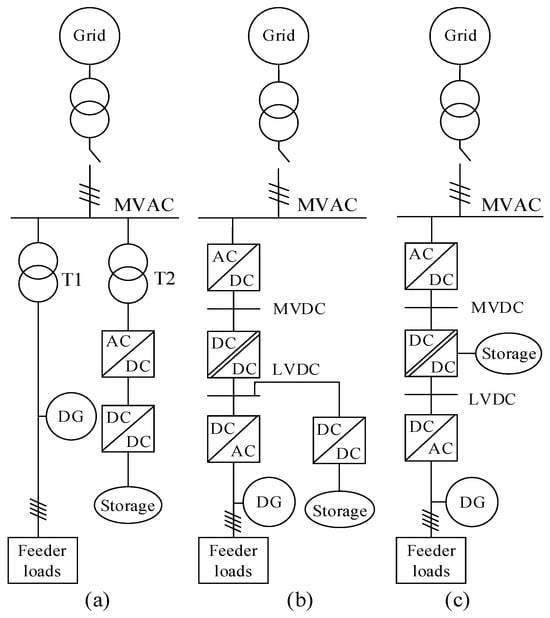
Figure 1.
(a) The conventional distribution electric grid integrated with DGs and BESSs using low-frequency transformers; (b) the distribution electric grid using three-stage STs, where the BESSs are connected to the LV DC-link of the STs; (c) the distribution electric grid using STs integrated with BESSs in the isolated DC–DC stage.
However, the conventional distribution electric grid lacks the power flow control capability and the convenient DC interfaces and therefore cannot meet the operational requirements of future power systems [6]. The smart transformers (STs), which are electronic power-based transformers equipped with effective control and communication features, show high potential to improve the power control and energy management performance of multi-source systems [7,8]. Therefore, combining STs with BESSs can meet the operational and functional requirements of the future distribution electric grids.
Regarding to the ST architectures, numerous works have been reported, which are mainly classified into three categories according to the number of power stages: single-, two- and three-stage STs [9]. Compared with the single- or two-stage architecture, the three-stage ST architecture can not only guarantee power decoupling between the medium voltage (MV) side and low voltage (LV) side but can also offer AC and DC interfaces for various kinds of power sources and loads. Therefore, the three-stage ST architecture is considered as the most suitable candidate for ST implementation and application in the distribution electric grid. References [10,11,12] show several typical three-stage ST architectures, which consist of MV AC–DC rectifiers, isolated DC–DC converters and LV DC–AC inverters. The available converters in the AC–DC stage include NPCs, Cascaded H-bridge (CHB) converters, Modular Multilevel Converters (MMCs), etc. In the isolation stage, there are more options, e.g., dual-active bridge (DAB), single-active bridge (SAB), series resonant converter (SRC), CLLC resonant converter, CF-DAB converter, etc., [13,14,15,16].
Based on the three-stage ST architectures, the BESSs in the distribution electric grid can be connected to the available MV or LV DC-link. Figure 1b shows a typical example, where the BESSs are connected to the LV DC-link of the ST through DC–DC converters. References [17,18] discussed power flow control and energy management in the three-stage ST architectures with the integration of BESSs through the DC-link. However, the above architectures need additional hardware circuits to integrate the BESSs, which increases the system volume and cost. Moreover, the power coordination and cooperation between the STs and BESS converters are necessary, which increases the communication and control system complexity.
In this paper, the architecture of STs integrated with BESSs in the distribution electric grid is presented and shown in Figure 1c, where the typical ST configuration and DC–DC converters are shown in Figure 2 and Figure 3, respectively. Compared with the conventional one in Figure 1b, the architecture in Figure 1c can provide additional DC ports to integrate BESSs in the isolated DC–DC stage, which completely eliminates the need for a specific DC–DC converter for the BESSs. Therefore, the proposed architecture decreases system volume and cost. Additionally, the system-level power flow control and energy management capacity are improved due to centralized control capability. However, for the control system of the DC–DC converter with consideration of the highly coupled relationship between the LV port and the BESS port, the control parameter design in the control system is complicated. Although the system can be divided into several single-input/single-output (SISO) subsystems by using a decoupling matrix, the process of solving the decoupling matrix is complex [19]. Thus, a control system for the DC–DC stage based on an individual channel design method is proposed, which significantly simplifies the structure of the control system. Therefore, the stability and controller parameter tuning can be accurately analyzed by using the Bode and Nyquist diagram techniques of the classical control theory.
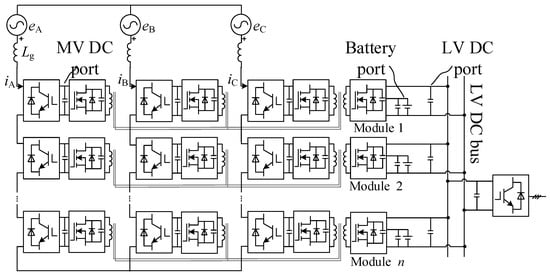
Figure 2.
The proposed CF-QAB-based ST architecture with n modules.
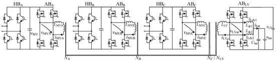
Figure 3.
Detailed circuit of each module, which is composed of three H-bridge cells and one CF-QAB converter.
This paper is organized as follows. In Section 2, the ST architectures are presented, the detailed operation principles are analyzed, and the losses and efficiency are analyzed and compared with other traditional structures. In Section 3, the small-signal models of the DC–DC converters are derived and the control system is designed. The experimental results are presented to verify the effectiveness of the proposed architecture and control system in Section 4. Finally, the conclusions are discussed.
2. Proposed Smart Transformer Architectures
2.1. Topology of the CF-QAB Converters
Figure 2 shows the typical ST architecture. In the AC-DC stage, the cascaded H–bridge (CHB) multilevel converter with n H-bridge cells is adopted. The output voltages of n H-bridge cells in series can synthesize a 2n + 1 level inverter output voltage, which enables the CHB converter available to be directly connected to the medium voltage (MV) grid ej (j ∈ {A, B, C}) through the smoothing inductor Lg. iA, iB, and iC are the three-phase grid currents.
The typical DC–DC stage, which is composed of current-fed quadruple active-bridge (CF-QAB) DC–DC converters, is depicted in Figure 3. Each CF-QAB converter has four AC ports formed by four active bridges, where vMVA, vMVB, vMVC, and vLVac are the AC output voltages of the MV active bridges ABA, ABB, ABC, and the LV active bridge ABLV; LMVA, LMVB, LMVC, and LLV are the inductors connected to corresponding AC ports; iMVA, iMVB, iMVC, and iLV are the windings of the high-frequency transformer NA, NB, NC, and NLV. Additionally, each CF-QAB converter has five DC ports: three MV DC ports connected to the DC-links of H-bridge cells (HBA, HBB, HBC) that respectively belong to phase A, B, and C, one LV DC port connected to the LV DC bus and one battery port connected to the midpoints of the leading leg and lagging leg of the active bridge ABLV through the inductors Lb1 and Lb2. ib1 and ib2 are the currents flowing through the inductors Ldc1 and Ldc2. Cbat and vbat are the battery port capacitor and capacitor voltage. vMV and vLV are the MV and LV DC port voltages, while VMV and VLV are the corresponding port reference voltages.
According to the location relationship between the AC output voltages of the arbitrary MV active bridge ABj and the LV active bridge ABLV, the operation states can be divided into four modes. The corresponding AC output voltage and current waveforms in each mode are depicted in Figure 4, where duty cycle D varies from [0, 1] and DT is equal to min {D, 1 − D}. v’MVj is the output voltage of the active bridge ABj referred to the LV side, which is a three-level AC square wave with duty cycle DT, magnitude V’MVj = VMVNLV/Nj, and phase-shift angle Φj. vLVac is the output voltage of active bridge ABLV with duty cycle DT, magnitude VLV, and phase-shift angle ΦLV. The phase-shift angle ΦjLV is equal to Φj−ΦjLV. ijLV is the current flowing through LLV, which is produced by the active bridge ABj and the LV active bridge ABLV. Practically, the value of D is usually limited within 0.25–0.75 in order to achieve high efficiency, while ΦjLV is usually smaller than π/3 for low circulating loss. Therefore, the CF-QAB converters will mainly operate in mode I and II.
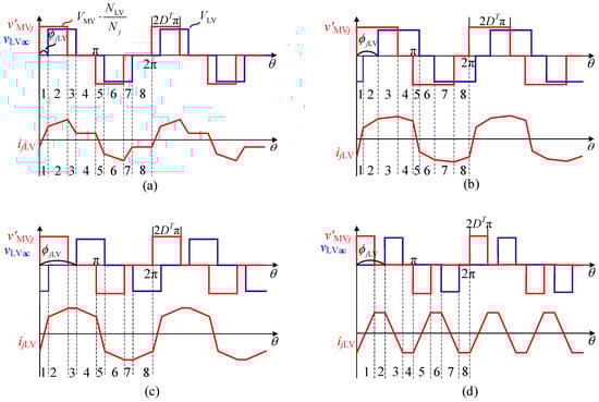
Figure 4.
Output voltage and current waveforms of the arbitrary MV active bridge ABj and the LV active bridge ABLV in four modes (numbers 1–8 represent different time instants): (a) Mode I: Φ < 2πDT and Φ < π − 2πDT; (b) Mode II: Φ < 2πDT and Φ > π − 2πDT; (c) Mode III: Φ > 2πDT and Φ > π − 2πDT; (d) Mode IV: Φ > 2πDT and Φ < π − 2πDT.
The power transmission mechanism can be illustrated by the Y-model circuit of CF-QAB converters in Figure 5a, where Lm and L’MVj are the equivalent magnetizing inductor and the equivalent MV inductor referred to the LV side, respectively. vlLV and vrLV are the voltages of the left and right legs in the LV active bridge ABLV. Here, if the MV active bridge ABj is selected as the sending power port and the LV active bridge ABLV is selected as the receiving power port, then according to Thevenin’s Theorem, the equivalent circuit between ABMVj and ABLV can be obtained as shown in Figure 5b, where LjLV is the corresponding Thevenin-equivalent inductance and v’MVj(th) is the corresponding Thevenin-equivalent voltage with magnitude V’MVj(th). Since the inductor current is periodic and symmetrical over a switching cycle, the initial value of the current flowing through LjLV ijLV(0) can be derived and then the instantaneous inductor current ijLV(θ) over a half switching cycle can be obtained. Finally, the transferred power PjLV from ABj to ABLV can be calculated through the following.
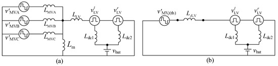
Figure 5.
(a) Equivalent circuit of the CF-QAB converter; (b) equivalent power transmission circuit between ABj and ABLV.
Based on the superposition theorem, the resulting total current flowing through LLV and the total transferred power Ptot into ABLV can be obtained based on the above analysis for single MV active bridge and the LV active bridge. For simplicity, assuming that NA = NB = NC = NLV, LMVA = LMVB = LMVC = LLV = L ≪ Lm, and ΦALV = ΦBLV = ΦCLV = Φ, the total transferred power from MV active bridges to LV active bridges Ptot can be simplified as Ptot_s. The key variables and calculation results in the above analysis are given and summarized in Table 1.

Table 1.
The initial current and transferred power in four modes.
2.2. Comparison and Analysis of Losses and Efficiencies with Other Converters
From the perspective of converter topology, the typical converter topologies (DABs + Boost Converter and QAB + Boost Converter) and the proposed topology (CF-QAB) are shown in Figure 6a–c. Assuming the medium-voltage side voltage is 10 kV, the low-voltage side voltage is 800 V, and the total transmission power is 450 kW, the three different converter topologies mentioned above are adopted as sub-modules. The input voltage of each sub-module port is 800 V. Each sub-module is designed to have a transmission power of 90 kW. The input ports of the module are connected in series and linked to the medium-voltage side voltage through a cascade H-bridge (CHB) structure, and the device selection is as shown in Table 2.
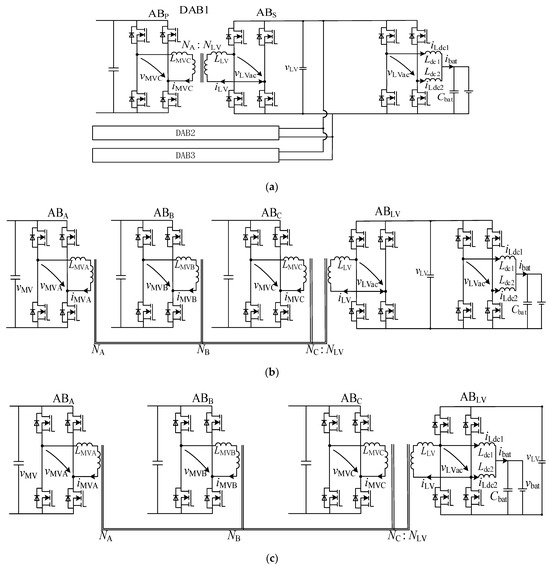
Figure 6.
(a) DAB + Boost Converter for smart transformers with integrated battery energy storage systems. (b) QAB + Boost Converter for smart transformers with integrated battery energy storage systems. (c) CF-QAB converter for smart transformers with integrated battery energy storage systems.
Table 2.
The main devices of different converters (“*” indicates the quantity of devices).
From the topological structure and the above table, it can be seen that the converter proposed in this paper reduces the number of switching tubes compared with the other two converters. Compared with the DAB + Boost converter, it reduces the number of transformers and decreases the size, cost, and volume of the converter. Next, the losses of the three types of converters will be calculated, respectively. The losses of the converters mainly consist of the losses of the switching devices and the losses of the transformers and the inductive components. The losses of the switching devices include on-state losses, turn-on losses, and turn-off losses. The calculation formulas are, respectively, shown as (2) and (3). The losses of transformers and inductive components include winding copper loss and core loss. The calculation formulas are as shown in (4). Since all three converters can achieve MOSFET ZVS (Zero Voltage Switching) turn-on, there is no turn-on loss. The values of other actual parameters needed for reproduction, such as Id_off, tf, and Steinmetz coefficients, can be found in Appendix B Table A1.
CD represents the output capacitance of the switch, Ion represents the current at the switch turn-on time, Ioff represents the current at the switch turn-off time, Id_on represents the turn-on delay time, Id_off represents the turn-off delay time, tr represents the rise time, tf represents the fall time, and VD represents the voltage value after the switch is turned off.
Irms represents the RMS value of the current flowing through the switch. Ron represents on-resistance.
Im_rms represents the RMS current flowing through the magnetic element, Rm corresponds to the AC impedance in the magnetic element. k, α, and β are Steinmentz coefficients, BT represents the maximum change in magnetic induction, and Ve represents the volume of the magnetic component.
The losses of the three converters are shown in Figure 7. The efficiencies of the DAB + BOOST converter, the QAB + BOOST converter, and the CF-QAB converter are 97.56%, 98.09%, and 98.12%, respectively. It can be seen that the converter loss proposed in this paper is lower than that of the DAB + BOOST converter and the QAB + BOOST converter and the efficiency has been improved. Compared with the DAB + BOOST converter, the converter proposed in this paper mainly benefits from the reduction in the number of switching devices and transformers, resulting in significant improvements in losses and efficiency. Compared with the QAB + BOOST converter, the converter proposed in this paper mainly benefits from the reuse of the bridge arms, reducing the number of switching devices, and, by using PWM and phase-shifting techniques, reducing losses and improving efficiency.
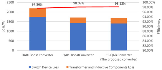
Figure 7.
The losses of different converters.
To further illustrate the advantages of the proposed CF-QAB converter, a Table 3 is provided below, comparing its topological features with those of related converters in terms of structural configuration, BESS integration capability, control complexity, hardware requirements, and system-level advantages.
Table 3.
Comparison of topological features for CF-QAB converter and related converters.
3. Modeling and Control System Design
3.1. Small-Signal Model of the CF-QAB Converters
The corresponding average equivalent circuit model of the CF-QAB converter is depicted as Figure 8, where IQAB is the equivalent average current from the MV side to the LV side. ILdc is the sum of Boost inductor average currents ILdc1, ILdc2. Ldc = 0.5 Ldc1 = 0.5 Ldc2 is the equivalent inductance of parallel Boost inductors Ldc1 and Ldc2. Rdc = 0.5 Rdc1 = 0.5 Rdc2 is the equivalent resistance of parallel inductors Ldc1 and Ldc2. RLV is the equivalent LV side port load. Considering the forward power flow, the battery port can be equivalent to a resistor Rbat. Based on the developed average equivalent circuit model in Figure 6, the average and the small-signal models can be derived. The small-signal state-space equations in main operation modes are derived in Appendix A Equations (A1)–(A4). Accordingly, the transfer functions G11(s), G12(s), G21(s), and G22(s), which represent the relationship between vbat-d, vbat-Φ, vLV-d, and vLV-Φ, are summarized in Equations (5)–(7).
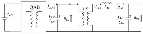
Figure 8.
Average equivalent circuit model of the CF-QAB converters.
Different from the design case in Section 2.2, the specific parameters in the lab/HIL case are shown in Table 4. The Bode plots of the transfer functions G11(s), G12(s), G21(s), and G22(s) can be obtained and compared with circuit simulation results, as shown in Figure 9. It can be seen that the analytical small-signal model is in agreement with the circuit simulation results, which indicates the good accuracy of the established model.
Table 4.
The main parameters of the CF-QAB converter.
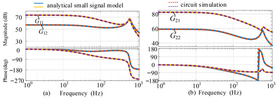
Figure 9.
Bode plots of the proposed converter model: (a) analytical small signal model (b) circuit simulation.
Mode I:
Mode II:
3.2. Control System Design of the CF-QAB Converter
According to the small-signal model of the CF-QAB converter, it can be seen that the converter is a multiple-input and multiple-output (MIMO) system. The corresponding control block diagram is shown in Figure 10, where the PI controllers Gc1 and Gc2 are used for voltage control of the LV side voltage vLV and BESS port voltage vbat of the CF-QAB converter, respectively. Gd(s) represents the delay caused by the sensors, digital controller, and driving circuits, with a delay time of approximately (1–1.5) Ts. In the process of model analysis, the delay function can be approximated as a third order transfer function.
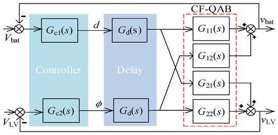
Figure 10.
Control system of the CF-QAB converter.
For the convenience of designing the proposed system controllers and analyzing its stability, the control system based on individual channel design method is proposed in this paper. Based on the small-signal model and the control structure in Figure 10, the MIMO system can be equivalent to two single-input single-output (SISO) systems, as shown in Figure 11. It is worth noting that in the derivation of a single channel, no variable information is lost. Therefore, the stability of the MIMO system in Figure 10 depends on the stability of the two individual SISO systems in Figure 11.
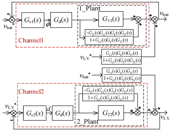
Figure 11.
Equivalent SISO control systems (“*” denotes reference values).
The open-loop gains of single channels are represented as follows:
where γ(s), H1(s), and H2(s) are given in (7)–(9). γ(s) is the Multivariable Information Structure Function (MSF) [20] and its magnitude reflects the coupling degree of the system. The larger the magnitude, the stronger the coupling. Figure 12 shows the Bode plot of γ(s), when the frequency is less than 70 Hz and the amplitude of γ(s) is smaller than 10 dB, indicating that the degree of coupling in the system is small.
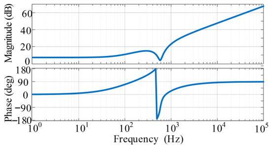
Figure 12.
Bode plot of γ(s).
Based on the equivalent SISO control system and the control system design by using the classical Bode diagram, the Bode plots of T1(s) and T2(s) with blue and red can be obtained as shown in Figure 13. It can be seen that the bandwidths of T1(s) and T2(s) are 3.37 Hz and 30 Hz, respectively, where both of them are less than 70 Hz. The phase margins are 99.5° and 109°, and the corresponding crossover frequencies ωc are 726 Hz and 3770 Hz, respectively, with corresponding gain margins of 21.5 dB and 37.7 dB. Additionally, the closed-loop pole-zero diagrams of T1(s) and T2(s) have been created to further complement the analysis, as shown in Figure 14. Based on the stability criteri-on, it can be concluded that the system is stable.
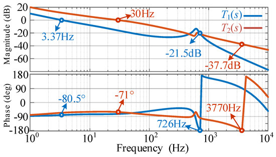
Figure 13.
Bode plots of T1(s) and T2(s).
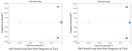
Figure 14.
Closed-loop zero-pole diagrams of T1(s) and T2(s).
4. Experimental Results
To validate the proposed topology and control system, the CF-QAB converter was modeled in Typhoon HIL 402 with the parameters of the power stage provided in Table 2. The rated battery voltage is 200 V, while the three MV-side port voltages are 400 V and the rated LV-side port voltage is 400 V. The turns ratio of the high-frequency transformer is equal to k = 1. Meanwhile, the ADC samplings, the PWM generation, and digital controls are implemented in the DSP 2808 controller. The ADC sampling rate is consistent with the switching frequency, both being 10 kHz. The total measured control-loop delay is one sampling period. The overall experimental setup in the laboratory is shown in Figure 15.
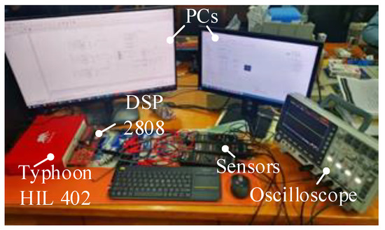
Figure 15.
Experimental setup in the laboratory. (Hardware in the loop).
The experimental results of the CF-QAB converter are presented in Figure 16, Figure 17 and Figure 18. Figure 16a,b show the BESS and LV-side port voltages, and the BESS voltage and current, respectively, before and after t = tstep. The low-voltage (LV) side port voltage (vlv) exhibits remarkable stability. Operating at the rated reference voltage of 400 V, vlv maintains a constant value without significant fluctuations even when the battery energy storage system (BESS) port undergoes dynamic transitions—specifically, when the BESS port voltage steps from 140 V to 160 V and the BESS current steps from 4 A to 6 A. The power absorbed by the LV-side port (PLV) remains constant at 4000 W due to the proposed “individual channel design method,” which decouples the CF-QAB’s MIMO system into two independent SISO subsystems. Combined with PI controllers and precise small-signal parameter design (bandwidth 3.37 Hz, phase margin 99.5°), this strategy ensures stable LV-side voltage regulation. As shown in Figure 16c, Pbat increases from 560 W to 960 W, while PLV stays at 4000 W. Consequently, the total transfer power Ptot = PLV + Pbat rises from 4560 W to 4960 W after t = tstep.
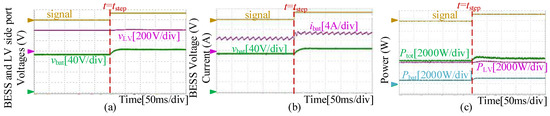
Figure 16.
The dynamic experimental waveforms of the CF-QAB converters when the BESS voltage steps from 140 V to 160 V and the BESS current steps from 4 A to 6 A at t = tstep. (a) The BESS and LV side port voltages vbat and vLV; (b) the BESS voltage and current vbat and ibat; (c) the BESS and LV-side port power Pbat, PLV, and Ptot.
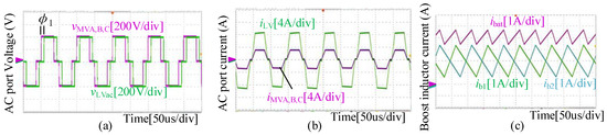
Figure 17.
The experimental waveforms of the CF-QAB converters with the operating point (vbat, ibat) = (140 V, 4 A). (a) The AC output voltages of the MV active bridges and the LV active bridge vMVA, vMVB, vMVC, and vLVac; (b) the inductor currents in the AC ports iMVA, iMVB, iMVC, and iLV; (c) the currents flowing through the BESS port inductors ib1 and ib2, and the BESS port current ibat.
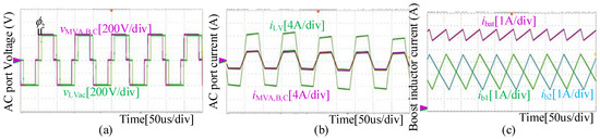
Figure 18.
The experimental waveforms of the CF-QAB converters with the operating point (vbat, ibat) = (160 V, 6 A). (a) The AC output voltages of the MV active bridges and the LV active bridge vMVA, vMVB, vMVC, and vLVac; (b) the inductor currents in the AC ports iMVA, iMVB, iMVC, and iLV; (c) the currents flowing through the BESS port inductors ib1 and ib2, and the BESS port current ibat.
Figure 17 shows the AC output voltages and the inductor currents of the MV and LV active bridges, and the BESS port currents before the step time tstep. In Figure 17a, the AC output voltages of the active bridges are three-level and there is a phase-shift angle φ1 between the MV and LV sides for the power transmission, which is consistent with the analysis of Section 2. In Figure 17b, due to VMV = VLV, the inductor currents are also three-level according to the theoretical analysis. Moreover, the AC inductor current of active bridge ABLV is the sum of the MV side currents iMVA, iMVB, and iMVB.
Figure 17c shows the current flowing into the BESS ibat and the current flowing through BESS port inductors ib1 and ib2. It can be seen that the average value of ibat is 4 A while those of ib1 and ib2 are 2 A. Since the leading leg and lagging leg are phase-shifted with π in the LV active bridge, the ripple of ibat is smaller than that of ib1 and ib2.
Figure 18 shows the AC output voltages and the inductor currents of the MV and LV active bridges, and the BESS port currents after the step time tstep. Similarly, the AC output voltages of the active bridges are three-level and there is a phase-shift angle φ2 between the MV and LV sides as shown in Figure 18a. Due to the increase in duty cycle D for the regulation of BESS voltage, the inductor currents iMVA, iMVB, iMVC, and iLV are nearly two-level, which are the obvious differences with Figure 18b. Figure 17c shows the current flowing into the BESS ibat and the current flowing through BESS port inductors ib1 and ib2. It can be seen that the average value of ibat is 6 A, while those of ib1 and ib2 are 3 A. Therefore, the duty cycle is close to 0.5 and the ripple of ibat is smaller than that in Figure 17c.
5. Conclusions
This paper proposed a current-fed quadruple active-bridge DC–DC converter and the corresponding control system design method for smart transformers with integration of BESSs. The principles of operation, modeling, and control system design based on an individual channel design method were analyzed and the experimental results were shown to validate the analysis. Due to requiring no additional hardware circuits for the BESSs and it being easy to achieve power distribution control, the proposed architecture can not only reduce the system volume and cost but can also improve the system management capability. However, how to achieve an optimized power distribution among the grid, the BESSs, and the load, although it is challenging, has not yet been discussed in detail, so it should be an emphasis of future research.
Author Contributions
Methodology, K.W., Y.Q., Y.Y. and W.T.; Software, Y.Q. and W.T.; Validation, Z.S. and Y.Q.; Formal analysis, K.W., Z.S., Y.Q., Y.Y. and W.T.; Writing—original draft, K.W., Z.S. and Y.Q.; Writing—review & editing, K.W.; Funding acquisition, K.W. All authors have read and agreed to the published version of the manuscript.
Funding
This work was supported by the National Natural Science Foundation of China under Grant 52307215, and in part by Shanghai 2022 Science and Technology Innovation Action Plan-Star Cultivation (Sailing Program) under Grant 22YF1415700.
Data Availability Statement
The original contributions presented in the study are included in the article, further inquiries can be directed to the corresponding author.
Conflicts of Interest
Author Yixian Qu was employed by the company Sungrow Co. Author Wei Tan was employed by the company Shanghai Hanxiang Intelligent Technology Co., Ltd. The remaining authors declare that the research was conducted in the absence of any commercial or financial relationships that could be construed as a potential conflict of interest.
Appendix A
Appendix A.1
Appendix A.2
Appendix A.3
Appendix A.4
Appendix B
Table A1.
Comparison of Key Parameters for Different Converters.
Table A1.
Comparison of Key Parameters for Different Converters.
| DAB + Boost Converter | QAB + Boost Converter | CF-QAB Converter (The Proposed Converter) | |
|---|---|---|---|
| Irms | 32.27 A | 33.5 A(MAB)/102.1 A(LAB) | 30.11 A(MAB)/87.66 A, 93.74 A(LAB) |
| Id_off | 50.04 A | 50.04 A(MAB)/54.37 A(LAB) | 52.38 A(MAB)/143.71 A, 152.09 A(LAB) |
| tf | 38 ns | 75 ns | 78 ns |
| Steinmetz k | 46.208 | 46.208 | 46.208 |
| Steinmetz α | 1.226 | 1.226 | 1.226 |
| Steinmetz β | 3.256 | 3.256 | 3.256 |
| core volume Vcore | 571,400 mm3 | 571,400 mm3 | 571,400 mm3 |
References
- Haegel, N.M.; Kurtz, S.R. Global Progress Toward Renewable Electricity: Tracking the Role of Solar. IEEE J. Photovolt. 2021, 11, 1335–1342. [Google Scholar] [CrossRef]
- Tang, Z.; Yang, Y.; Blaabjerg, F. Power electronics: The enabling technology for renewable energy integration. CSEE J. Power Energy Syst. 2022, 8, 39–52. [Google Scholar] [CrossRef]
- Calero, F.; Cañizares, C.A.; Bhattacharya, K.; Anierobi, C.; Calero, I.; de Souza, M.F.Z.; Farrokhabadi, M.; Guzman, N.S.; Mendieta, W.; Peralta, D.; et al. A Review of Modeling and Applications of Energy Storage Systems in Power Grids. Proc. IEEE 2023, 111, 806–831. [Google Scholar] [CrossRef]
- Suboh, S.M.; Sharma, R.; Tushar, W.; Ahamad, N.B. Enhancing Active Power Dispatchability of WTG-BESS Through Integrated Control Considering Wind Forecast Error. IEEE Access 2024, 12, 2778–2792. [Google Scholar] [CrossRef]
- Tawfiq, K.B.; Zeineldin, H.; Al-Durra, A.; El-Sadaany, E.F. Enhancing photovoltaic grid integration with hybrid energy storage and a novel three-phase ten-switch inverter for superior power quality. Int. J. Electr. Power Energy Syst. 2025, 167, 110580. [Google Scholar] [CrossRef]
- Mandal, A.; Muttaqi, K.M.; Islam, M.R.; Sutanto, D. Solid-State Power Substations for Future Power Grids. IEEE Trans. Ind. Appl. 2025, 61, 1055–1067. [Google Scholar] [CrossRef]
- Bravo, P.; Pereda, J.; Merlin, M.M.C.; Neira, S.; Green, T.C.; Rojas, F. Modular Multilevel Matrix Converter as Solid State Transformer for Medium and High Voltage AC Substations. IEEE Trans. Power Deliv. 2022, 37, 5033–5043. [Google Scholar] [CrossRef]
- Buticchi, G.; Lam, C.-S.; Xinbo, R.; Liserre, M.; Barater, D.; Benbouzid, M.; Gomis-Bellmunt, O.; Ramos-Paja, C.A.; Kumar, C.; Zhu, R. The Role of Renewable Energy System in Reshaping the Electrical Grid Scenario. IEEE Open J. Ind. Electron. Soc. 2021, 2, 451–468. [Google Scholar] [CrossRef]
- Zhu, R.; Liserre, M. Architecture and Topology Overview of Modular Smart Solid-State Transformer. In Proceedings of the 2021 6th IEEE Workshop on the Electronic Grid (eGRID), New Orleans, LA, USA, 5 January 2021; pp. 1–5. [Google Scholar] [CrossRef]
- Wang, K.; Zhu, L.; Wu, W.; Ko, Y.; Zhu, R. Cascaded H-bridge Converter-based Large-Scale Photovoltaic Systems: Power Imbalance and Topology Derivation. In Proceedings of the 2021 IEEE 12th Energy Conversion Congress & Exposition-Asia (ECCE-Asia), Singapore, 13 July 2021; pp. 730–735. [Google Scholar] [CrossRef]
- Ma, D.; Chen, W.; Shu, L.; Qu, X.; Zhan, X.; Liu, Z. A Multiport Power Electronic Transformer Based on Modular Multilevel Converter and Mixed-Frequency Modulation. IEEE Trans. Circuits Syst. II Express Briefs 2020, 67, 1284–1288. [Google Scholar] [CrossRef]
- Huber, J.E.; Kolar, J.W. Applicability of Solid-State Transformers in Today’s and Future Distribution Grids. IEEE Trans. Smart Grid 2019, 10, 317–326. [Google Scholar] [CrossRef]
- Wei, R.; Wang, H.; Kish, G.J.; Li, Y. A Simplified Time-Domain Model-Based Maximum Efficiency Tracking-Aided Synchronous Rectification Strategy for CLLC Chargers. IEEE Trans. Power Electron. 2025, 40, 17160–17171. [Google Scholar] [CrossRef]
- Zhu, R.; Hoffmann, F.; Vázquez, N.; Wang, K.; Liserre, M. Asymmetrical Bidirectional DC–DC Converter with Limited Reverse Power Rating in Smart Transformer. IEEE Trans. Power Electron. 2020, 35, 6895–6905. [Google Scholar] [CrossRef]
- Wang, K.; Zhu, R.; Wei, C.; Liu, F.; Wu, X.; Liserre, M. Cascaded Multilevel Converter Topology for Large-Scale Photovoltaic System with Balanced Operation. IEEE Trans. Ind. Electron. 2019, 66, 7694–7705. [Google Scholar] [CrossRef]
- Guo, J.; Wang, H.; Xu, G.; Sun, Y.; Su, M. Magnetic Integration with Controllable Leakage Inductance and Unbalanced Current Suppression for CF DAB Converter Based on Single EE Core. IEEE Trans. Power Electron. 2025, 40, 15562–15571. [Google Scholar] [CrossRef]
- Marei, M.I.; Alajmi, B.N.; Abdelsalam, I.; Ahmed, N.A. An Integrated Topology of Three-Port DC-DC Converter for PV-Battery Power Systems. IEEE Open J. Ind. Electron. Soc. 2022, 3, 409–419. [Google Scholar] [CrossRef]
- Alajmi, B.N.; Abdelsalam, I.; Marei, M.I.; Ahmed, N.A. Two Stage single-phase EV On-Board Charger Based on Interleaved Cascaded Non-Inverting Buck-Boost Converter. In Proceedings of the 2023 IEEE Conference on Power Electronics and Renewable Energy (CPERE), Luxor, Egypt, 11 May 2023; pp. 1–6. [Google Scholar] [CrossRef]
- Liao, J.; Guo, C.; He, D.; Zhou, N.; Wang, Q.; Wang, Y. Decoupling Control of Triple Active Bridge-Power Flow Controller in Meshed Bipolar DC Distribution Grids. IEEE J. Emerg. Sel. Top. Power Electron. 2022, 10, 7569–7580. [Google Scholar] [CrossRef]
- Ugalde-Loo, C.E.; Acha, E.; Licéaga-Castro, E. Analysis of the damping characteristics of two power electronics-based devices using ‘individual channel analysis and design’. Appl. Math. Model. 2018, 59, 527–545. [Google Scholar] [CrossRef]
Disclaimer/Publisher’s Note: The statements, opinions and data contained in all publications are solely those of the individual author(s) and contributor(s) and not of MDPI and/or the editor(s). MDPI and/or the editor(s) disclaim responsibility for any injury to people or property resulting from any ideas, methods, instructions or products referred to in the content. |
© 2025 by the authors. Licensee MDPI, Basel, Switzerland. This article is an open access article distributed under the terms and conditions of the Creative Commons Attribution (CC BY) license (https://creativecommons.org/licenses/by/4.0/).