Abstract
In recent years, the trend in power electronics has been toward high-efficiency and high-power-density converters. Additionally, this trend has allowed electric vehicles to accommodate larger batteries, which necessitate bi-directional capabilities not only for driving but also for vehicle to grid (V2G), etc. This article proposes a comparative analysis of GaN-based bi-directional topologies, namely the dual active bridge (DAB) converter and the CLLC converter. To ensure a fair analysis of the proposed topologies, prototypes with the same target of efficiency above 97.5% and a power density of 5.5 kW/L have been constructed. This research can support the adoption of 10.9 kW bi-directional topologies in GaN-based on-board chargers (OBCs) for EVs.
1. Introduction
Major agreements such as the Paris Agreement and COP 28 have been signed to solve the problem of climate change caused by carbon and greenhouse gas (GHG) emissions [1,2,3,4,5,6,7,8,9,10,11,12,13]. In particular, the road transportation sector is highly dependent on fossil fuels and accounts for about 77% of global transport-related GHG emissions [6]. For this reason, the Inland Transportation Commission (ITC) of UNECE recommended the adoption of EVs [5,6], so the demand for EVs is increasing [4]. In addition, the high efficiency and high power density of the EVs’ power conversion system are important to reduce energy consumption [9,10,11,12,13,14,15,16,17,18,19,20,21,22,23,24,25,26,27,28,29]. High efficiency can reduce energy loss in the process of transmitting power and increase the stability of the system through less heat generation. Also, since EVs are equipped with batteries, high power density is required due to spatial limitations.
Several studies have been carried out on on-board chargers (OBCs) [14,15,16,17,18,19,20,21,22,23,24,25], but they focus on unidirectional power conversion. Recently, OBCs were adopted with a bi-directional topology, such as vehicle to grid (V2G) and vehicle to load (V2L), to use energy efficiently. Representative bi-directional topologies are dual active bridge (DAB) and CLLC converters. These topologies have the advantages of wide input/output voltage range and low voltage stress, so they are widely adopted in OBCs.
In [26], a 3.3 kW/500 kHz DAB was proposed as the OBC DC-DC stage. It was designed as follows to satisfy the requirements of a high efficiency and high power density:
- Bare-Die SiC MOSFETs of 4 mm × 6 mm size were applied instead of a conventional packaged switch. The developed switch module has low switching loss and low oscillations due to its low parasitic composition, which can operate at high frequency.
- The volume was reduced by using the leakage inductance of a planar transformer without using an additional inductor. Zero voltage switching (ZVS) was achieved in the battery voltage range of 250–380 V, and the final prototype had a power density of 5.44 kW/L. Using a DAB, up to 98% efficiency was satisfied in the constant power (CP) section.
In [28], bi-directional power conversion was reviewed by applying CLLC. In order to increase the efficiency and power density, the following proposal was made:
- Loss reduction was produced through soft switching and synchronous rectification (SR). Through SR driving, the efficiency increased by up to 1.7%.
- An integrated transformer using leakage inductance was proposed. As a result, efficiencies of 97.5% and 97.3% were satisfied in grid to vehicle (G2V) and V2G.
In [30], a 1 kW OBC system using SiC MOSFETs was implemented with both a DAB and CLLC designed as a full-bridge and half-bridge, respectively. However, additional inductors were designed without the transformer’s leakage inductance.
The abovementioned articles have been studied on only one topology or comparing two topologies without the same constraints such as high power density. In addition, the design directions for each conventional topology have not been compared and presented. Therefore, this article proposes a comparative analysis of typical DAB and CLLC converters in charging mode at 5.5 kW/L and, 10.9 kW using the transformer’s leakage inductance. Section 2 provides a theoretical analysis of the conventional DAB and CLLC converters. Section 3 discusses the design direction of each topology and each transformer. The experimental results and an analysis of the experimental results are provided in Section 4 and Section 5, respectively. Finally, Section 6 provides the conclusion of this article.
2. Operation Principles
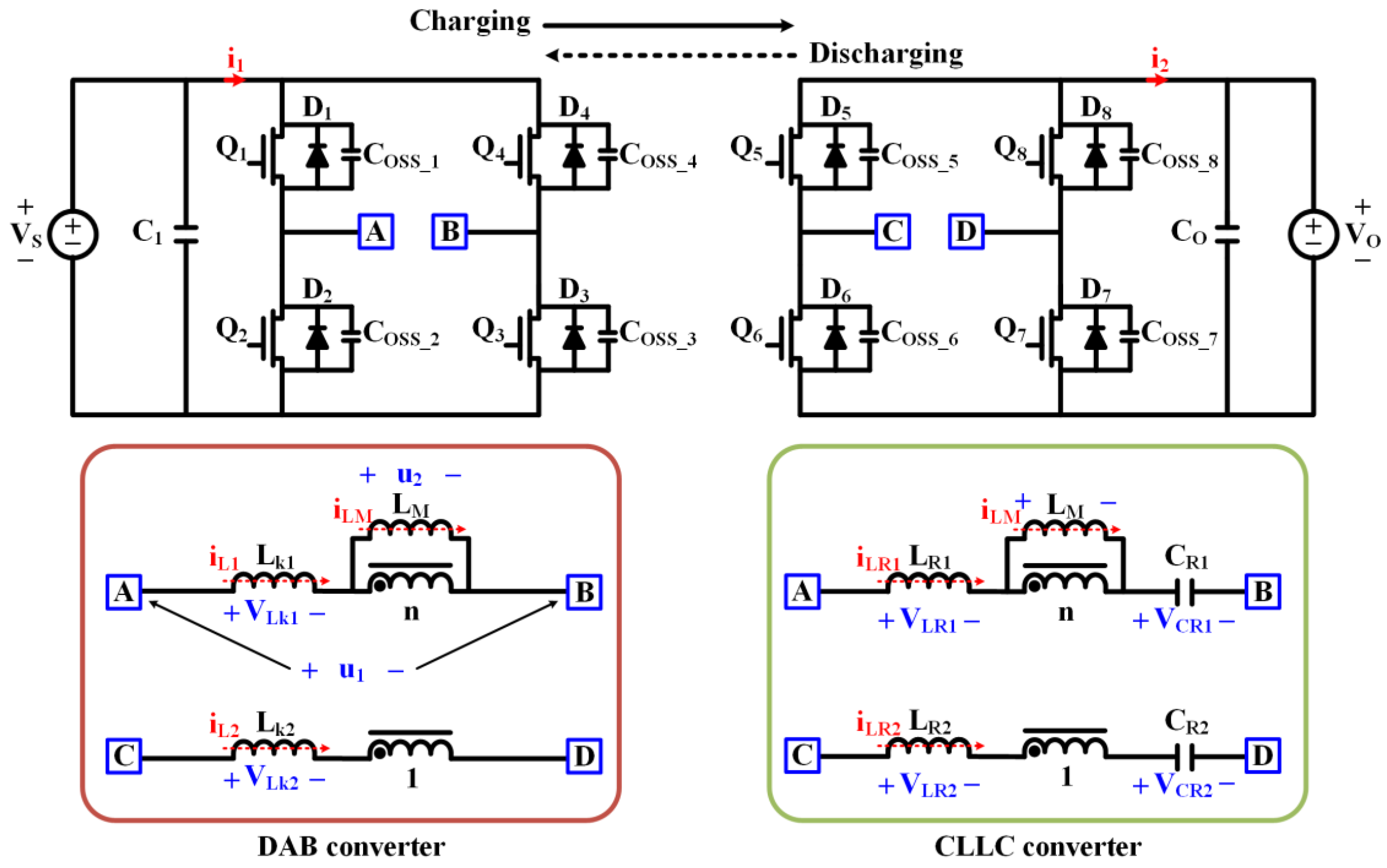
This article focuses on the charging of the dual active bridge (DAB) and CLLC converters. Figure 1 shows each topology which has a similar structure. But the CLLC includes a resonant capacitor CR in tanks on each side The tanks on each side are expressed as A to D in Figure 1. This section discusses the operating principle of each topology and a comparative analysis.
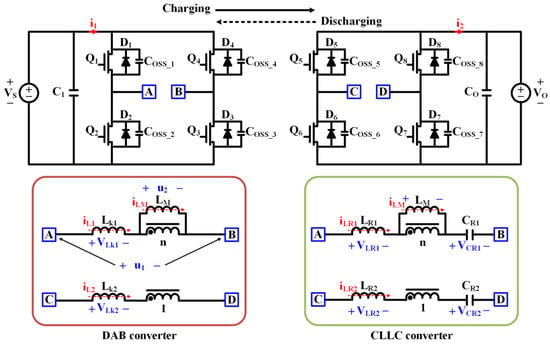
Figure 1.
The circuit diagram of each topology.
2.1. DAB Converter
The DAB has the advantage of bi-directional power conversion with a few components. As shown in Figure 2, the power is transferred through the equivalent leakage inductance , which is . Leq can be designed with lower inductance than hard-switching topologies such as buck converters and boost converters. Therefore, the DAB can achieve high power density while ensuring isolation.
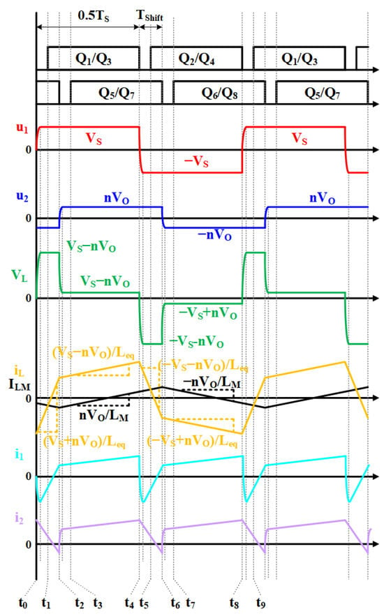
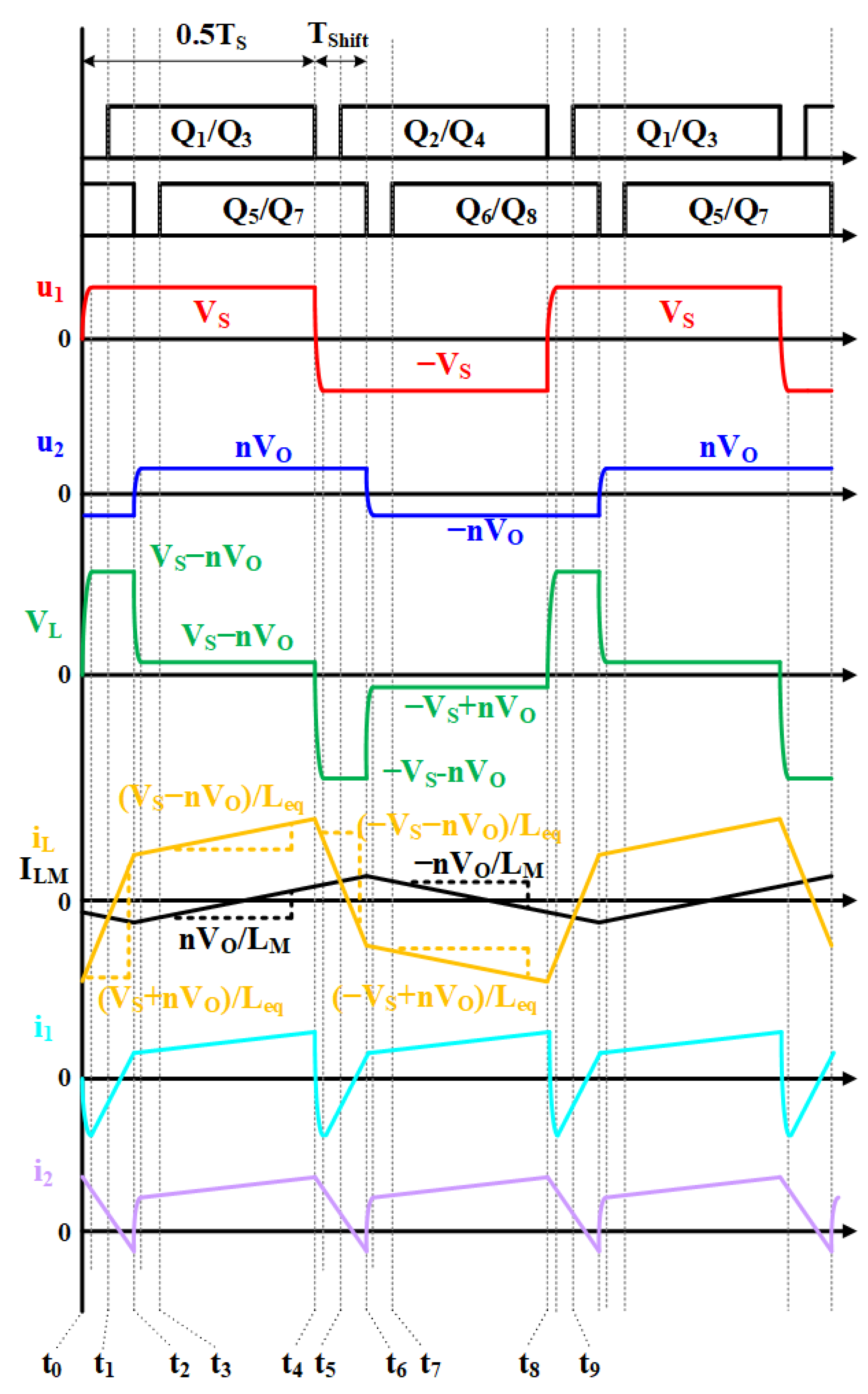
Figure 2.
The key waveforms of DAB.
For ease of mode analysis in the DAB, the following assumptions are made:
- The input and output voltage , is constant.
- The output capacitance is very large.
- The magnetizing inductance is significantly larger than the .
- The duty cycle of the DAB is denoted as and is defined as .
- The range of is 0 to 0.5.
Mode 1 [t0–t2]: In Mode 1, Q1, Q3, Q6 and Q8 are in the turn-on state during the interval t1 − t2. The voltage is applied to , and the secondary projected voltage is , applied to ; and increase/decrease linearly, where is a turn ratio. In this case, the slope of is . During the interval t0–t1, primary side ZVS can be achieved if the current is negative.
Mode 2 [t2–t4]: In Mode 2, Q1, Q3, Q5 and Q7 are in the turn-on state. The voltage is applied to , and the secondary reflected voltage is equal to and is applied to ; both and increase linearly. In this case, the slope of is . During the interval t2–t3, secondary ZVS can be achieved when the value of is positive.
Mode 3 [t4–t6] is omitted because it is symmetric to that in Mode 1.
The output power and gain of the DAB can be derived as follows:
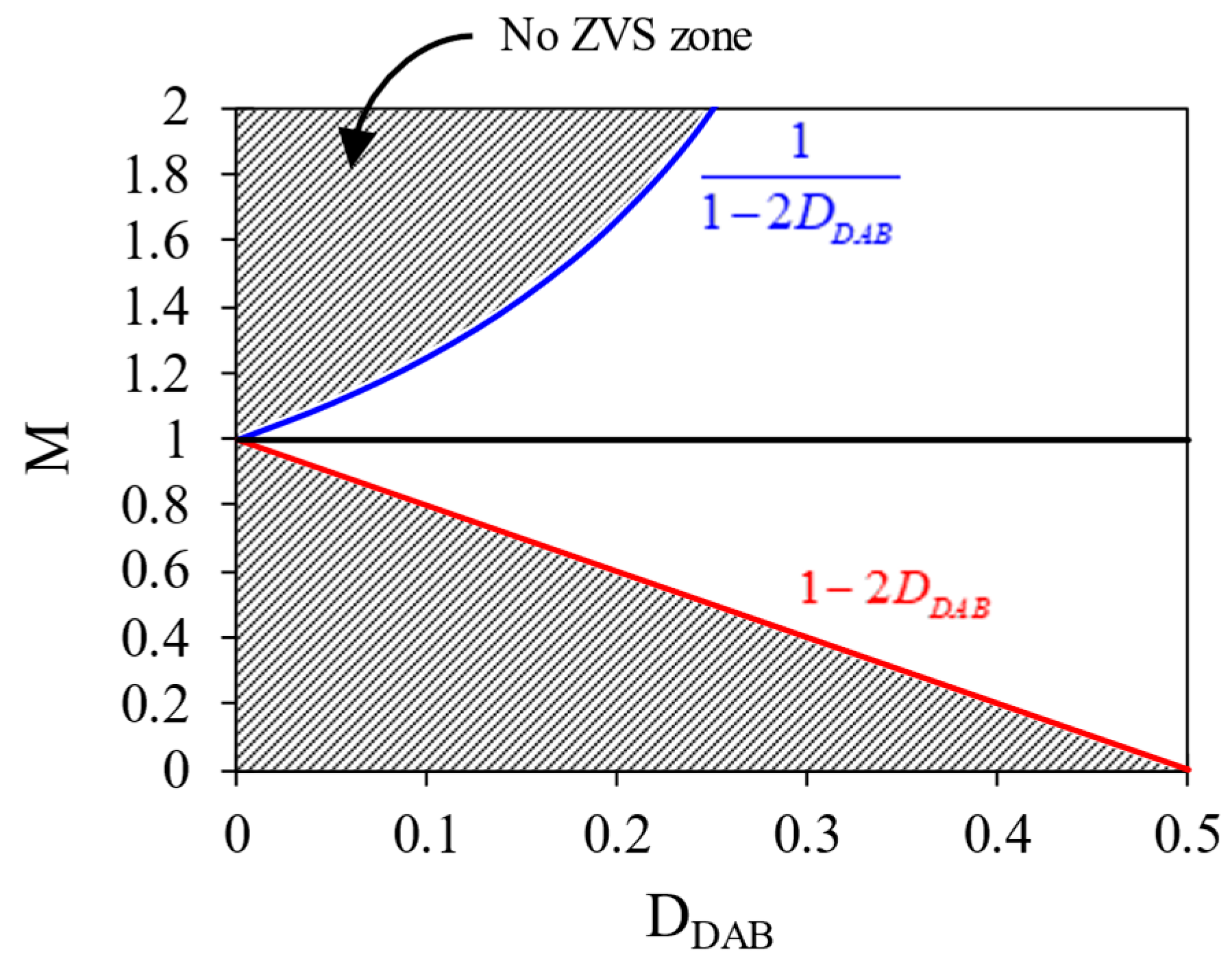
is the switching frequency. The soft-switching conditions in a DAB are shown in Figure 3. ZVS is achieved on both the primary and secondary sides when the is negative and is positive. Therefore, design points should not be included in the highlighted part of the curve below. If the design satisfies these conditions but lacks sufficient ZVS energy, switch turn-on loss may occur. It is important to satisfy the energy equation for ZVS during the period in which the switch is turned off. The equation is derived as follows:
where is the output capacitance in FETs. In Equation (3), is calculated as the input and output voltages, respectively.
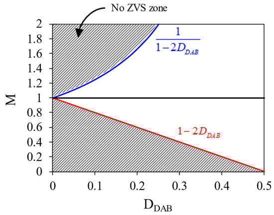
Figure 3.
ZVS region as and .
2.2. CLLC Converter
As shown in Figure 1, the CLLC consists of two resonant inductors and two resonant capacitors positioned on both the primary and secondary sides. The capacitors store energy and transfer it during the switching intervals, and the inductors form resonant circuits to achieve ZVS. Similarly to the DAB, the CLLC’s inductance can be substituted by the transformer’s leakage inductance. CLLC has a wide range of control of the battery voltage and facilitates soft switching of all switches over the entire load range.
For ease of mode analysis in the CLLC, the following assumptions are made:
- The input and output voltage , is constant.
- The output capacitance is very large.
- Instead of secondary side FETs switching, operation relies on the body diode, which is considered ideal.
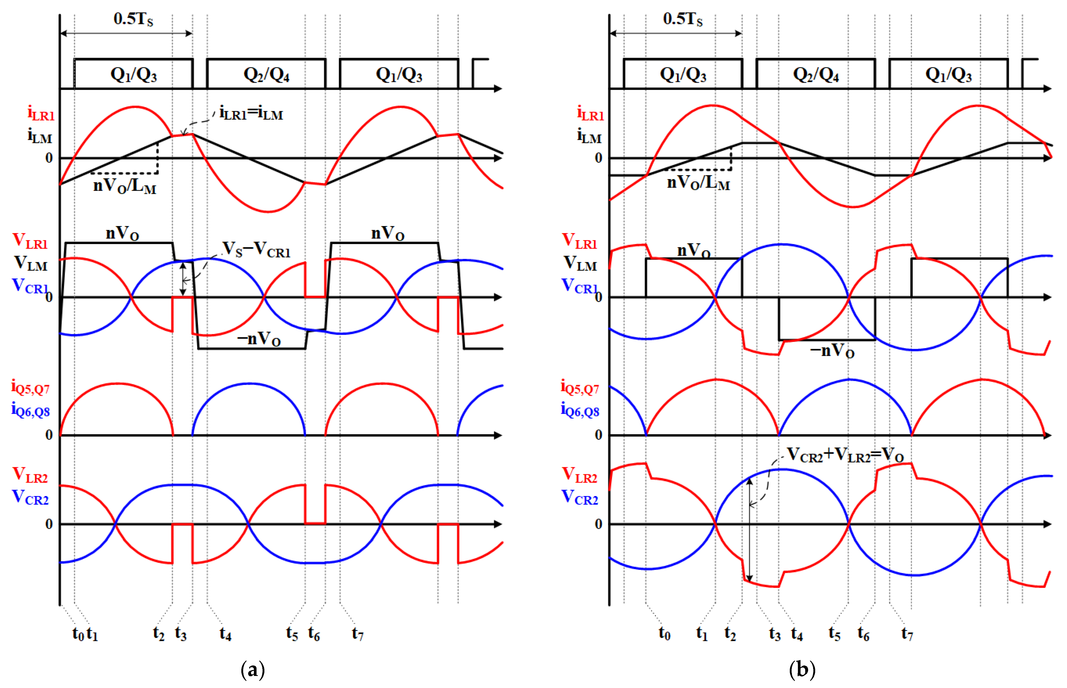
The key waveforms in the boost operation of CLLC are shown in Figure 4a. In this operation, the switching frequency is lower than the resonant frequency (: below region).
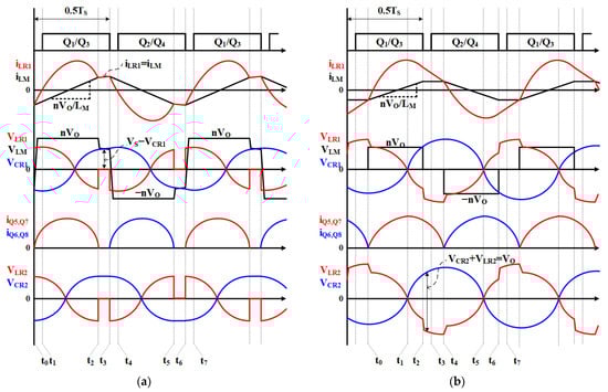
Figure 4.
The key waveforms of CLLC: (a) boost operation; (b) buck operation.
Mode 1 [t0–t2]: In Mode 1, Q1 and Q3 are in the turn-on state and Q2 and Q4 are in the turn-off state during the interval t1–t2. The current is , is applied to , and increases linearly. During this mode, resonance occurs between the primary resonant inductance and the primary side resonant capacitor , and does not participate in the resonance. for this mode is given by Equation (4). Meanwhile, during the interval t0–t1, ZVS is achieved on the primary side.
Mode 2 [t2–t3]: In Mode 2, Q1 and Q3 are in the turn-on state and Q2 and Q4 are in the turn-off state. The current is equivalent to , and is given by . During this mode, resonance occurs due to , and . The resonant frequency in Mode 2 of the boost operation is derived by Equation (5). Within this interval, the slope of and is zero due to , which corresponds to .
Mode 3 [t3–t5] is omitted because it is symmetric to that in Mode 1.
The key waveforms in the buck operation of CLLC are shown in Figure 4b. In this operation, the switching frequency is higher than (: above region).
Mode 1 [t0–t2]: this mode is identical to Mode 1 of the boost operation.
Mode 2 [t2–t3]: In Mode 2, Q1, Q2, Q3 and Q4 are in the turn-off state. is switching from to , resulting in being zero. Therefore, , which is , equals VO. During this mode, resonance occurs between and , and does not participate in the resonance. The resonant frequency in Mode 2 of buck operation is derived by Equation (6).
Mode 3 [t3–t4]: in Mode 3, Q2 and Q4 are in the turn-on state. Q1 and Q3 are in the turn-off state. As shown in Figure 4b, because is greater than , flows through Q5 and Q7.
Mode 4 [t4–t6] is omitted because it is symmetric to that in Mode 1.
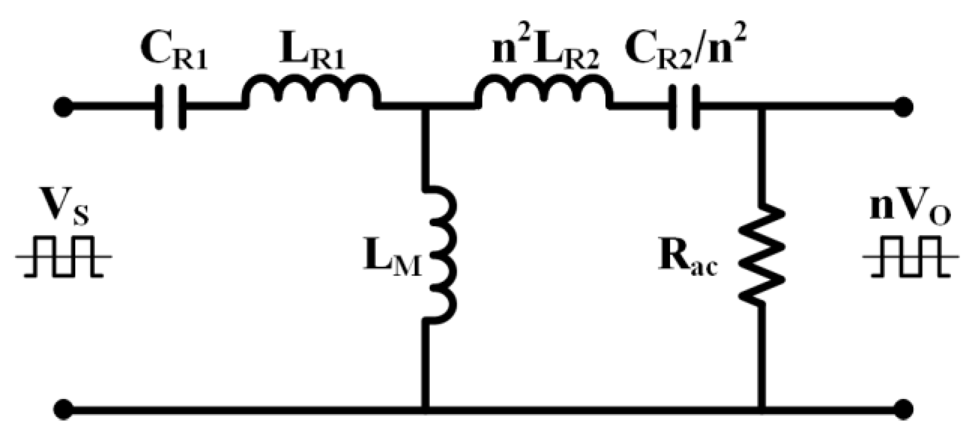
The gain of the CLLC can be derived through an equivalent circuit which is shown in Figure 5 [30]. can be derived as follows:
where
where is the quality factor and is the inductance ratio. The ac-equivalent load resistance using the first harmonic approximation (FHA) [30,31] can be calculated as
where is the RMS value of , which is the output voltage of the resonant network. is the RMS value of , which is the output current of the resonant network.
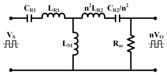
Figure 5.
Equivalent circuit of CLLC in charging mode.
As in DAB, the CLLC in buck operation must achieve ZVS during the turn-off state, as specified in Equation (3). In Equation (3), is calculated as . Meanwhile, in the boost operation, soft switching is ensured [30] because the switching frequency is lower than the resonant frequency , and the dead time can be derived as
2.3. Comparison in Operation Principle
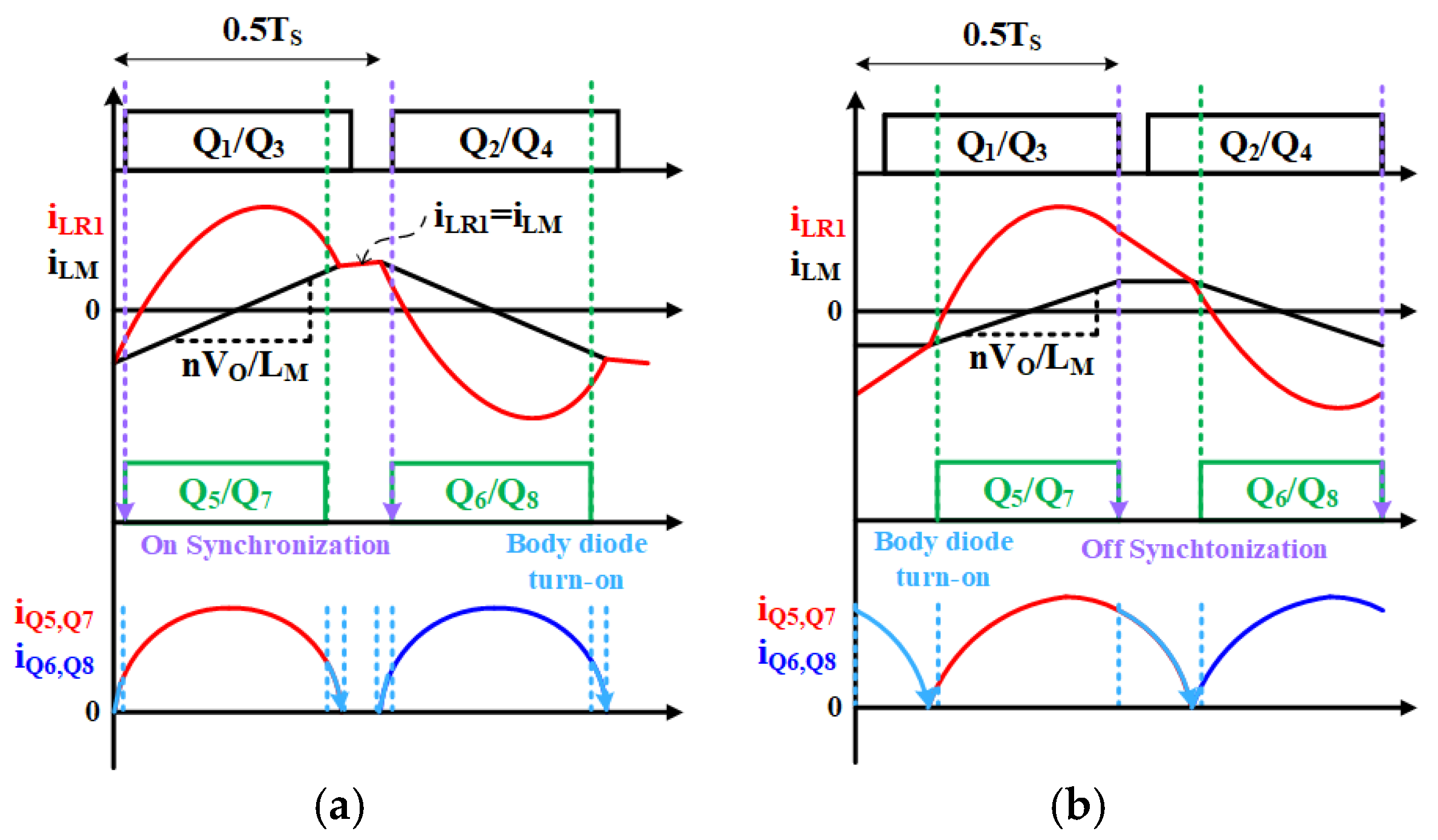
The comparison between the DAB and CLLCs is specified in Table 1. A DAB has a few components and is low in design complexity. Since the DAB gain has the same ratio as the load as in Equation (2), it is easy to regulate the gain. However, the slight phase shift makes soft switching difficult under light load conditions. Therefore, modulation strategies such as dual phase shift (DPS) and triple phase shift (TPS) have been proposed for soft switching under full load conditions [32,33,34,35]. This article has adopted the traditional modulation method, a single phase shift (SPS), to focus on the conventional DAB topology. In contrast, the CLLC requires more components than the DAB. The design complexity of the CLLC is higher than that of the DAB because the gain of the CLLC depends on the Q and K factors [30]. Modulation of CLLC is frequency control and soft switching is achievable under full load conditions [13,36,37]. Furthermore, the CLLC maintains an ideal secondary side switching boundary, resulting in higher efficiency than the DAB. Meanwhile, the typical modulation strategy of the CLLC is synchronization rectification (SR) driving [36,37,38,39,40]. Reference [37] proposes a dual-active-synchronization (DAS) modulation strategy to address current distortion. However, as mentioned above, this article focuses on the comparison between conventional DAB and CLLC; thus, typical SR driving is applied. The SR driving in this article is shown in Figure 6. In the below region, the secondary side switch synchronizes with the turn-on of the primary side switch and turns off earlier than the primary side. In the above region, the secondary side switch synchronizes with the turn-off of the primary side switch. To minimize the conduction loss of the body diode of the secondary side switch, it should be timed to coincide with the zero-crossing moment of the secondary current. However, as this is another research topic [39,40], this article adopts a simplified SR driving that allows for the interval of the secondary side body diode turn-on. As mentioned, this article adopts the simple and typical bi-directional topologies and control method. A more advanced control method could reduce the secondary side switch losses in the CLLC.

Table 1.
Comparison of DAB and CLLC.
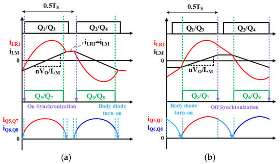
Figure 6.
Modulation method in CLLC convert: (a) in below region; (b) in above region.
3. Design Considerations
3.1. Design Direction—Design Parameters
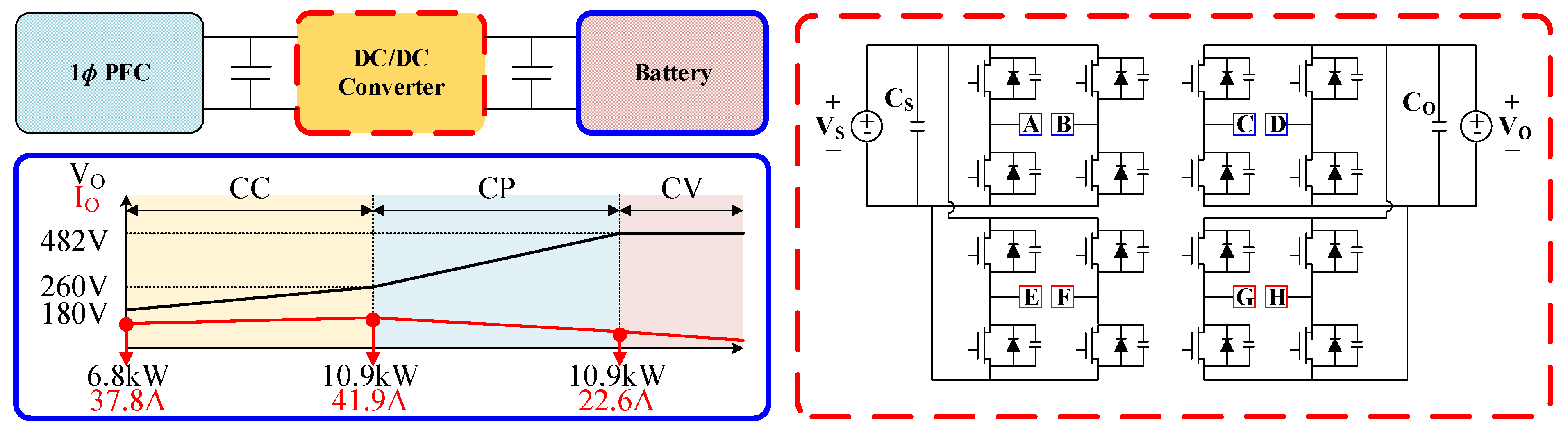
A simple configuration of the system and the battery specifications are illustrated in Figure 7. It consists of a one-phase PFC, a DC-DC converter, and a battery. Since the main purpose of this article is to the DC-DC stage, the design process started with the output of the PFC stage. The specification of battery is shown in the blue box of Figure 7. Also, the overall specifications and target of the OBC system are detailed in Table 2. If the DC-DC stage operates with only one module in the 400 V-class battery system, it can generate a high RMS current which can damage the FETs. To avoid damaging the FETs, the DC-DC stage consists of two parallel modules, as shown in the red dash box of Figure 7. This configuration is essential because conduction loss is proportional to the square of the current. Also, the feature of this article is that both topologies use the transformer’s leakage inductance without additional inductors. On the other hand, the switching loss is limited to 24 W, which is a value that considers a margin of 1/20 of the power dissipation PD at 100 °C of GS66516B (Infineon, Munich, Germany).
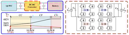
Figure 7.
Simple configuration of OBC DC-DC stage.
Table 2.
System specifications and targets of OBC.
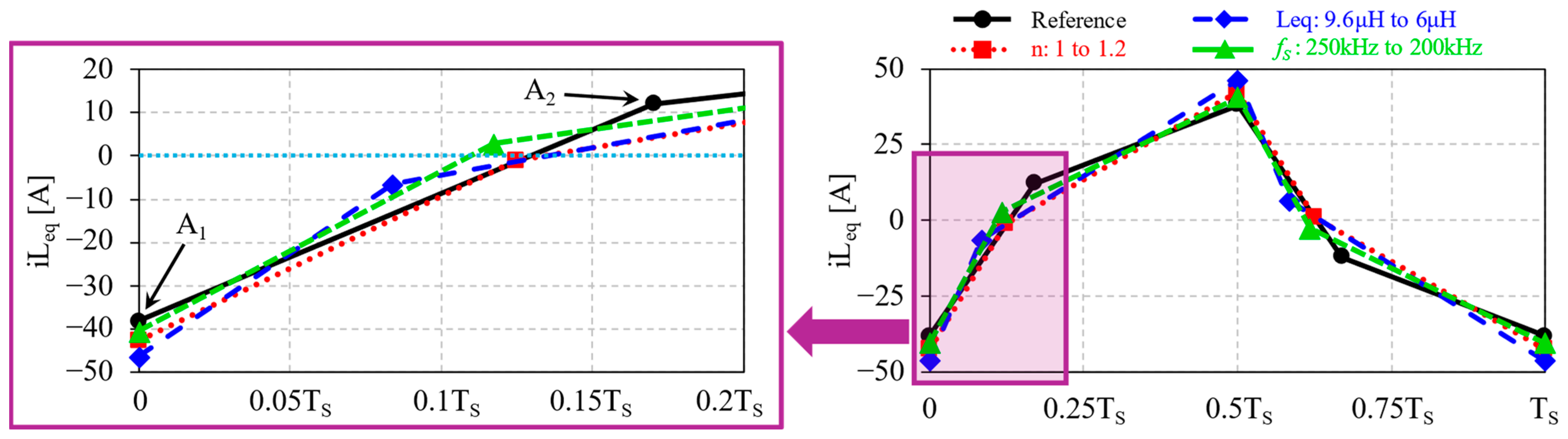
The DAB and CLLCs are designed based on Table 2. Before proceeding with the design of each topology, it is essential to understand the design direction of each converter. The design parameters of the DAB can be selected as , , , and the is based on Equation (1). Figure 8 shows the curve obtained by regulating the design parameters. To confirm the change in the curve, the condition should be selected where is the greatest. It is the endpoint of the constant current (CC) region which is = 450 V and = 260 V, as shown in Figure 7. The reference design parameters in Figure 8 are as follows: is 1, is 9.6 μH, and is 250 kHz. The characteristics are analyzed when increased or when or decreased relative to the reference, and the analysis for each case is presented in Table 3. The ZVS of the secondary side switches tends to be unachieved when the is increasing, is decreasing, or is decreasing. To identify the optimal design parameters, each of the three design parameters were individually increased or decreased to find the appropriate design point. When designing the range from 0.1 to 0.4 with a margin of less than 0.5, it is necessary to design a ZVS that satisfies all switches to minimize the loss. Therefore, the optimal design parameter of the DAB is selected as the reference value when considering the input/output range, range, and ZVS achievement.
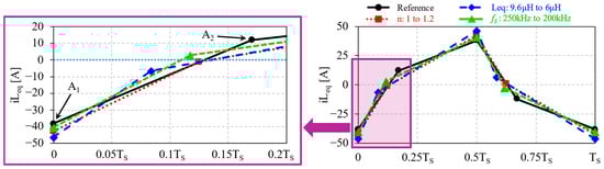
Figure 8.
Regulating design parameters in DAB.
Table 3.
Value of regulating design parameters in DAB.
The design parameters of the CLLC may be selected as , , the resonant frequency , the magnetizing inductance , the primary leakage inductance , the inductance ratio , the quality factor , and the ac-equivalent load resistance based on Equations (7)–(11). In this case, the design parameters in the resonant tank, such as and , can be derived as
Due to the large number of design parameters, it is important to identify the direction of the design. Therefore, the design direction was confirmed by regulating the design parameters of the CLLC as shown in Table 4 and Figure 9. The reference design parameter in Figure 9a is as follows: is 1.2, is 35 μH, is 7.7 μH, is 82 nF, and = 250 kHz. If is set to 1, the CLLC will operate in the buck operation, which causes increasing switching loss by using a high switching frequency. Therefore, in this paragraph is set to 1.2—a number greater than 1 for design direction. Figure 9a is a reference gain curve. Additionally, the different two gain slopes indicate the inductive and capacitive regions, with ZVS achievement in the inductive region [30]. Therefore, the design direction should aim at the inductive region. Figure 9b shows the case where and are constant, but and increase at once. In (b), the slope increases in the below region compared to (a) and decreases in the above region. This means becomes high. The increased leads to reduced , thus decreasing switch turn-off loss in the below region. Figure 9c shows the effects of increasing while keeping and constant. is reduced to maintain , resulting in increased , and the capacitive region becomes wider, complicating the selection of a design point. Figure 9d shows increasing while keeping and constant. In this case, the slope increases in both the below and above regions. Like (b), this leads to reduced turn-off loss. Figure 9e shows increasing only while keeping other design parameters. In (e), becomes low as increases. This means the required switching frequency range will be wide. In summary, the changing trend of the gain curve has been confirmed by regulating design parameters such as and . In each case, the loss varies depending on the required switching frequency range, so a design with proper design parameters is needed.
Table 4.
Value of regulating design parameters in CLLC.
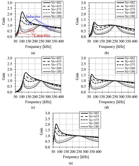
Figure 9.
Regulating design parameters in CLLC: (a) reference gain curve; (b) constant and , increased and ; (c) constant and , increased ; (d) constant and , increased ; (e) increased and constant others.
3.2. Design Direction About Transformer
The design direction for the DC transformer (DCX) of each topology was analyzed. The DAB when the turn ratio is 1, and the should be selected to satisfy the required range and ensure ZVS for all switches. Increasing and can reduce switching loss. However, these factors are not only related to switching loss but also to the DCX size. To reduce the DCX size, a smaller and higher should be chosen. However, an excessively small can lead to unachieved ZVS, resulting in increased switching loss. Conversely, too high increases turn-off loss. This also increases the RMS current, leading to higher conduction loss in the switches, and demands a larger wire diameter in the DCX. Additionally, an overly high can increase core loss. Therefore, the final DAB design parameters are presented in Table 5. These parameters are the result of analysis according to the design direction to satisfy the required power density and efficiency.
Table 5.
Final design parameters of DAB.
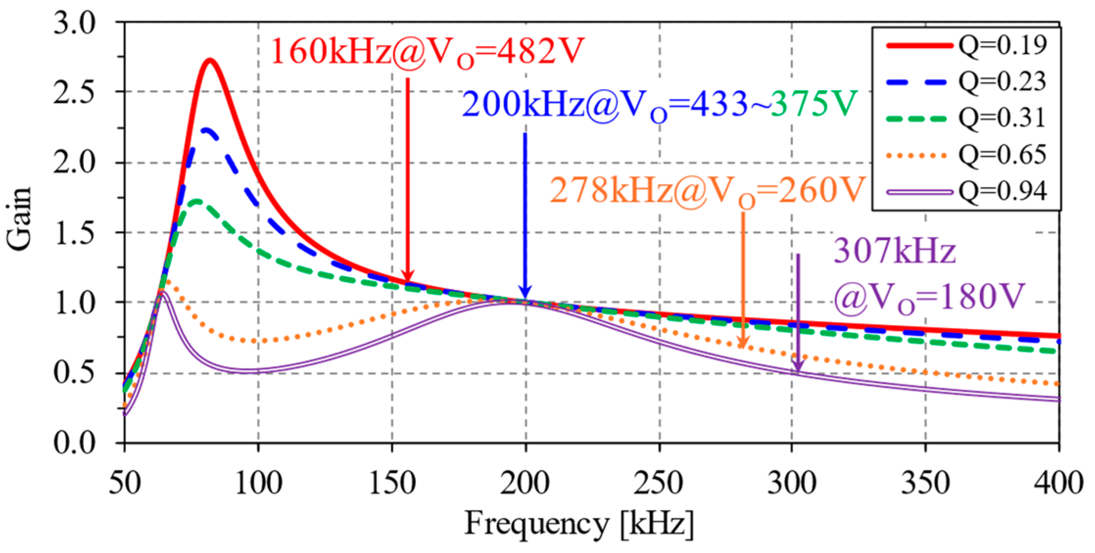
Similarly, the DCX of the CLLC should be designed with the same method as the DAB. As shown in Figure 9b,d, adopting the below region can reduce switching loss, but it requires a larger DCX cross sectional area. Given the limited power density, it is not feasible to increase the core size. Therefore, it is important to select the range of the above region while satisfying the limited switching loss, which is the abovementioned 24 W. Consequently, the final CLLC design parameters and gain curve are shown in Table 6 and Figure 10. The input/output voltage range by the final design of each topology is shown in Figure 11.
Table 6.
Final design parameters of CLLC.
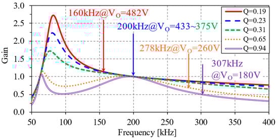
Figure 10.
Gain curve of CLLC.
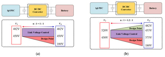
Figure 11.
Configuration of system and input/output voltage range in dotted boxes regarding each topology: (a) DAB; (b) CLLC.
Based on the previous design specifications, the DAB has adopted a separated winding structure for the DCX to utilize the leakage inductance, as shown in Figure 12a. The specifications and simulation results of the DAB-DCX are presented in Table 7. The performance of the DAB-DCX is evaluated using an FEA-based simulation tool at points where core and winding losses are at their maximum. As shown in Figure 12b,c, the maximum magnetic flux density in the cross section of the central leg is 0.089 T under the maximum flux density condition, which occurs at the maximum output voltage ( = 482 V), and 0.057 T under the maximum current density condition, occurring when the output voltage is 260 V. The results derived from theoretical calculations and those obtained through simulation are each documented in Table 8. Additionally, simulations could provide insights into losses due to the eddy effect, which are difficult to check through calculations alone.
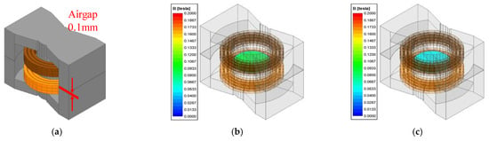
Figure 12.
Modeling and distributions of flux density in DAB-DCX: (a) modeling; (b) flux density at = 482 V; (c) flux density at = 260 V.
Table 7.
Design specifications of DAB-DCX.
Table 8.
Results of theoretical calculations and simulations in DAB-DCX.
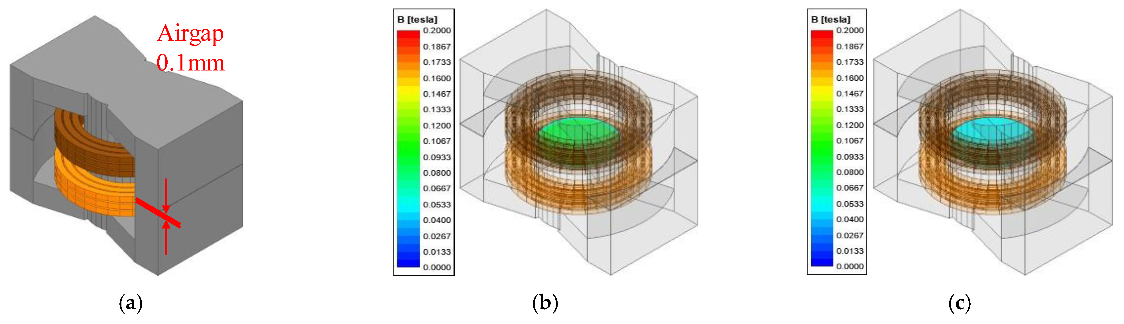
To match the power density, the CLLC-DCX was designed using the same core as the DAB-DCX. As shown in Figure 13a, the winding structure is similar to DAB-DCX to utilize the DCX’s leakage inductance. The airgap was regulated to control the magnetizing inductance. The specifications and simulation results of the CLLC-DCX are presented in Table 9. The DCX loss is confirmed under both maximum flux density and maximum current density conditions, with the flux density distribution shown in Figure 13b,c. Table 10 summarizes the flux density for each condition and compares the results from theoretical calculations and simulations in CLLC.
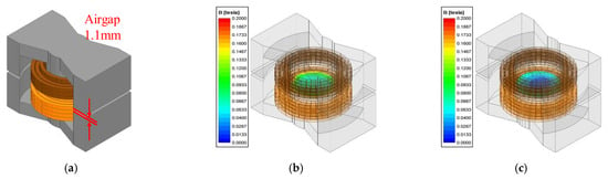
Figure 13.
Modeling and distributions of flux density in CLLC-DCX: (a) modeling; (b) flux density at = 482 V; (c) flux density at = 260 V.
Table 9.
Design specifications of CLLC-DCX.
Table 10.
Results of theoretical calculations and simulations in CLLC-DCX.
In conclusion, DAB and CLLC are designed under the same constraints, which are input/output voltage range and power density. DAB’s design parameters are relatively few with , , and . A wide input/output range and ZVS can be satisfied through is 1.
However, in CLLC, the design parameters are , , , , , and the gain is very complicated. is above 1 for the narrow frequency range because modulation control of CLLC is a switching frequency. Additionally, a minimum = 450 V covers a wide range which is from 180 V to 482 V. Moreover, by regulating the design parameters, all conditions must satisfy the inductive region to achieve ZVS for all switches. Additionally, the must be selected to ensure that the voltage stress on is not high and that the size of the DCX is not excessively large. In addition, since it is disadvantageous in the switching loss caused by SR driving, an airgap was added to satisfy the , in the CLLC-DCX design, and the eddy loss of the winding due to the fringing effect is greater. In conclusion, from the analysis of the design, it is expected that DAB will be more efficient in the experiment than CLLC.
4. Experimental Results
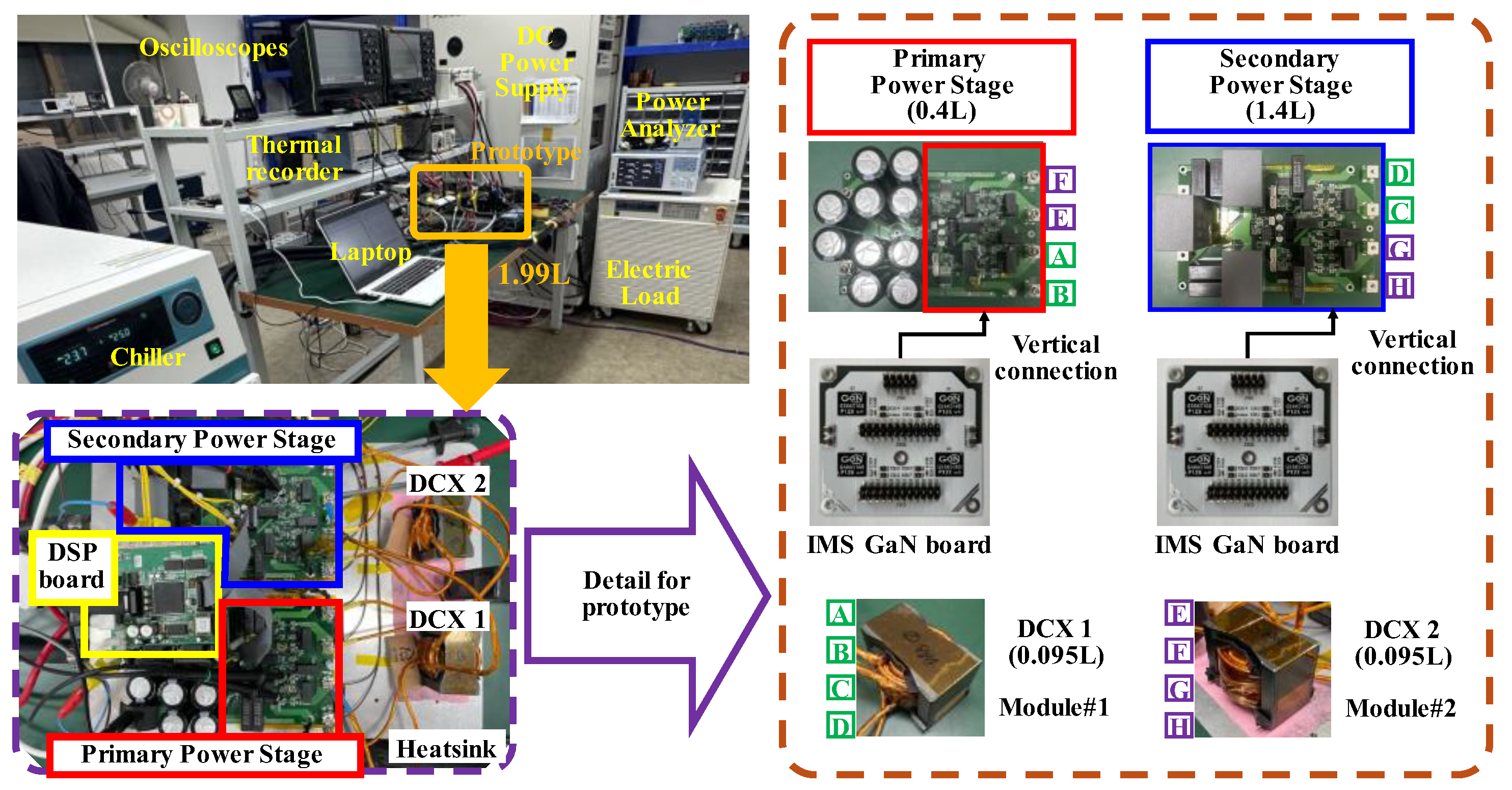
A prototype with a power density of 5.5 kW/L is manufactured. A photo of the DC-DC stage and testbed is shown in Figure 14. The input power supply used to drive the DC-DC stage is the AINUO ANEVH 4500-40(F) (Republic of Korea), and the electronic load is the PRODIGIT 34315E (Taiwan). Efficiency measurements are taken using the YOKOGAWA WT5000 (Japan). The YOKOGAWA GP10 (Japan) shows the temperature of switches. The GaNFETs were used which use GaN SYSTEMS GS66516B cooled using an insulated metal substrate (IMS) board, and each module of the power board was vertically mounted. A JOTEC HH-35 (Republic of Korea) chiller is used for cooling the GaN board. The inductance of the DCX was measured using HIOKI IM3533 (Japan). The measured inductance of the DCX and resonant capacitors is shown in Table 11. In the DAB-DCX, the magnetizing inductance is 213.5 µH, and the equivalent inductance is 9.2 µH. In the CLLC-DCX, the magnetizing inductance is 39.03 µH, and and are 5.85 µH and 6.86 µH, respectively. Therefore, the resonance frequency of the CLLC was regulated to 200 kHz by tuning the resonant capacitors, the was 108 nF and the was 92 nF. At this point, due to changes in and , the switching range in the experiment differed from the designed switching range.
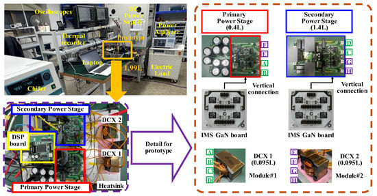
Figure 14.
A photo of testbed.
Table 11.
Prototype of specifications for each converter.
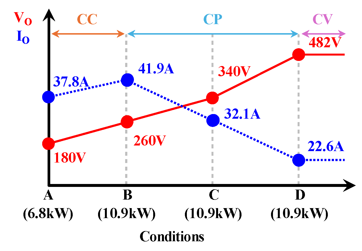
To compare DAB and CLLC, experimental conditions with 400 V-battery specification are selected, as shown in Figure 15. The two reasons for selecting these conditions are as below. First, we compare each topology under the conditions of the minimum battery voltage (condition A), maximum current density (condition B), and flux density (condition D). Condition C is a nominal condition because it needs to be checked because it is in the middle of the CP. Second, this article proposes the OCB DC-DC stage for the 400 V-battery system. The abovementioned battery specification is produced by Hyundai, Tesla, Volkswagen, etc.
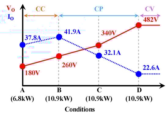
Figure 15.
Experimental cases under 100% load condition.
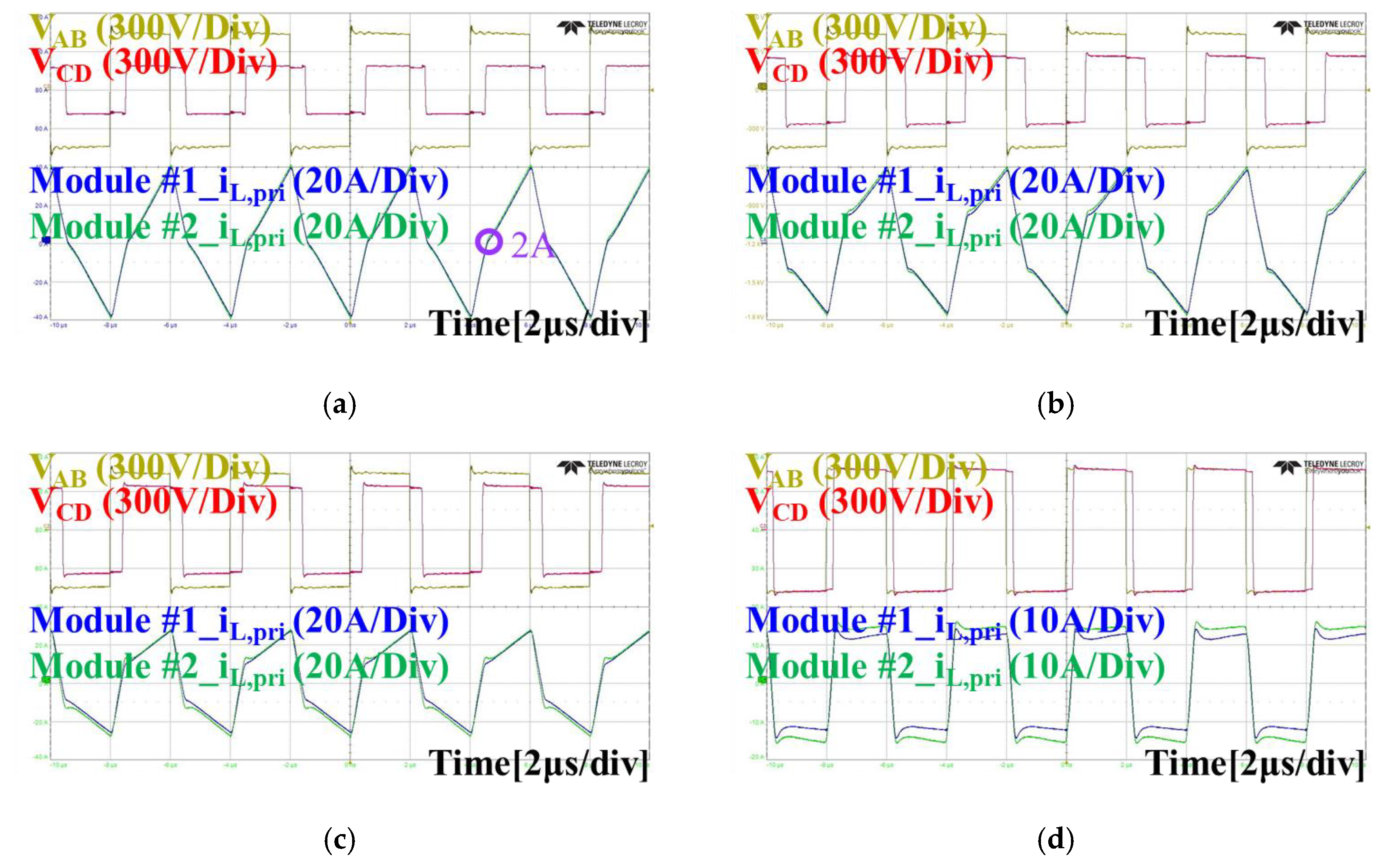
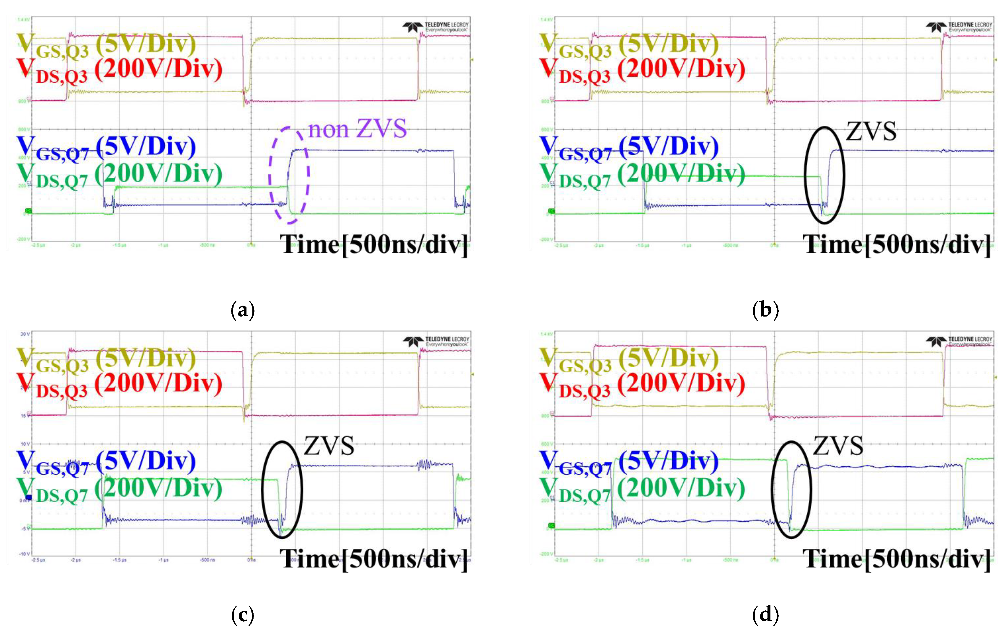
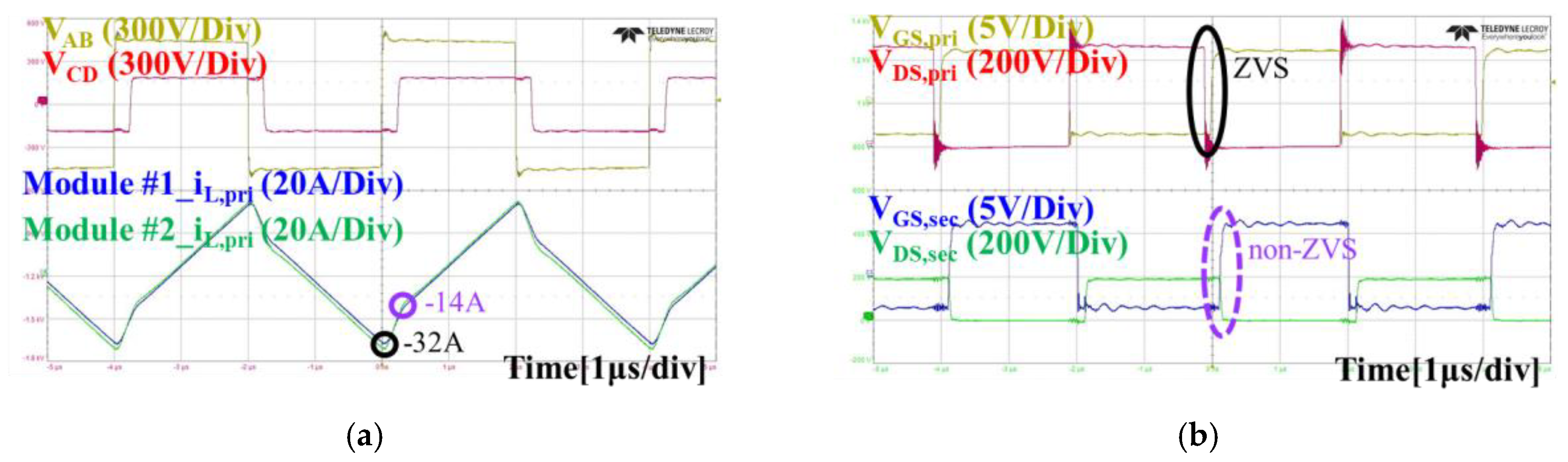
Figure 16 illustrates the key waveforms under each condition for each topology under 100% load. In condition A, ZVS on the secondary side of the DAB is not achieved, as shown in Figure 16. The highlighted section in Figure 16a shows the gate-source and drain-source voltages of the secondary side. This occurred because the inductance of the DAB-DCX prototype is smaller than the designed value 9.6 μH, reducing the . As verified in Section 2, even though has a positive value, it does not satisfy Equation (3). On the other hand, the ZVS achievement under other conditions can be confirmed in Figure 17.
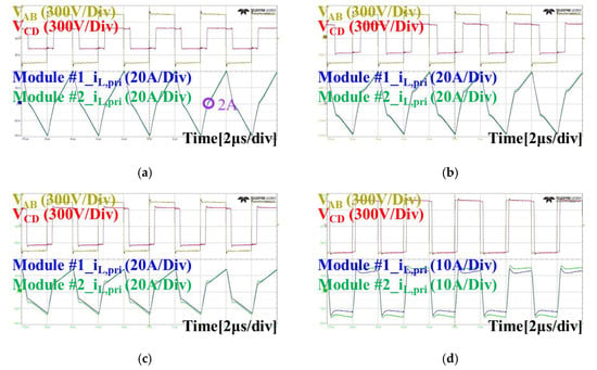
Figure 16.
Operational key waveforms in DAB: (a) condition A at 39.24°; (b) condition B at 58.32°; (c) condition C at 36.72°; (d) condition D at 21.24°.
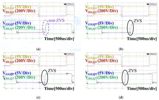
Figure 17.
Operational key waveforms regarding ZVS achievement in DAB: (a) condition A; (b) condition B; (c) condition C; (d) condition D.
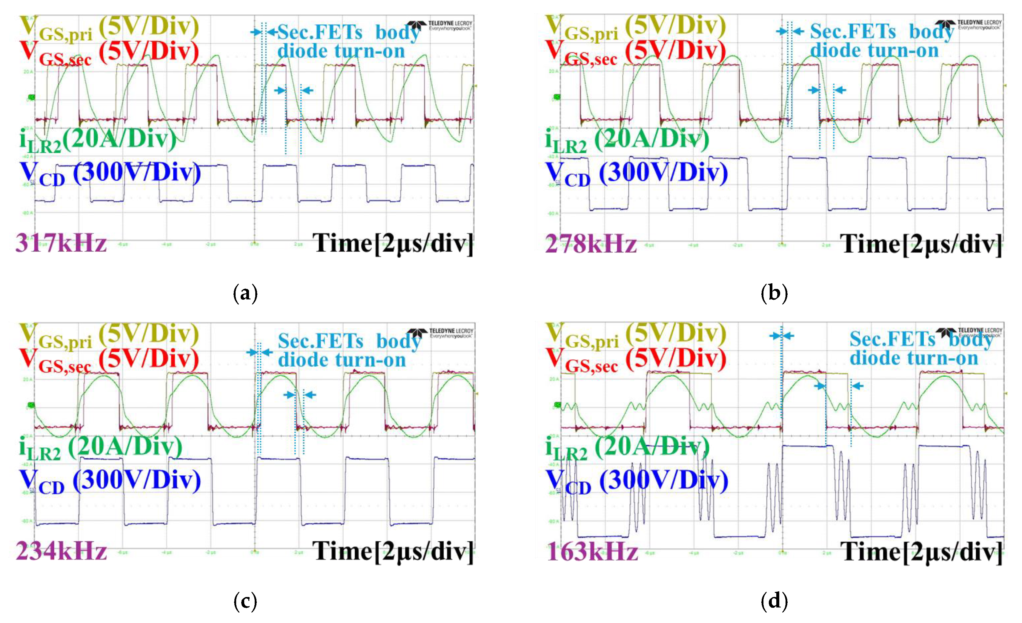
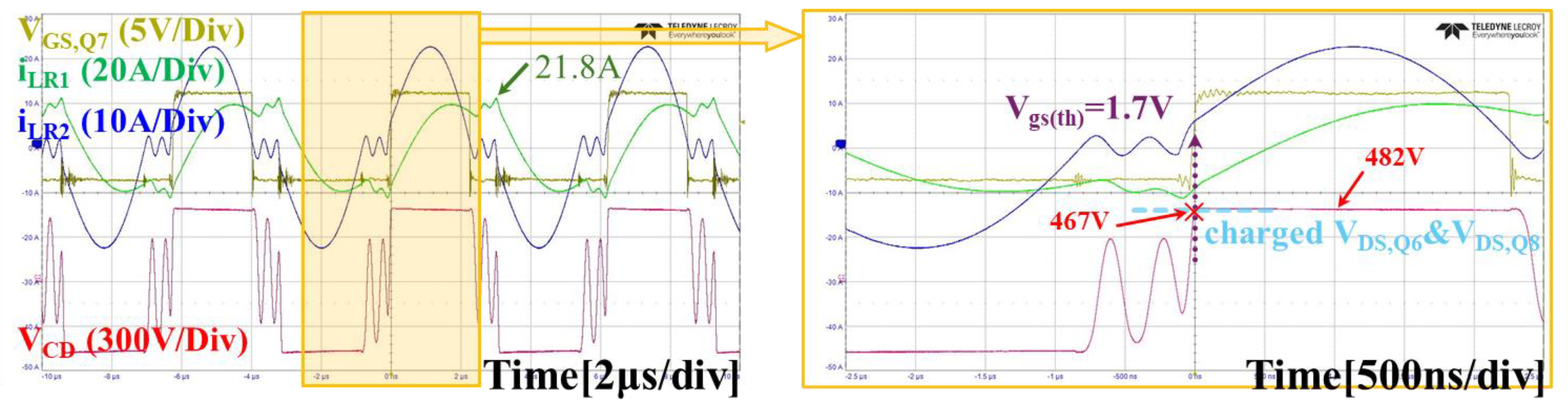
Figure 18 shows the key waveforms under each condition for CLLC under the 100% load condition. Figure 18a–c operate in the above region, where the turn-off current is large, enabling ZVS. On the secondary side, soft switching is possible because the body diode of the secondary side switch states turn-on. On the other hand, (d) operates in the below region. This waveform can be analyzed in relation to Section 2. In the below region, and converge, making the turn-off current equal to . Based on the measured magnetizing inductance and switching frequency, the maximum value of is calculated to be about 22 A. The measurement points are changed to review this, as shown in Figure 19. Since sufficient energy is available to achieve ZVS, the ZVS of the primary side switch can be confirmed, as shown in Figure 19. The secondary side switch is synchronized with the turn-on of the primary side switch. The gate-to-source threshold of the GS66516B is 1.7 V, indicated by the dashed arrow in Figure 19. At this point, had reached 97% of the output voltage (482 V), meaning that the drain-to-source voltage of Q6 and Q8 had charged, allowing Q7 to achieve almost ZVS. Meanwhile, oscillation occurs when the secondary side gate is turned off. This is caused by the resonant inductor and the parasitic capacitance of the secondary side switches [40].
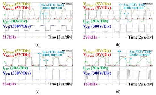
Figure 18.
Operational key waveforms in CLLC: (a) condition A at 317 kHz; (b) condition at 278 kHz (c) condition C at 234 kHz; (d) condition D of CLLC at 163 kHz.
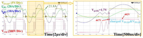
Figure 19.
Operational key waveform at condition D in CLLC.
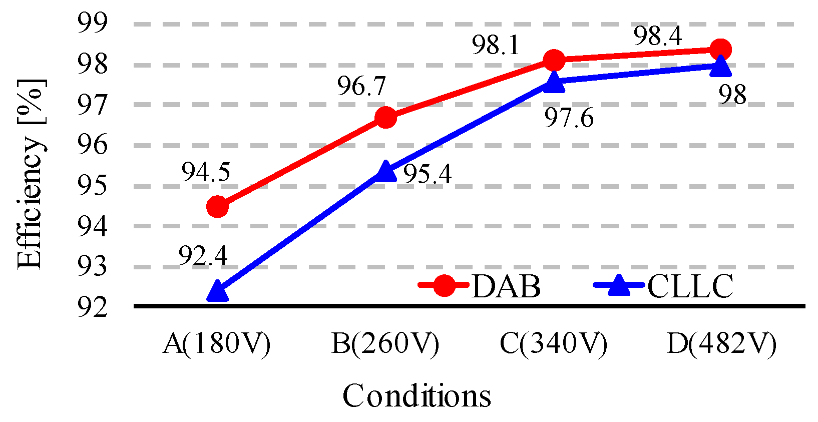
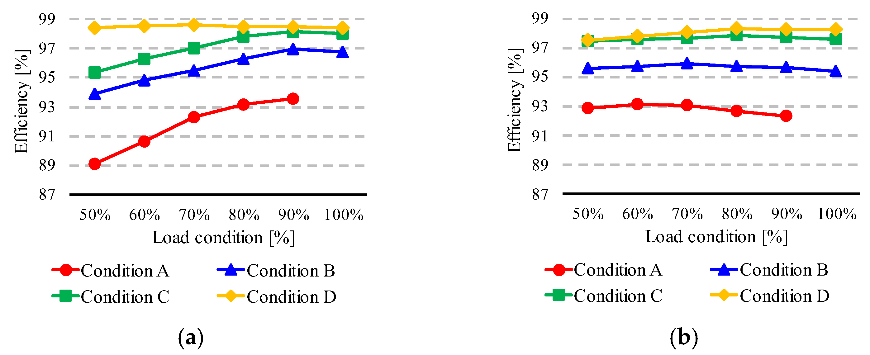
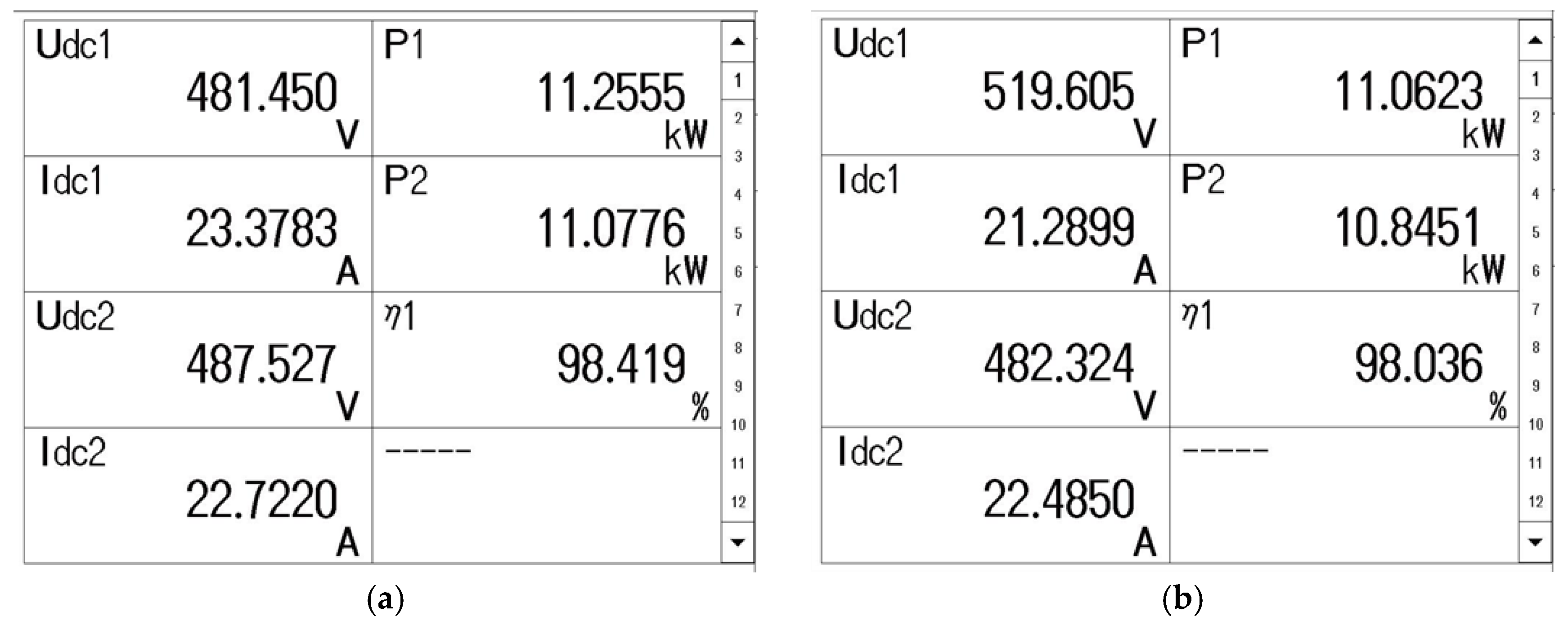
Figure 20 presents the efficiency graphs corresponding to each condition. Figure 21 shows the experimental efficiency under various load conditions. Additionally, Figure 22 shows the actual measurement efficiency of each topology at condition D. The load conditions are selected from 50% to 100% to observe the variation trend under light load. Overall, the DAB shows higher efficiency under 100% load. However, under light load, the CLLC has higher efficiency. The analysis of experimental results is presented in Section 5.

Figure 20.
Efficiency by conditions and each topology under 100% load.

Figure 21.
Efficiency of each topology by conditions and load conditions: (a) DAB; (b) CLLC.
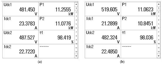
Figure 22.
Efficiency at condition D using WT5000 under 100% load: (a) DAB; (b) CLLC.
5. Analysis of Experimental Results
5.1. Switch Loss
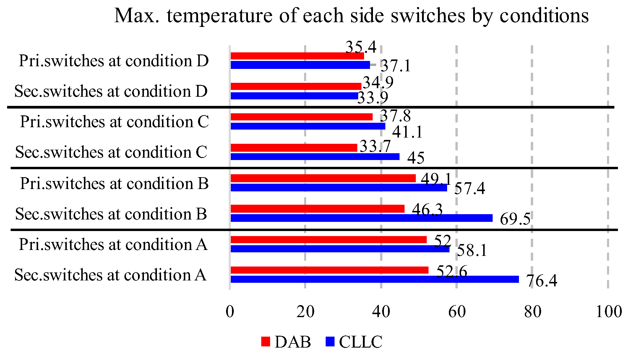
The blue dashed line in Figure 18 is the turn-on state of the secondary switches’ body diode. It should be the conduction loss of the body diode. Therefore, the secondary side switches will have a higher switching loss. This loss is related to the heat. Figure 23 shows the maximum temperature of each side switch by each topology.
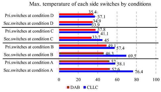
Figure 23.
Maximum temperature of switches under 100%.
The CLLC, which is a resonant topology, has high current RMS value, so it has a higher temperature than the DAB. Meanwhile, ZVS was not achieved for the secondary side switches in condition A in the DAB because the equivalent inductance of the DAB-DCX prototype is smaller than the designed inductance. Nevertheless, the switch temperature of the DAB is lower. The switch temperature of CLLC is higher because the conduction loss by the high-current RMS and body diode is larger than the turn-on loss. However, under light load conditions, the CLLC has a higher efficiency. As shown in Figure 24, the DAB does not achieve ZVS under light load conditions, resulting in increased turn-on loss for the secondary side switches. Meanwhile, the CLLC satisfies ZVS under light load conditions, resulting in lower losses.
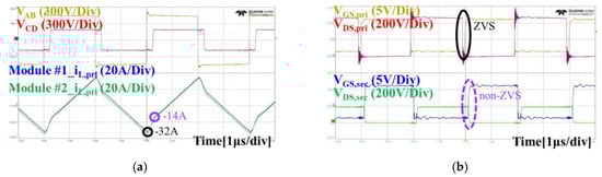
Figure 24.
Operational key waveforms under 50% load in DAB: (a) voltage and current waveform of DAB-DCX; (b) gate-source and drain-source voltage of each side.
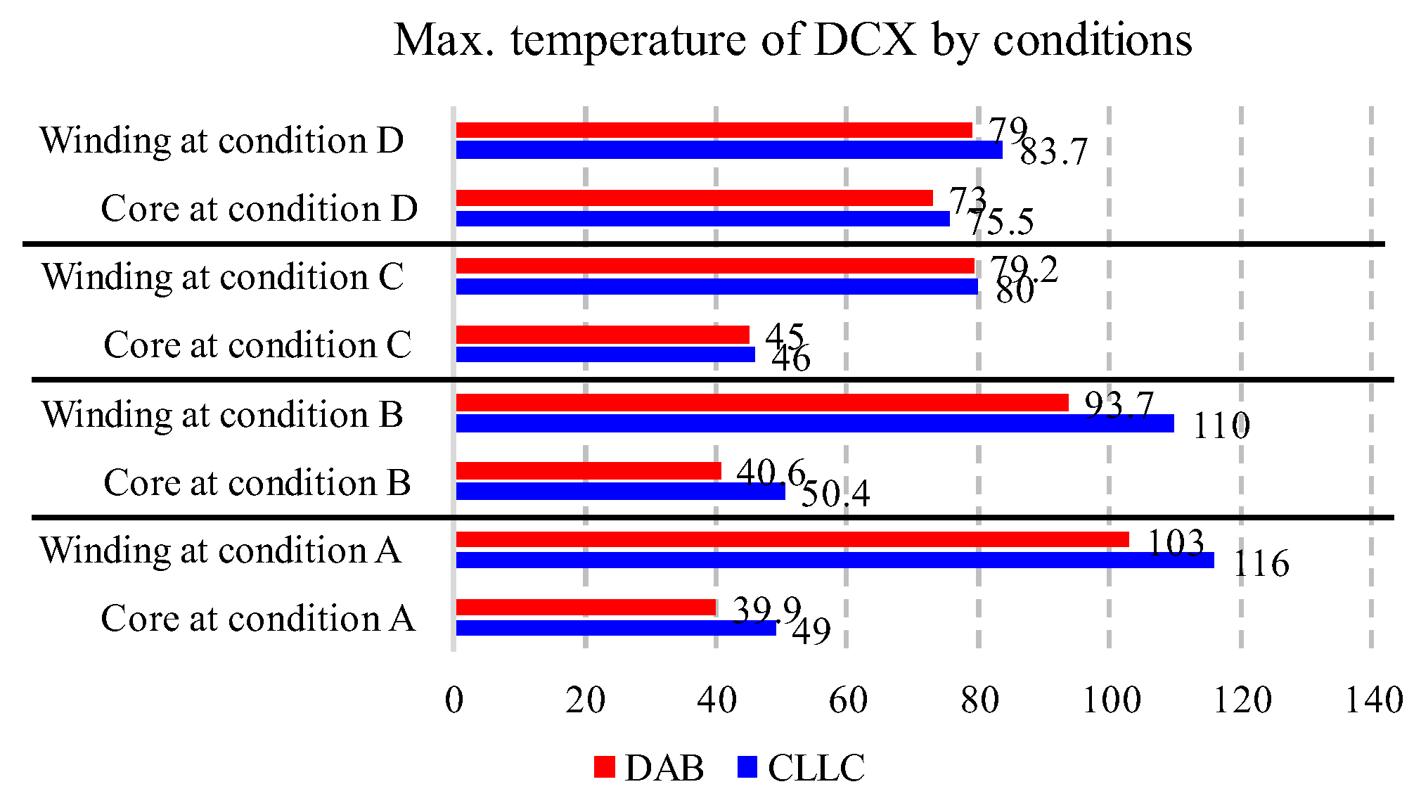
5.2. DCX Loss
CLLC-DCX causes a more significant winding loss due to the fringing effect caused by the airgap of 1.1 mm. This airgap is to satisfy the magnetizing and leakage inductance requirements. In contrast, the winding loss of the DAB-DCX is low because of the smaller airgap than the CLLC-DCX. In short, the larger airgap causes more winding eddy loss in CLLC-DCX. Therefore, the loss is related to the heat, and Figure 25 shows the maximum temperature of DCX. The temperature is measured by FLIR E54 (OR-U.S.), which is a thermal imaging camera. The measurement points of temperature are the top of the core and the surface of the winding. Under conditions of high current density, the winding temperature increases, and with higher flux density, it can be observed that the core temperature tends to rise as well.
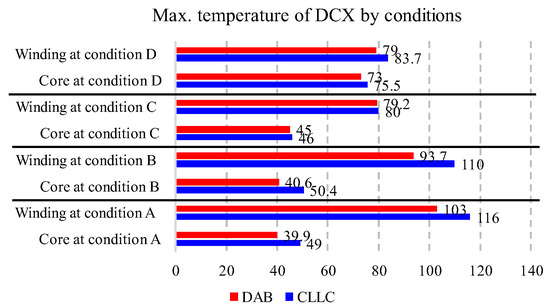
Figure 25.
Maximum temperature of DCX under 100%.
5.3. Differences in Control and Comprehensive Analysis
The DAB has phase shift modulation, but the CLLC has frequency modulation and secondary side SR driving. SR driving is more complex than phase shift control. If an ideal and advanced SR driving method was applied, the secondary side switch losses would be nearly zero. However, as mentioned above in Section 2, since the most typical control for bi-directional topologies is used, the efficiency of the CLLC is lower at 100% load, when the output current is large. This raises the temperature of the secondary side switches in the CLLC. On the other hand, the efficiency of the CLLC at a light load is higher than that of the DAB because CLLC can achieve ZVS over a wide range of load conditions. The secondary side of the DAB does not achieve ZVS at light load.
As a result, the CLLC can theoretically achieve higher efficiency. However, the increase in switch losses due to SR driving or the eddy loss of the windings in the design of the DCX can decrease efficiency. In V2G, CLLC-DCX can equally act as a factor for the increase in losses. If there were no similar constraints, CLLC-DCX could be improved to increase the overall efficiency of CLLC. The DAB can achieve high efficiency with simple design and modulation. However, typical SPS methods cause low efficiency under light loads. If other modulation strategies are adopted, the efficiency of the light load conditions can be improved. Also, this is the same for the V2G of the DAB. In summary, selecting the design direction and modulation strategy is important, as system specifications such as input/output voltage and design parameters influence the performance. If more advanced modulation strategies or controls are considered, different results may be obtained.
6. Conclusions
This article compares high-efficiency, high-density DAB and CLLC for electric vehicles (EVs). Theoretical analyses of the two topologies are conducted to compare design variables, design complexity, soft-switching range, and modulation control methods. Design directions are proposed under the same design constraints, and design parameters are selected according to each topology’s design direction. The DCX of each topology is designed using an FEA-based simulation tool. Through simulations, the airgap of CLLC results in higher eddy current loss in the wires compared to the DAB-DCX. The loss of each topology was analyzed according to the components of the converter in relation to heat. In addition, the difference between the design and the experiment was identified and it was identified. Analyzing the experimental results can contribute to the selection of topology, design direction, and transformer design. Both topologies meet the target efficiency of 97.5%. However, depending on constraints and design directions, the DAB can be more efficient than CLLC. Additionally, CLLC has a higher efficiency in light loads because the DAB cannot achieve ZVS using a typical modulation strategy. In short, the DAB and CLLC are designed under the same design constraints: a power density of 5.5 kW/L, a wide input/output range, and a high output of 10.9 kW. In conclusion, when a typical bidirectional topology is designed as an 11 kW/400 V system under the same constraints, the DAB shows excellent performance at 100% load, but the efficiency decreases due to non-ZVS under light load. On the other hand, CLLC is generally excellent in all conditions. Therefore, the DAB can increase efficiency under light loads by improving the modulation strategy. Meanwhile, CLLC can increase efficiency by performing additional research on SR driving. This article can contribute to the selection of a typical topology of the bidirectional OBC DC-DC stage. Future work will be on V2G-related analyses and experiments. In addition, this article adopts a 10.9 kW/400 V battery system. A similar specification (11 kW/400 V) applies to the Volkswagen ID.3 Pro S, Tesla Model 3, Kia EV6, etc. Therefore, this article will contribute to the development of various electric vehicles.
Author Contributions
Conceptualization, J.-B.L.; methodology, H.-S.O. and S.-Y.H.; software, H.-S.O. and S.-Y.H.; validation, H.-S.O. and S.-Y.H.; formal analysis, H.-S.O.; investigation, S.-Y.H.; writing—original draft preparation, H.-S.O.; writing—review and editing, J.-B.L.; visualization, H.-S.O. and J.L.; supervision, J.-B.L. and J.L.; project administration, J.-B.L.; funding acquisition, J.-B.L. All authors have read and agreed to the published version of the manuscript.
Funding
This work is supported by the Korea Agency for Infrastructure Technology Advancement(KAIA) grant funded by the Ministry of Land, Infrastructure and Transport (RS-2021-KA163329).
Data Availability Statement
The datasets presented in this article are not readily available because the data are part of an ongoing study.
Conflicts of Interest
The authors declare no conflicts of interest. The funders had no role in the design of the study; in the collection, analyses, or interpretation of data; in the writing of the manuscript; or in the decision to publish the results.
References
- Ringwood, J.V.; Bacelli, G.; Fusco, F. Energy-Maximizing Control of Wave-Energy Converters: The Development of Control System Technology to Optimize Their Operation. IEEE Control. Syst. Mag. 2014, 34, 30–55. [Google Scholar]
- Lee, H.; Romero, J. Climate Change 2023: Synthesis Report; IPCC: Geneva, Switzerland, 2024; pp. 1–34. [Google Scholar]
- Khaligh, A.; Dusmez, S. Comprehensive Topological Analysis of Conductive and Inductive Charging Solutions for Plug-In Electric Vehicles. IEEE Trans. Veh. Technol. 2012, 61, 3475–3489. [Google Scholar] [CrossRef]
- Gupta, A.; Sisodia, S. BEV On-Board Charger Market—By Rating (<11 kW, >11 kW to 22 kW, >22 kW), By Current (AC, DC), & Forecast, 2023–2032, Sample Report; Global Market Insight: Selbyville, DE, USA, 2023. [Google Scholar]
- COP28. Available online: https://www.cop28.com/en/global-renewables-and-energy-efficiency-pledge (accessed on 27 August 2024).
- UNECE. Available online: https://unece.org/climate-change/press/cop28-unece-and-partners-highlight-need-decarbonize-inland-transport-and-how (accessed on 28 August 2024).
- Patil, D.; Agarwal, V. Compact Onboard Single-Phase EV Battery Charger with Novel Low-Frequency Ripple Compensator and Optimum Filter Design. IEEE Trans. Veh. Technol. 2016, 65, 1948–1956. [Google Scholar] [CrossRef]
- Yilmaz, M.; Krein, P.T. Review of Battery Charger Topologies, Charging Power Levels, and Infrastructure for Plug-In Electric and Hybrid Vehicles. IEEE Trans. Power Electron. 2013, 28, 2151–2169. [Google Scholar] [CrossRef]
- Tu, H.; Feng, H.; Srdic, S.; Lukic, S. Extreme Fast Charging of Electric Vehicles: A Technology Overview. IEEE Trans. Transp. Electrif. 2019, 5, 861–878. [Google Scholar] [CrossRef]
- Manzetti, S.; Mariasiu, F. Electric vehicle battery technologies: From present state to future systems. Renew. Sustain. Energy Rev. 2015, 51, 1004–1012. [Google Scholar] [CrossRef]
- Williamson, S.S.; Rathore, A.K.; Musavi, F. Industrial Electronics for Electric Transportation: Current State-of-the-Art and Future Challenges. IEEE Trans. Ind. Electron. 2015, 62, 3021–3032. [Google Scholar] [CrossRef]
- Khaligh, A.; D’Antonio, M. Global Trends in High-Power On-Board Chargers for Electric Vehicles. IEEE Trans. Veh. Technol. 2019, 68, 3306–3324. [Google Scholar] [CrossRef]
- Liu, Z.; Li, B.; Lee, F.C.; Li, Q. High-Efficiency High-Density Critical Mode Rectifier/Inverter for WBG-Device-Based On-Board Charger. IEEE Trans. Ind. Electron. 2017, 64, 9114–9123. [Google Scholar] [CrossRef]
- Karneddi, H.; Ronanki, D. Universal Bridgeless Nonisolated Battery Charger with Wide-Output Voltage Range. IEEE Trans. Power Electron. 2023, 38, 2816–2820. [Google Scholar] [CrossRef]
- Oh, C.-Y.; Kim, D.-H.; Woo, D.-G.; Sung, W.-Y.; Kim, Y.-S.; Lee, B.-K. A High-Efficient Nonisolated Single-Stage On-Board Battery Charger for Electric Vehicles. IEEE Trans. Power Electron. 2013, 28, 5746–5757. [Google Scholar] [CrossRef]
- Lee, I.-O. Hybrid PWM-Resonant Converter for Electric Vehicle On-Board Battery Chargers. IEEE Trans. Power Electron. 2016, 31, 3639–3649. [Google Scholar] [CrossRef]
- Lee, I.-O.; Moon, G.-W. Half-Bridge Integrated ZVS Full-Bridge Converter with Reduced Conduction Loss for Electric Vehicle Battery Chargers. IEEE Trans. Ind. Electron. 2014, 61, 3978–3988. [Google Scholar] [CrossRef]
- Whitaker, B.; Barkley, A.; Cole, Z.; Passmore, B.; Martin, D.; McNutt, T.R.; Lostetter, A.B.; Lee, J.S.; Shiozaki, K. A High-Density, High-Efficiency, Isolated On-Board Vehicle Battery Charger Utilizing Silicon Carbide Power Devices. IEEE Trans. Power Electron. 2014, 29, 2606–2617. [Google Scholar] [CrossRef]
- Gu, B.; Lai, J.-S.; Kees, N.; Zheng, C. Hybrid-Switching Full-Bridge DC–DC Converter with Minimal Voltage Stress of Bridge Rectifier, Reduced Circulating Losses, and Filter Requirement for Electric Vehicle Battery Chargers. IEEE Trans. Power Electron. 2013, 28, 1132–1144. [Google Scholar] [CrossRef]
- Shafiei, N.; Ordonez, M.; Craciun, M.; Botting, C.; Edington, M. Burst Mode Elimination in High-Power LLC Resonant Battery Charger for Electric Vehicles. IEEE Trans. Power Electron. 2016, 31, 1173–1188. [Google Scholar] [CrossRef]
- Vu, V.-B.; Tran, D.-H.; Choi, W. Implementation of the Constant Current and Constant Voltage Charge of Inductive Power Transfer Systems With the Double-Sided LCC Compensation Topology for Electric Vehicle Battery Charge Applications. IEEE Trans. Power Electron. 2018, 33, 7398–7410. [Google Scholar] [CrossRef]
- Li, W.; Zhao, H.; Li, S.; Deng, J.; Kan, T.; Mi, C.C. Integrated LCC Compensation Topology for Wireless Charger in Electric and Plug-in Electric Vehicles. IEEE Trans. Ind. Electron. 2015, 62, 4215–4225. [Google Scholar] [CrossRef]
- Yu, G.; Choi, S. An Effective Integration of APM and OBC With Simultaneous Operation and Entire ZVS Range for Electric Vehicle. IEEE Trans. Power Electron. 2021, 36, 10343–10354. [Google Scholar] [CrossRef]
- Kim, Y.-S.; Oh, C.-Y.; Sung, W.-Y.; Lee, B.K. Topology and Control Scheme of OBC–LDC Integrated Power Unit for Electric Vehicles. IEEE Trans. Power Electron. 2017, 32, 1731–1743. [Google Scholar] [CrossRef]
- Lee, D.-W.; Lee, B.-S.; Ahn, J.-H.; Kim, J.-Y.; Kim, J.-K. New Combined OBC and LDC System for Electric Vehicles With 800 V Battery. IEEE Trans. Ind. Electron. 2022, 69, 9938–9951. [Google Scholar] [CrossRef]
- Park, Y.; Chakraborty, S.; Khaligh, A. DAB Converter for EV Onboard Chargers Using Bare-Die SiC MOSFETs and Leakage-Integrated Planar Transformer. IEEE Trans. Transp. Electrif. 2022, 8, 209–224. [Google Scholar] [CrossRef]
- Nguyen, D.-D.; Fujita, G.; Bui-Dang, Q.; Ta, M.C. Reduced-Order Observer-Based Control System for Dual-Active-Bridge DC/DC Converter. IEEE Trans. Ind. Appl. 2018, 54, 3426–3439. [Google Scholar] [CrossRef]
- Zou, S.; Lu, J.; Mallik, A.; Khaligh, A. Bi-Directional CLLC Converter With Synchronous Rectification for Plug-In Electric Vehicles. IEEE Trans. Ind. Appl. 2018, 54, 998–1005. [Google Scholar] [CrossRef]
- Yuan, T.; Jin, F.; Li, Q. Analysis and Comparison of Integrated Planar Transformers for 22-kW On-Board Chargers. IEEE Trans. Power Electron. 2024, 39, 11368–11385. [Google Scholar] [CrossRef]
- He, P.; Khaligh, A. Comprehensive Analyses and Comparison of 1 kW Isolated DC–DC Converters for Bidirectional EV Charging Systems. IEEE Trans. Transp. Electrif. 2017, 3, 147–156. [Google Scholar] [CrossRef]
- Jung, J.-H.; Kim, H.-S.; Ryu, M.-H.; Baek, J.-W. Design Methodology of Bidirectional CLLC Resonant Converter for High-Frequency Isolation of DC Distribution Systems. IEEE Trans. Power Electron. 2013, 28, 1741–1755. [Google Scholar] [CrossRef]
- Oggier, G.G.; Garcia, G.O.; Oliva, A.R. Modulation strategy to operate the dual active bridge DC-DC converter under soft switching in the whole operating range. IEEE Trans. Power Electron. 2011, 26, 1228–1236. [Google Scholar] [CrossRef]
- Zhao, B.; Song, Q.; Liu, W. Power Characterization of Isolated Bidirectional Dual-Active-Bridge DC–DC Converter With Dual-Phase-Shift Control. IEEE Trans. Power Electron. 2012, 27, 4172–4176. [Google Scholar] [CrossRef]
- Huang, J.; Wang, Y.; Li, Z.; Lei, W. Unified Triple-Phase-Shift Control to Minimize Current Stress and Achieve Full Soft-Switching of Isolated Bidirectional DC–DC Converter. IEEE Trans. Ind. Electron. 2016, 63, 4169–4179. [Google Scholar] [CrossRef]
- Wu, F.; Feng, F.; Gooi, H.B. Cooperative Triple-Phase-Shift Control for Isolated DAB DC–DC Converter to Improve Current Characteristics. IEEE Trans. Ind. Electron. 2019, 66, 7022–7031. [Google Scholar] [CrossRef]
- Zhao, S.; Li, Q.; Lee, F.C.; Li, B. High-frequency transformer design for modular power conversion from medium-voltage AC to 400 VDC. IEEE Trans. Power Electron. 2018, 33, 7545–7557. [Google Scholar] [CrossRef]
- Cao, Y.; Ngo, M.; Burgos, R.; Ismail, A.; Dong, D. Switching Transition Analysis and Optimization for Bidirectional CLLC Resonant DC Transformer. IEEE Trans. Power Electron. 2022, 37, 3786–3800. [Google Scholar] [CrossRef]
- Zhao, C.; Jin, F.; Li, Z.; Hsieh, Y.-H.; Lee, F.C.; Li, Q. Design Consideration for CLLC Converter with High Power and Wide Gain Range. In Proceedings of the 2023 IEEE Applied Power Electronics Conference and Exposition (APEC), Orlando, FL, USA, 19–23 March 2023; pp. 1–6. [Google Scholar]
- Zhang, Z.; Liu, C.; Si, Y.; Liu, Y.; Lei, Q. Investigation of Adaptive Synchronous Rectifier (SR) Driving Scheme for LLC/CLLC Resonant Converter in EV On-Board Chargers. In Proceedings of the 2020 IEEE Applied Power Electronics Conference and Exposition (APEC), New Orleans, LA, USA, 15–19 March 2020; pp. 2185–2191. [Google Scholar]
- Chen, N.; Chen, M.; Li, B.; Wang, X.; Sun, X.; Zhang, D. Synchronous Rectification Based on Resonant Inductor Voltage for CLLC Bidirectional Converter. IEEE Trans. Power Electron. 2022, 37, 547–561. [Google Scholar] [CrossRef]


Disclaimer/Publisher’s Note: The statements, opinions and data contained in all publications are solely those of the individual author(s) and contributor(s) and not of MDPI and/or the editor(s). MDPI and/or the editor(s) disclaim responsibility for any injury to people or property resulting from any ideas, methods, instructions or products referred to in the content. |
© 2024 by the authors. Licensee MDPI, Basel, Switzerland. This article is an open access article distributed under the terms and conditions of the Creative Commons Attribution (CC BY) license (https://creativecommons.org/licenses/by/4.0/).