
Analysis of the DC-Link Voltage Ripple for the Three-Phase Voltage Source Converter under Nonlinear Output Current

Abstract
:1. Introduction
2. Basic Analysis of DC-Link Circuit and Current
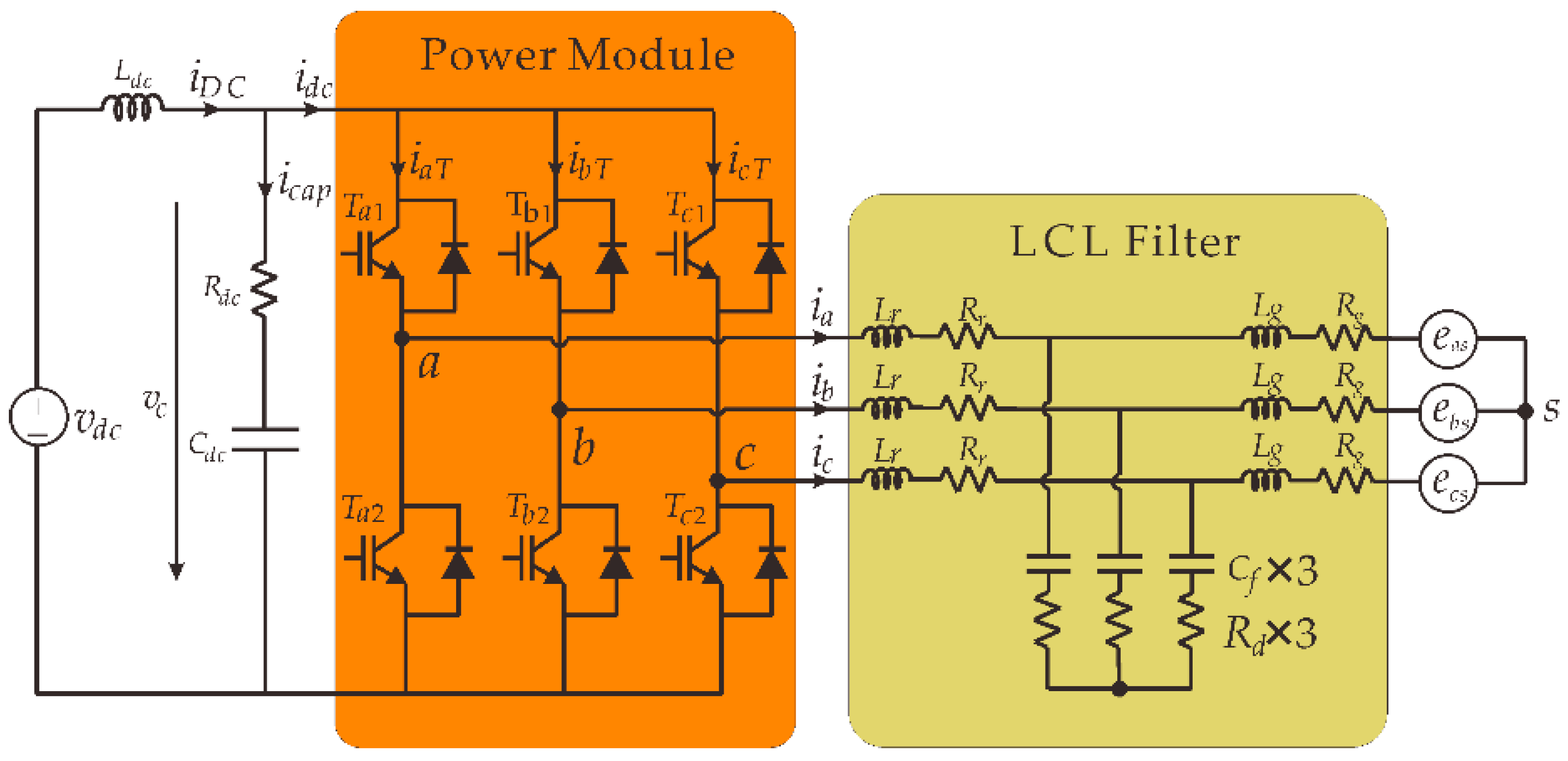
2.1. Basic Analysis of DC-Link Circuit
2.2. DC-Link Current Analysis
3. DC-Link Voltage Ripple
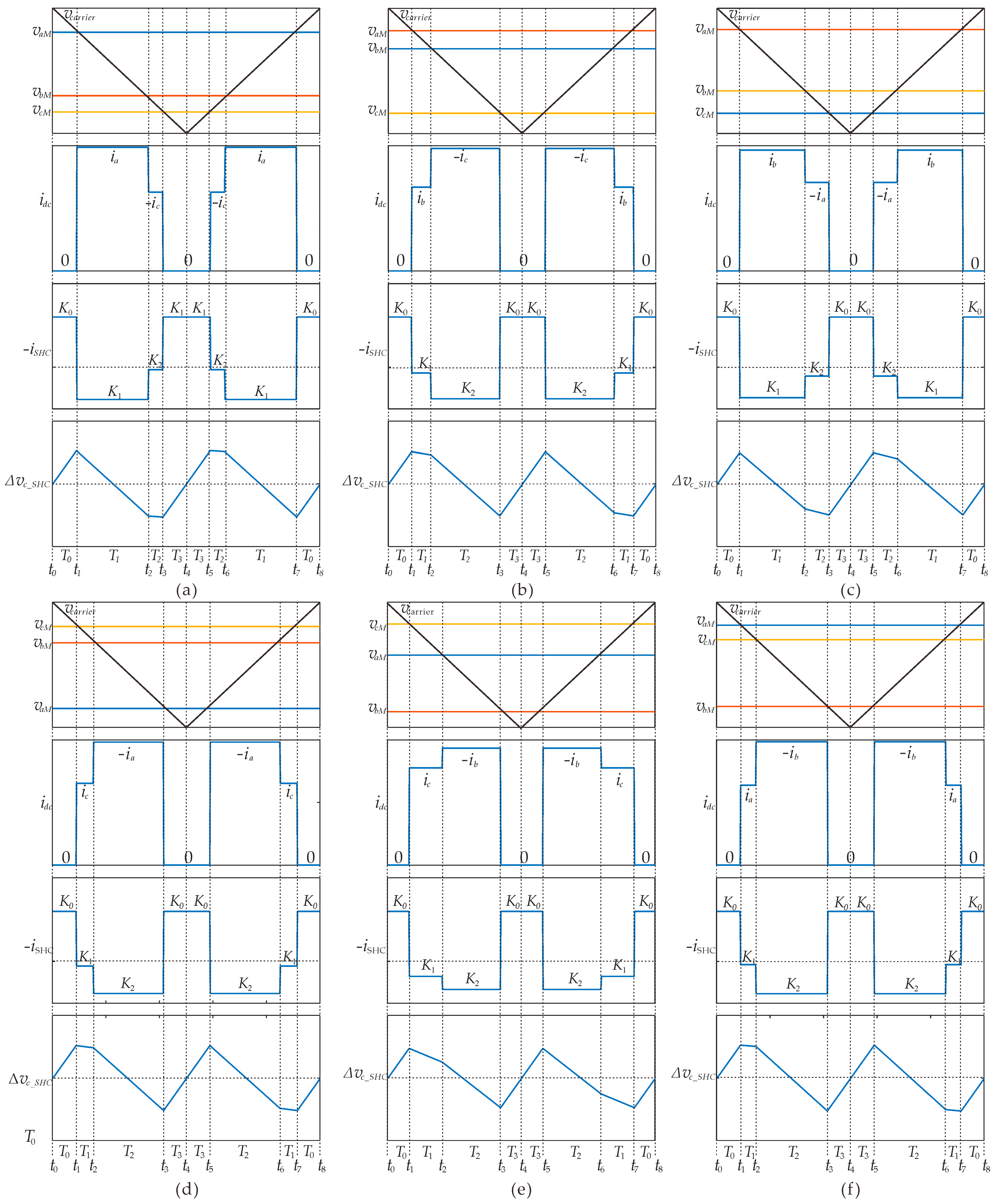
3.1. The LOH Voltage in DC-Link
3.2. The SHV in DC-Link
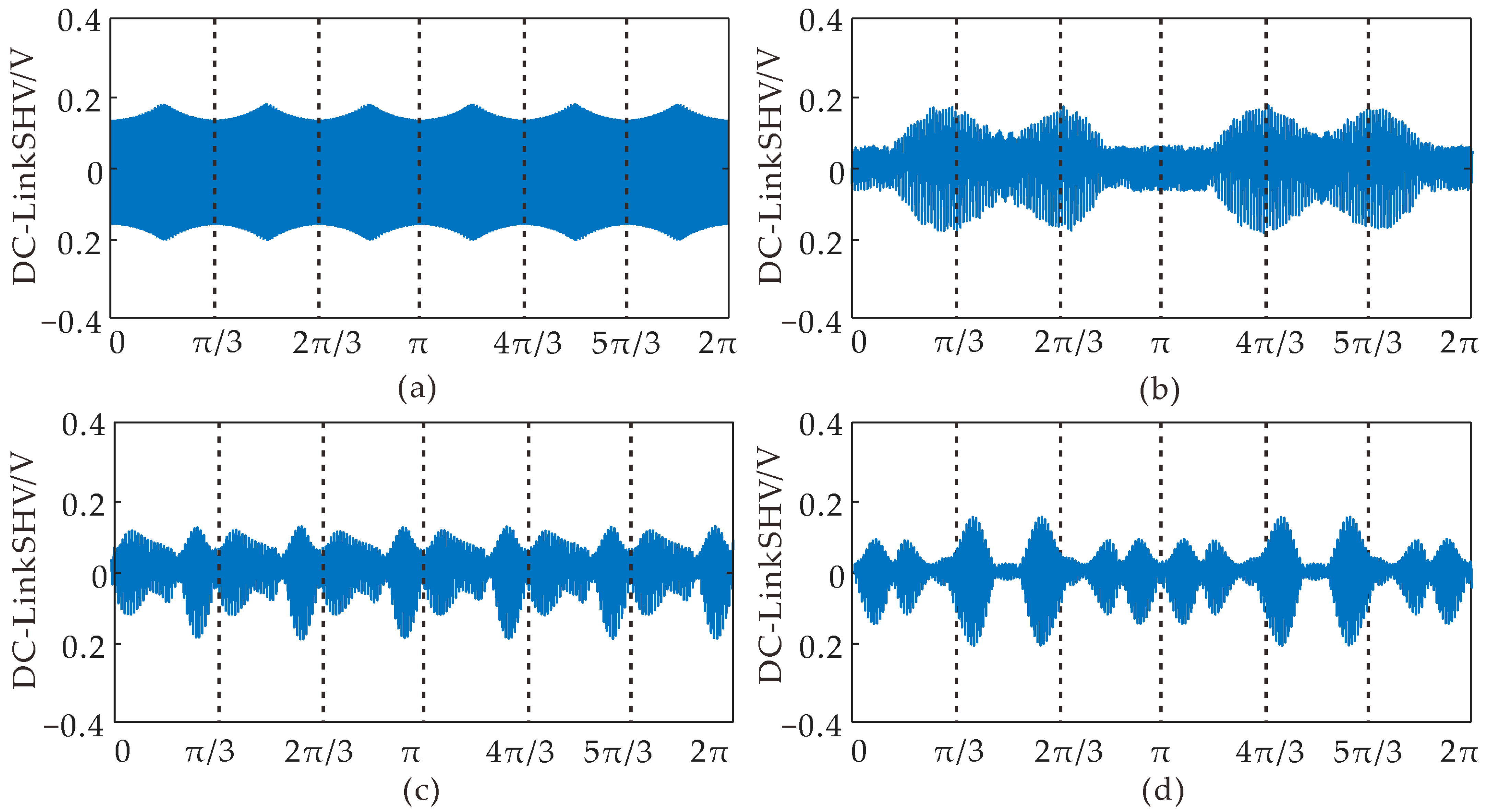
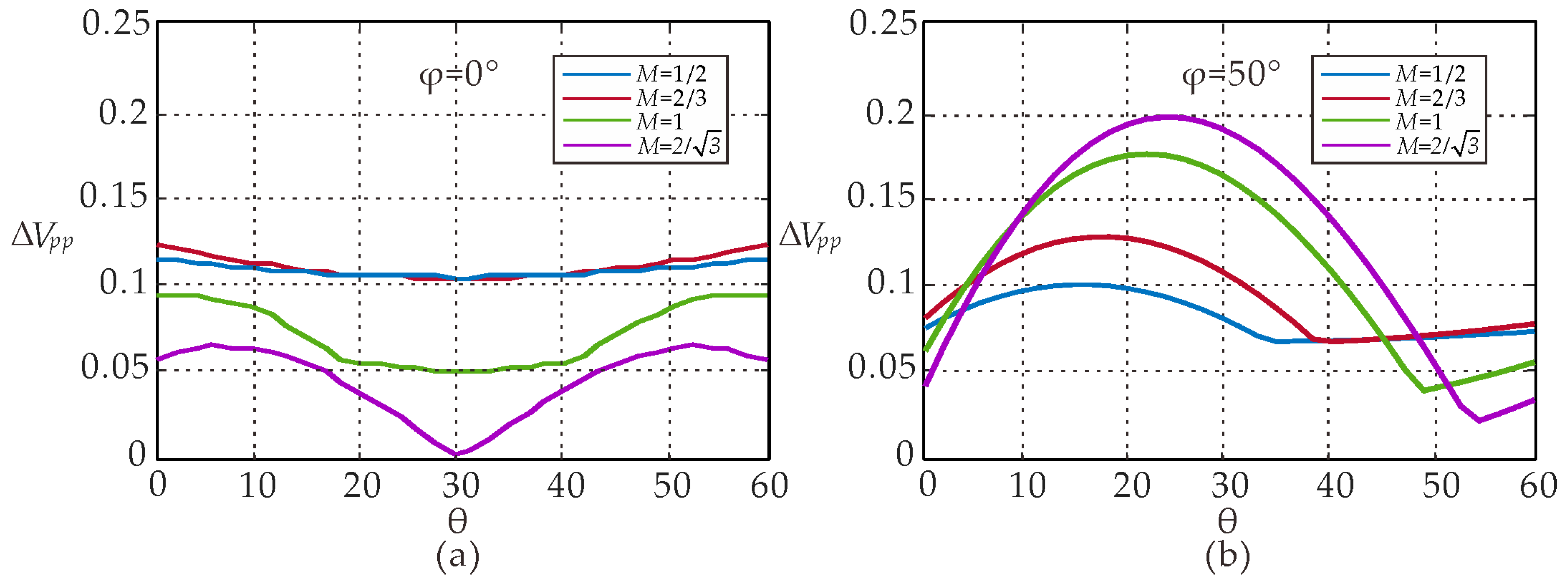
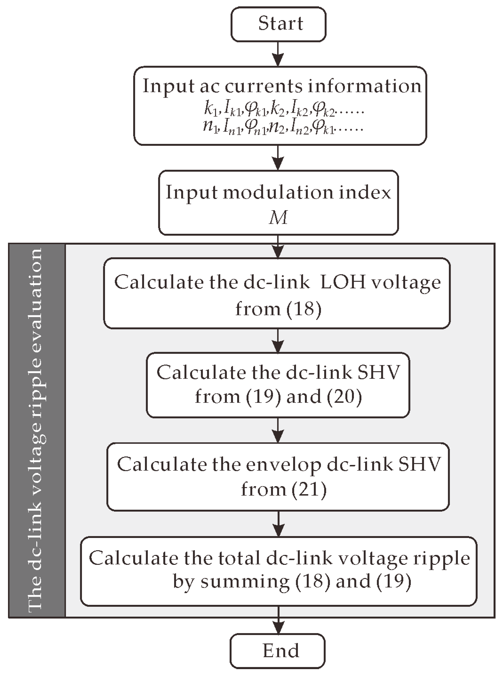
3.3. The DC-Link Voltage Ripple Evaluation
3.4. Equations Compatibility with Special Cases
3.5. Equations Simplification for Practical Design
4. Simulation and Experimental Results
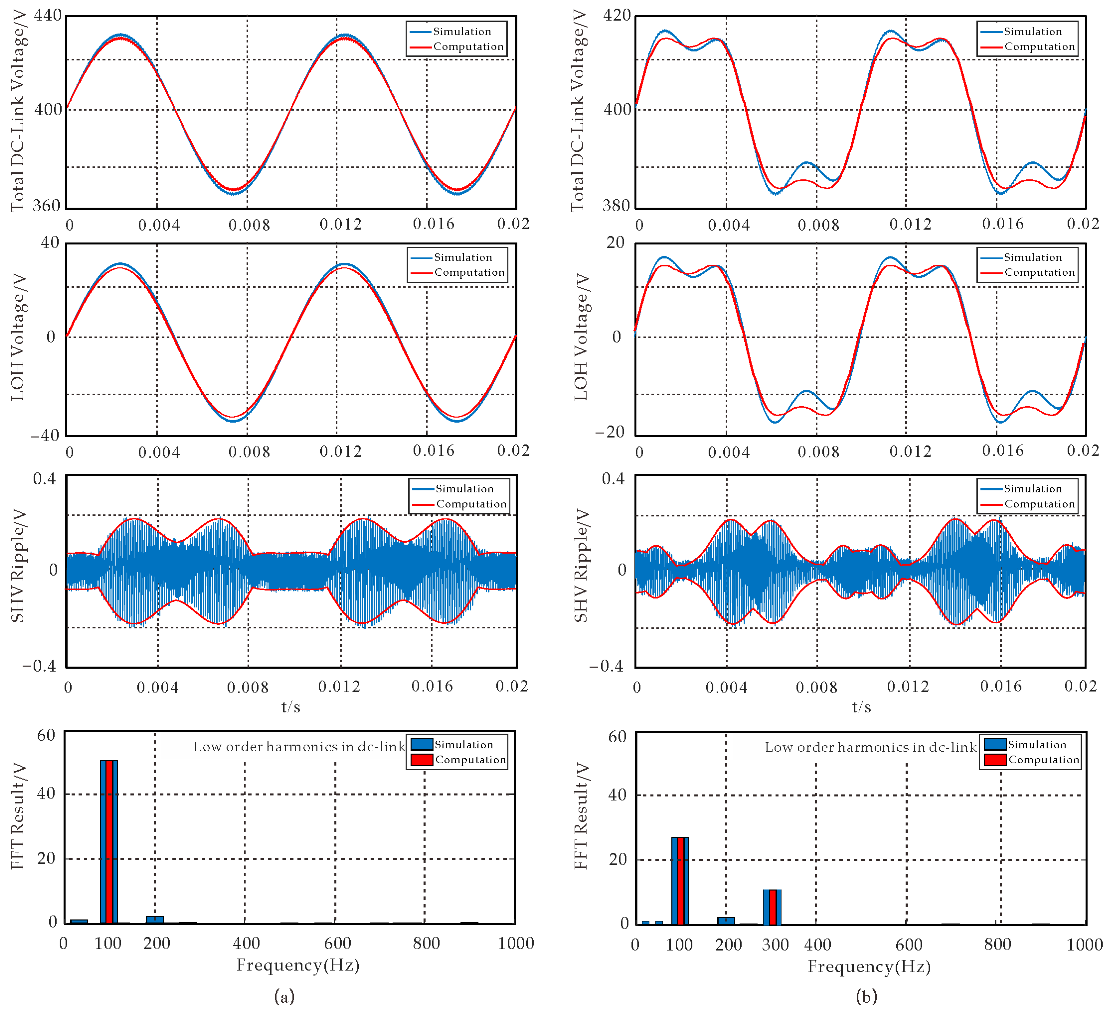
4.1. Simulation Results
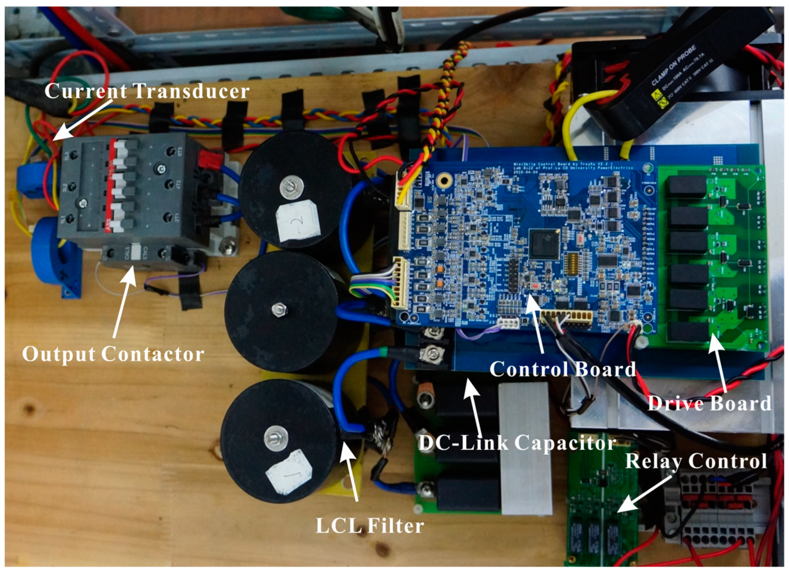
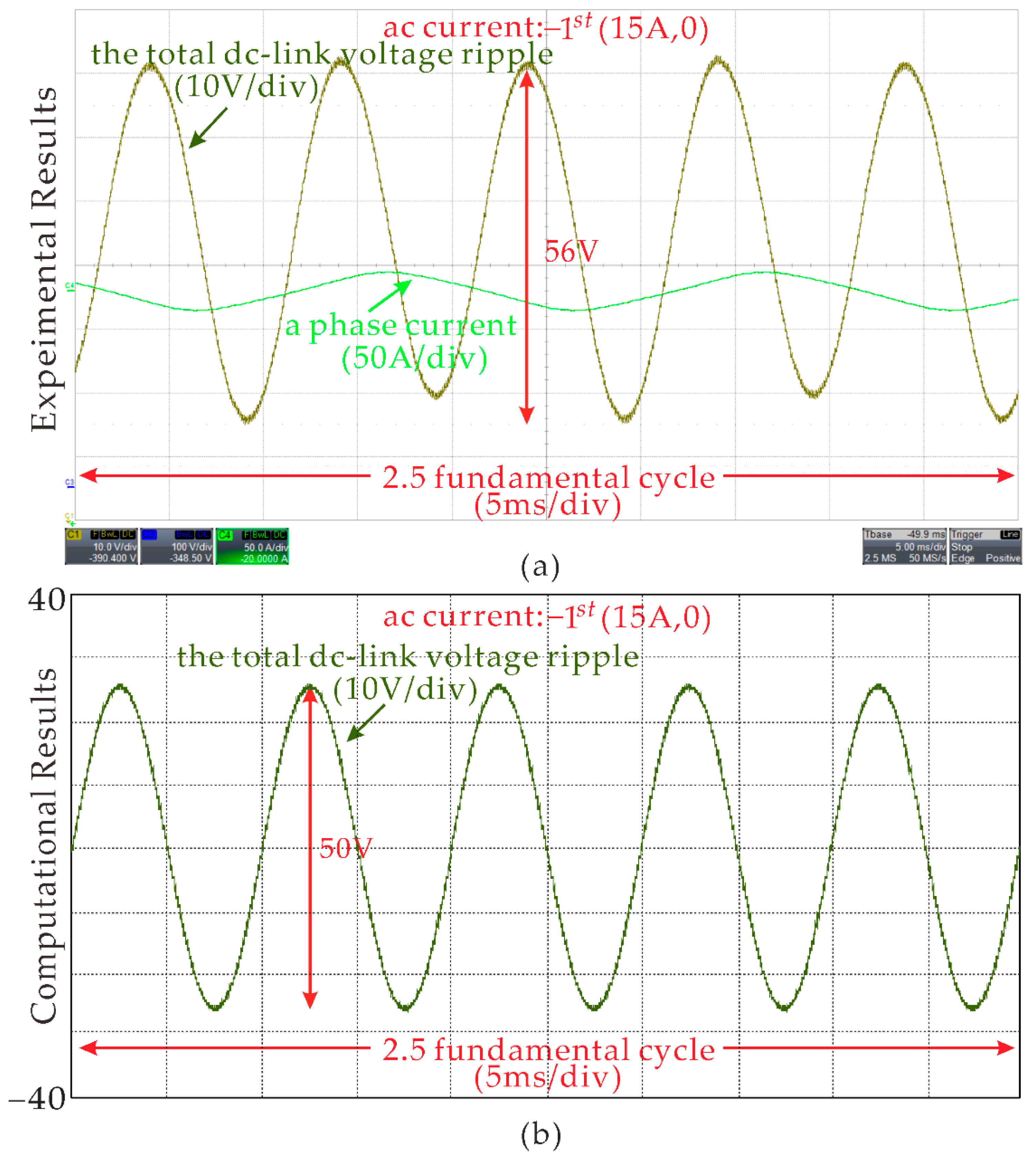
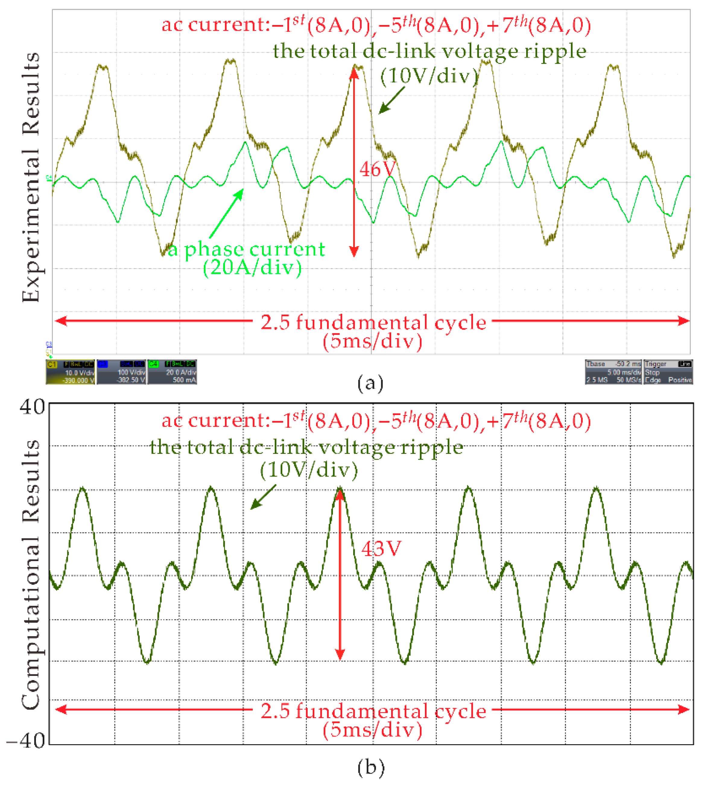
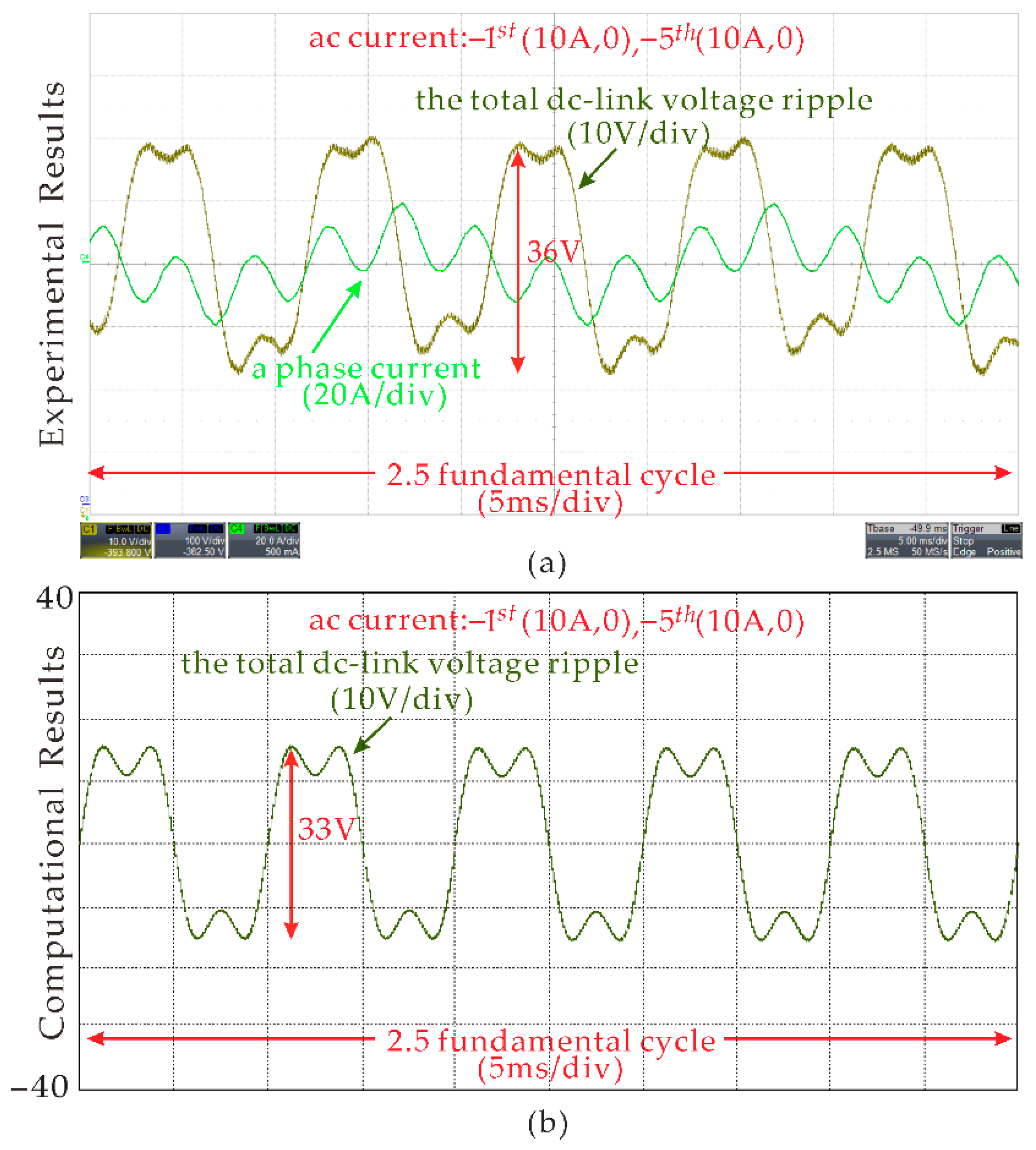
4.2. Experimental Results
5. Conclusions
Author Contributions
Funding
Institutional Review Board Statement
Informed Consent Statement
Data Availability Statement
Conflicts of Interest
References
- Bierhoff, M.H.; Fuchs, F.W. DC-Link Harmonics of Three-Phase Voltage-Source Converters Influenced by the Pulse width-Modulation Strategy—An Analysis. IEEE Trans. Ind. Electron. 2008, 55, 2085–2092. [Google Scholar] [CrossRef]
- McGrath, B.P.; Holmes, D.G. A General Analytical Method for Calculating Inverter DC-Link Current Harmonics. IEEE Trans. Ind. Appl. 2009, 45, 1851–1859. [Google Scholar] [CrossRef]
- Sun, J.; Lin, C. Calculation and spectral analysis of DC-link current for three phase PWM inverter. In Proceedings of the International Symposium on Power Electronics (Ee), Novi Sad, Serbia, 27–30 October 2021. [Google Scholar]
- Renken, F. Analytical calculation of the dc-link capacitor current for pulsed three-phase inverters. In Proceedings of the 11th International Conference on Power Electronics and Motion Control, Riga, Latvia, 2–4 September 2004. [Google Scholar]
- Kolar, J.W.; Round, S.D. Analytical calculation of the RMS current stress on the DC-link capacitor of voltage-PWM converter systems. IEEE Trans. Ind. Appl. 2006, 153, 535–543. [Google Scholar] [CrossRef] [Green Version]
- Ming, L.; Ding, W.; Loh, P.C.; Xin, Z. A Direct Carrier-Based Modulation Scheme With Full Index Range for DC-Link Current Ripple Mitigation of a Current Source Converter. IEEE Trans. Ind. Electron. 2022, 69, 452–462. [Google Scholar] [CrossRef]
- Nishizawa, K.; Itoh, J.; Odaka, A.; Toba, A.; Umida, H.; Fujita, S. Current Stress Reduction for DC-Link Capacitors of Three-Phase VSI With Carrier-Based Continuous PWM. IEEE Trans. Ind. Appl. 2019, 55, 6061–6072. [Google Scholar] [CrossRef]
- Dahono, P.A.; Sato, Y.; Kataoka, T. Analysis and minimization of ripple components of input current and voltage of PWM inverters. IEEE Trans. Ind. Appl. 1996, 32, 945–950. [Google Scholar] [CrossRef]
- Vujacic, M.; Hammami, M.; Srndovic, M.; Grandi, G. Theoretical and Experimental Investigation of Switching Ripple in the DC-Link Voltage of Single-Phase H-Bridge PWM Inverters. Energies 2017, 10, 1189. [Google Scholar] [CrossRef]
- Vujacic, M.; Hammami, M.; Srndovic, M.; Grandi, G. Analysis of dc-Link Voltage Switching Ripple in Three-Phase PWM Inverters. Energies 2018, 11, 471. [Google Scholar] [CrossRef] [Green Version]
- Pei, X.; Chen, C.; Kang, Y. Analysis of Voltage Ripple and Design for DC-Link Capacitor in Three-Phase Voltage Source Inverters. Trans. Electrotech. Soc. 2014, 29, 254–269. [Google Scholar]
- Vujacic, M.; Dordevic, O.; Grandi, G. Evaluation of DC-Link Voltage Switching Ripple in Multiphase PWM Voltage Source Inverters. IEEE Trans. Power Electron. 2020, 35, 3478–3490. [Google Scholar] [CrossRef]
- Guo, J.; Ye, J.; Emadi, A. DC-Link Current and Voltage Ripple Analysis Considering Antiparallel Diode Reverse Recovery in Voltage Source Inverters. IEEE Trans. Power Electron. 2018, 33, 5171–5180. [Google Scholar] [CrossRef]
- Pei, X.; Zhou, W.; Kang, Y. Analysis and Calculation of DC-Link Current and Voltage Ripples for Three-Phase Inverter With Unbalanced Load. IEEE Trans. Power Electron. 2015, 30, 5401–5412. [Google Scholar] [CrossRef]
- Wang, T.; Lu, S. Analysis of the DC-Link Current for the Single-Phase H-Bridge Inverter Under Harmonic Output Currents. IEEE J. Emerg. Sel. Top. Power Electron. 2019, 7, 2170–2183. [Google Scholar] [CrossRef]
- Wang, T.; Lu, S. DC-Link Current Computational Methods for Three Phase Inverter with Low Order Harmonic Output Current. IET Power Electron. 2019, 12, 878–890. [Google Scholar] [CrossRef]
- Yang, L.; Wang, T.; Li, S.; Liang, K.F. Analysis of the DC-link voltage ripple for the three phase voltage ripple under low order harmonic output current. In Proceedings of the International Conference on High Voltage Direct Current (HVDC), XJTU, Xi’an, China, 6–9 November 2020. [Google Scholar]


| Category | T0 | T1 | T2 | K0 | K1 | K2 |
|---|---|---|---|---|---|---|
| Sector 1 | Ts × (1 − uaref − ucom)/8 | Ts × (uaref − ubref)/4 | Ts × (ubref − ucref)/4 | idcLOH | idcLOH − ia | idcLOH + ic |
| Sector 2 | Ts × (1 − ubref − ucom)/8 | Ts × (ubref − uaref)/4 | Ts × (uaref − ucref)/4 | idcLOH | idcLOH − ib | idcLOH + ic |
| Sector 3 | Ts × (1 − ubref − ucom)/8 | Ts × (ubref − ucref)/4 | Ts × (ucref − uaref)/4 | idcLOH | idcLOH − ib | idcLOH + ia |
| Sector 4 | Ts × (1 − ucref − ucom)/8 | Ts × (ucref − ubref)/4 | Ts × (ubref − uaref)/4 | idcLOH | idcLOH − ic | idcLOH + ia |
| Sector 5 | Ts × (1 − ucref − ucom)/8 | Ts × (ucref − uaref)/4 | Ts × (uaref − ubref)/4 | idcLOH | idcLOH − ic | idcLOH + ib |
| Sector 6 | Ts × (1 − uaref − ucom)/8 | Ts × (uaref − ucref)/4 | Ts × (ucref − ubref)/4 | idcLOH | idcLOH − ia | idcLOH + ib |
| Category | Part Number | Parameters |
|---|---|---|
| Grid side inductor Lg | Custom-made | 200 uH, 30 Arms |
| Converter side inductor Lr | Custom-made | 400 uH, 40 Arms |
| Filter capacitor Cf | MKP1847610354P4 | 10 uF |
| Damping resistor Rd | TEH100M1R00JE | 1 Ω |
| DC-Link capacitor Cdc | 450HXG120MFM | 720 uF |
| IGBT modules | SKiiP 39AC126V2 | 1200 V |
Publisher’s Note: MDPI stays neutral with regard to jurisdictional claims in published maps and institutional affiliations. |
© 2022 by the authors. Licensee MDPI, Basel, Switzerland. This article is an open access article distributed under the terms and conditions of the Creative Commons Attribution (CC BY) license (https://creativecommons.org/licenses/by/4.0/).
Share and Cite
Li, S.; Yang, L.; Wang, T. Analysis of the DC-Link Voltage Ripple for the Three-Phase Voltage Source Converter under Nonlinear Output Current. Energies 2022, 15, 2892. https://doi.org/10.3390/en15082892
Li S, Yang L, Wang T. Analysis of the DC-Link Voltage Ripple for the Three-Phase Voltage Source Converter under Nonlinear Output Current. Energies. 2022; 15(8):2892. https://doi.org/10.3390/en15082892
Chicago/Turabian StyleLi, Shan, Lei Yang, and Tao Wang. 2022. "Analysis of the DC-Link Voltage Ripple for the Three-Phase Voltage Source Converter under Nonlinear Output Current" Energies 15, no. 8: 2892. https://doi.org/10.3390/en15082892
APA StyleLi, S., Yang, L., & Wang, T. (2022). Analysis of the DC-Link Voltage Ripple for the Three-Phase Voltage Source Converter under Nonlinear Output Current. Energies, 15(8), 2892. https://doi.org/10.3390/en15082892