Abstract
This paper elaborates on a development technique for the grid-connected voltage source converter (VSC). We propose a simulation technique in the MATLAB/Simulink environment that emulates the operation of the discrete-time controlled grid-connected VSC. The switched-circuit modeling approach is used for simulation of the power stage in the continuous-time domain with the physical unit scale. The discrete-time control algorithm is implemented in an interpreted MATLAB function in the per-unit scale, which synchronizes with the switching period. Such a control algorithm is easily translated into the C language for programing of the 32-bit C2000 DSP controller with the same regulators’ parameters. The proposed platform was validated with a hardware-in-the-loop real-time simulator and with a 5-kVA 3-phase LCL-filtered grid-connected VSC. The discrete-time control scheme was implemented in the synchronous reference frame control with proportional-integral with multi-resonant controllers at harmonic orders 6th and 12th for suppression of the grid voltage harmonic orders 5th, 7th, 11th, and 13th. The experimental results closely agreed with the simulation results. The experimental grid currents complied with the IEEE 1547 standard thanks to the multi-resonant controllers. The proposed platform provides a smooth transition from implementation to a near-commercial prototype with a low investment cost in simulation and rapid prototyping tools. A MATLAB/Simulink VSC model is provided as an attachment of this paper.
1. Introduction
Power electronic converters now play a vital role in modern electric power generation and distribution systems [1,2]. Three-phase voltage source converters (VSCs) are widely used to interlink DC and AC systems as illustrated in Figure 1. Common applications of the three-phase VSCs include photovoltaic [3] and wind energy systems [4], grid integration of battery storage systems [5], traction motor drives for transportation applications [6], and electric vehicle charging stations, etc. [7].
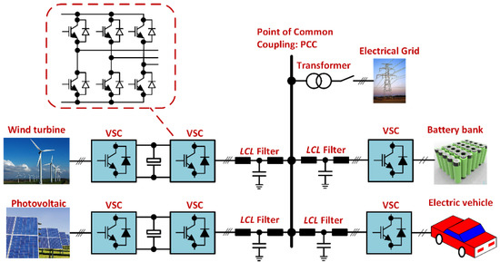
Figure 1.
Applications of VSCs in the electrical system.
Figure 2 illustrates the three-phase VSC structure where it can be divided into the power stage, switching signal generation, and discrete-time control system. The DC bus voltage control and the active/reactive power control are the outer control loops, which generate the reference grid current for the inner current control loop. The grid current is required to track the reference and to reject low-frequency harmonics in the grid voltage . Harmonic controllers are normally plugged into the fundamental component current controller. Multi-resonant controllers and repetitive controllers in the stationary reference frame , and multiple synchronous reference frame control are the common solutions for grid voltage harmonic mitigation. Moreover, frequency adaptation capability is required to maintain the control performance with the grid frequency variation. The duty ratios from the current control loop are sent to the pulse width modulation (PWM) unit to generate the switching signals for the semiconductor switches of the VSC. The control scheme of the three-phase VSCs and other power converters are now normally implemented on a microcontroller (µC) or a digital signal processor (DSP).
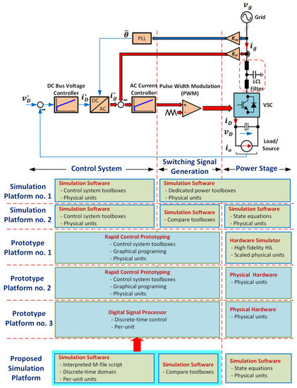
Figure 2.
Development platforms of the three-phase grid-connected VSC.
Development of a three-phase VSC starts from a simulation using power simulation software for the power stage, PWM, control systems such as PSIM or Simscape in MATLAB/Simulink (simulation platform 1 in Figure 2). This platform provides a quick validation before hardware prototyping. Component losses and thermal behavior can be easily modeled. However, a lack of deep knowledge in modeling the converter circuit and dynamic makes it difficult when designing the controllers. Moreover, the dedicated software cost is considerably high.
The power stage of the VSC can be simulated using the switched-circuit modeling technique [8] where the state equations are calculated for every switching state herein defined as simulation platform 2 in Figure 2. The semiconductors devices are normally considered as the ideal switches without voltage drops and switching and conducting losses. This technique can be modeled with basic blocks in MATLAB/Simulink. This switched circuit model can be easily connected with other control blocks that are already available in the Simulink. Investment cost in the software license is comparatively low. However, this method requires a deep understanding of the converter operation which takes additional time and effort compared with the simulation platform 1.
After computer simulation, the control scheme can be implemented into a rapid control prototyping (RCP) system, while the power stage of the VSC can be modeled in a hardware in the loop (HiL) system, defined as prototype platform 1 in Figure 2. RCP and HiL systems are normally equipped with field-programmable gate arrays (FPGAs) or high-performance microprocessors with digital and analog interfacing, which accelerates validation of the prototype. No programming effort is required since the control block diagrams in the simulation are directly translated into the RCP system. HiL systems provide high fidelity with a small-time step for real-time simulation of the semiconductor switches and passive components. It has been reported that the ratio of the switching period to the simulation time step should be greater than 60 times for equation-based modeling and 60,000 for physical-based modeling [9]. Common RCP systems for power electronic applications are dSPACE Microlabbox (Paderborn, Germany) [10,11] and OPAL-RT OP4510 (Montreal, QC, Canada) [12,13] and Imperix B-Box (Sion, Switzerland) [14] etc. Common commercial HiL systems are OPAL-RT OP4510 (Montreal, QC, Canada) [12], dSPACE SCALEXIO (Paderborn, Germany) [9], Typhoon HiL (Somerville, MA, USA) [15,16] and National Instruments LabVIEW FPGA (Austin, TX, USA) [17]. The VSC power stage emulated in a HiL system is easily connected with the control stage implemented in an RCP system or a DSP-based controller. Hardware simulation using HiL systems is normally used to validate control schemes for a large system such as a microgrid controller [18] or a high-power wind turbine converter [19].
The control scheme implemented in the RCP system can be connected to the physical hardware for the power converter, here defined as prototype platform 2 in Figure 2. This research platform is popular for quick verification of converter control methodologies, for which no programming effort is required. Physical units are virtually employed in such a system. Measured signals, i.e., voltages and currents are just scaled into the control block diagrams with their associated gains. Commercialization of prototype platform 2 takes further effort in the implementation of the control scheme. The control scheme is discretized and programmed onto a microcontroller or a DSP [20,21,22,23,24], here called prototype platform 3. The sampled currents and voltages are normally scaled into the per-unit (p.u.) system so that they are compatible with a limited numerical range of the DSP. This prototype platform 3 has a similar structure to commercial products for example power factor correction rectifiers, grid-connected inverters, and back-back converters [2,20,24]. Thus, it takes a little effort to commercialize the prototype platform 3.
Simulation platform 1 and prototype platforms 1 and 2 enable a smooth transition from modeling to implementation with a substantial investment in simulation software, RCP systems, and HiL systems. Alternatively, simulation platform 2 and prototype platform 3 are the cheapest development platforms, which are suitable for power converter research and development in developing countries. Example products and estimated costs of the simulation and prototype platforms are summarized in Table 1.

Table 1.
Example products and estimated cost for the simulation and prototype platforms.
This paper illustrates a development methodology for a DSP-based control power electronic converter that facilitates a smooth transition from implementation to a near-commercial prototype without a circuit-based simulation package and an RCP tool. This paper covers switched circuit modeling of the VSC, and its discrete-time control scheme developed in the MATLAB/Simulink environment from basic block diagrams. The control scheme is scaled into the per-unit system so that the regulators’ parameters can be directly transferred to the discrete-time control system implemented on a TMS320F28379D DSP controller from Texas Instruments (Dallas, TX, USA) as illustrated at the bottom of Figure 2. A three-phase grid-connected VSC with the proportional-integral plus multi-resonant (PIMR) controllers in the synchronous reference frame for mitigation of grid voltage harmonics is selected in this study. The proposed method was validated with a simulation platform 1 using the Simscape Electrical toolboxes in the MATLAB/Simulink, an HiL real-time simulator, and 5-kVA three-phase grid-connected VSC.
2. System Description
Figure 3 depicts an LCL-filtered three-phase grid-connected VSC with the synchronous reference frame control. The grid voltages, grid currents, and the DC bus voltage are sampled by the analog-to-digital converters (ADCs), which are represented as the zero-order hold (ZOH) blocks in the simulation. The sampled voltages are scaled by into the per-unit system and for the sampled currents. The superscript “ ´ ” denotes the signals in the p.u. scale. The grid currents are transformed to the synchronous reference frame, on which the -axes current and are regulated by the discrete-time current controllers with the reference current generated from the active power control loop and/or the DC bus voltage control loop and the reference current obtained from the reactive power control loop or by setting for a unity power factor. The distorted grid voltages , and are given by
where and is the grid frequency. The three-phase three-wire system contains the harmonic orders . A phase-locked loop (PLL) is used to estimate the grid voltage angle for the reference frame transformation. The grid voltage in the stationary reference frame is obtained from
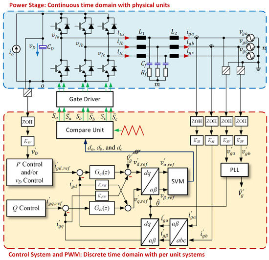
Figure 3.
Three-phase grid-connected LCL-filtered VSC with the discrete-time control scheme in the synchronous reference frame.
Note that the zero-sequence is neglected for the balanced system. Substituting (1) into (2), the grid voltage can be represented as
Thus, the grid voltage in the synchronous reference frame is given by
The voltage harmonic orders in the synchronous reference frame result from the harmonic orders in the stationary reference frame, which become the disturbances of the -axes current control loops. The PIMR controller depicted in Figure 4 is adopted for the -axes current regulators [25]. The PMR transfer function in the s-domain is given by
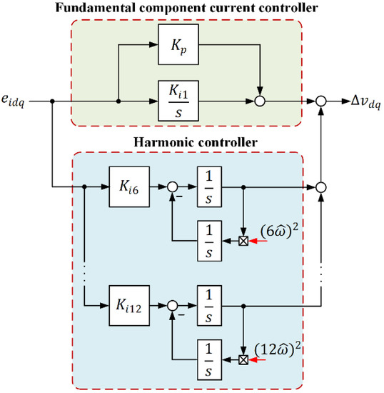
Figure 4.
Proportional-integral plus multi-resonant controller.
The proportional-integral (PI) controller regulates the fundamental component current which is the DC quantities in the -axes. The multiple resonant (MR) controllers regulate both negative and positive sequence components [26], which can be used to attenuate the grid voltage harmonics at the frequencies in the synchronous reference frame [25]. The double integrator structure of the resonant controllers uses the estimated grid frequency from the PLL for frequency adaptation. The equivalent transfer function of in the stationary reference frame is determined from [26].
Substitution of (5) into (6) becomes
The harmonic compensators in (7) are identical to individual resonant controllers tuned at frequencies in the stationary reference frame which is given by
Therefore, the stationary frame equivalence of the synchronous reference frame controller is similar to a proportional-multiple resonant controller implemented in the stationary reference frame [25], which is written by
The outputs of the -axes current controllers with feedforward of the decoupled terms form the VSC reference voltages and , which are converted to the stationary reference frame and using the inverse Park transformation given by
The reference voltages and are the inputs for the space vector modulation (SVM) which calculates the duty ratios , , and for the compare unit to generate the VSC switching commands.
The control scheme in Figure 3 is normally implemented on a DSP, and it must be executed within an interrupt service routine (ISR). Figure 5 illustrates the timing diagram of each ISR, which starts when the PWM carrier reaches zeros or the maxima. The controller sampling frequency doubles the switching frequency The analog signal sampling is synchronized with the ISR at time instance that occurs in the middle of the switching action to avoid switching noise. This requires a small filtering effort for each signal, which enhances the control loop bandwidth. The analog to digital conversion and scaling, and the PLL are executed every ISR. If the VSC operation is enabled, the other VSC control algorithms are performed, otherwise, they are skipped to the end of the ISR. The control scheme is executed within the sampling period , and the calculated duty ratios , , and are updated to the compare unit at the next time instance .

Figure 5.
Timing diagram and control sequence of the VSC discrete-time control.
The VSC currents , , and or the grid currents , , and can be used as the feedback signals for the current control loop. For the VSC current feedback, current sensors can be embedded in the VSC where overcurrent is directly protected. However, the injected power to the grid is not directly controlled. Moreover, the grid currents are susceptible to grid voltage harmonics [27]. Therefore, the grid currents are used for the feedback signals to directly control the injected power. The per-phase transfer function of the LCL filter is given by
This yields the resonant frequency of the LCL filter as
For the inherent damping, the sampling frequency and the resonant frequency of the LCL filter have to satisfy the stability criterion given by [28]
Table 2 lists the key parameters of the VSC and the LCL filter in this study. This LCL filter is inherited damped by the inductor winding resistances and , and the capacitor equivalent series resistance . This results in a resonant frequency of Hz which satisfies the stability criterion in (13). Passive, active, or hybrid damping techniques can be used to further improve control stability with the presence of large grid impedance [29].
Table 2.
Parameters of the VSC.
3. Modeling of the LCL-Filtered VSC
3.1. Switched Circuit Modeling of the Power Circuit
Figure 6 displays the equivalent circuit of the VSC. Resistors and are the winding resistance of the inductors and . Resistors are the equivalent series resistance of the capacitors plus the series damping resistance of the LCL filter. Resistor is the effective DC bus capacitance of the DC bus voltage sensor and the discharging resistor. The semiconductor switches are represented by switches , , and . The status of each switch is represented by “1” for the closed state and “0” for the opened state. The complementary switches , , and operate opposite , , and . Therefore, there are eight possible output states of the VSC. There are three reference points: , , and . The DC bus current is supplied or drawn by another converter, which is positive for the inverting mode and negative for the rectifying mode.

Figure 6.
Equivalent circuit of the three-phase grid-connected VSC with the LCL filter.
The grid currents , , and can be written as follows
where , , and are the voltages across the filter capacitor and the series resistor with respect to point , which are given by
The voltages across the filter capacitor , , , and are determined from
The VSC currents , , and are given by
where the VSC voltages , , and with respect to point depends on the switching states as follows
For the balanced three-phase three-wire system, ,, and , which results in
Thus, the grid currents can be written as follows
Adding the sub-equations of (17) together, the common mode voltage is expressed as
This common-mode voltage intrinsically exists in the two-level VSC due to limited switching states, which creates a leakage current through the parasitic capacitance between the DC bus and the neutral points of the system. The VSC currents , , and are driven by the differential mode voltages , , and between the VSC legs and the neutral point of the capacitor bank, which can be written as
The VSC DC current is written as
If the DC bus is connected to another converter buffered by the DC bus capacitor , the DC bus voltage is then modeled as
Figure 7a displays the VSC and LCL filter model developed in the MATLAB/Simulink environment, where (15), (16), (20), (22), and (23) are implemented. This model is valid when the DC bus voltage is greater than the peak value of the line-to-line grid voltage . The signal is used for the enable () and disable () VSC operation. If the VSC is disabled and , the VSC currents , , and are kept reset at zero. Meanwhile, the grid currents , , and circulate through , , , and . At the enable time , the switching signals , , and are enabled and the VSC is fully operated. Figure 7b shows the MATLAB/Simulink model of the DC bus voltage in (24), which is kept reset while the VSC is disabled. For the single-stage topology where the VSC is connected to a voltage source, the DC bus voltage equation in (24) is neglected.

Figure 7.
MATLAB/Simulink model: (a) the VSC and LCL filter; (b) the DC bus voltage.
3.2. Averaged Circuit Modeling and Current Controller Design
The frequency response of the LCL filter below its resonant frequency is similar to that of the L filter [30]. Moreover, the control bandwidth is selected below the resonant frequency of the LCL filter. Thus, the LCL filter can be approximated as the L filter for design of the current controller. The grid currents can be simplified as
where , . The VSC voltages are written by
According to (19) , the grid currents in (25) become
The variables in (26) are averaged over a sampling period for continuous-time domain approximation, which becomes
where the brackets ‘⟨ ⟩’ represent the variables averaged over . Equation (28) is scaled into the per-unit scale using the base voltage where is the base current and is the base impedance, which yields
where symbols ‘ ’ denotes variables in the per-unit scale, and and . The grid currents in (29) are transformed to the synchronous reference frame, axes, which results in
Figure 8 shows the equivalent control block diagram of the grid current in the synchronous reference frame with the per-unit scale. Note that the cross-coupling terms are due to the Park transformation, which can be decoupled in the control scheme. The delay terms represent the sampling delay caused by the digital control scheme and the transport delay caused by the PWM process, where for the double update rate PWM is shown in Figure 5 [31]. The decoupled terms leave the currents and are separately controlled. The PI regulator for the fundamental component current is initially designed in the continuous-time domain. The parameters for the resonant controllers are then selected in proportion to the integral gain . According to the design methodology in [31], the PI regulator parameters are selected as follows
where is the possible maximum cross-over frequency at a given phase margin . The cross-over frequency is given by
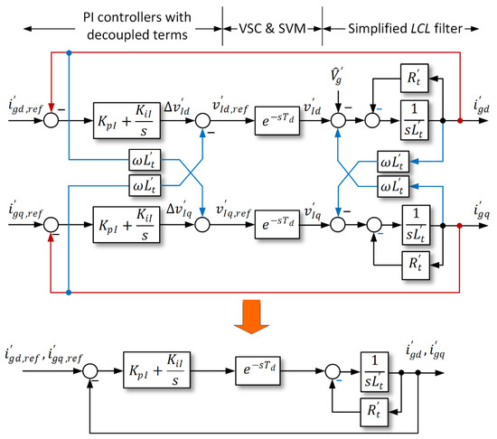
Figure 8.
Equivalent block diagram of the grid current in the synchronous reference frame.
Figure 9a shows the frequency response of the simplified open-loop transfer function with the PI controller and the PIMR controller. The target phase margin is set at with the VSC parameter in Table 1, which results in rad/s. The PI controller parameters and are determined from (31) and (32). The resonant controllers, orders 6th and 12th, are added to compensate the voltage harmonics, orders 5th, 7th, 11th, and 13th, whose resonant gains are set at . For the PI controller, the DC loop gain of 100 dB is large enough to track the reference currents with a zero steady-state error. However, the loop gains at 300 Hz and 600 Hz are considerably low to reject the voltage harmonic disturbances. For the PIMR controller, the DC loop gain and the loop gains at 300 Hz and 600 Hz are greater than 100 dB. The phase margin of the system with the PIMR controller is still large enough to guarantee the control stability. The actual cross-over frequency rad/s is close to the desired value.

Figure 9.
Frequency response of the current control loop: (a) simplified open-loop transfer function in synchronous reference frame with the PI controller (black) and the PIMR controller (red); (b) open-loop transfer function in the stationary reference frame.
The current controller is designed based on the simplified model. Stability assessment is necessary before implementation. The stationary reference frame equivalence of the current controller given in (9) and the transfer function of the LCL filter in (11) are used in the open-loop transfer function in the stationary reference frame which is written as
Figure 9b depicts the frequency response of in the stationary reference frame, where there are three cross-over frequencies , , and . The cross-over frequency near the loop bandwidth rad/s slightly shifts from that in the synchronous reference frame due to the presence of the 13th-harmonic peak gain. The phase margin at is still large enough to guarantee control stability. The other two cross-over frequencies rad/s and rad/s occur around the resonant frequency of the LCL filter , of which phase margins and satisfy the stability criterion for the inherent damping of the LCL filter with grid-current feedback control [28].
4. Simulation
4.1. Simulation Structure
Figure 10 shows the simulation model developed in the MATLAB/Simulink environment. The simulation model emulates the experimental system, which is divided into 2 sections: continuous-time domain and discrete-time domain. The continuous-time domain represents the three-phase grid and the VSC power circuits with the switching signals , , and as the inputs, where the switched-circuit model of the VSC and the LCL filter shown in Figure 7a is adopted. The single-stage topology is considered in this study where the DC bus voltage is supplied by a constant voltage source . The DC bus model in Figure 7b is neglected.

Figure 10.
MATLAB/Simulink model of the discrete-time controlled 3-phase grid-connected VSC.
The discrete-time domain section emulates the control scheme depicted in Figure 3. The grid voltages and , and grid currents and are scaled by the base voltage and base current . Then, they are sampled by the ZOHs at the time instance with the period of . This process represents the beginning of each ISR as shown in Figure 5. The discrete-time algorithms for PLL, reference frame transformations, -axes current control, and the continuous SVM [32] are written in a MATLAB m file, which is executed every sampling period by the interpreted MATLAB function block as shown in Figure 10. The outputs of this interpreted MATLAB function block are the duty ratios , , and , which are delayed by . This causes the duty ratios , , and to be updated at the time instance to compare with the triangular waveform. This waveform has the switching period similar to that in Figure 5, which emulates the PWM process in the DSP. Thus, the controller parameters used in the simulation can be directly transferred to the experimental system if they use the same base units. The variable-step solver ODE45 with the maximum step size of ns was selected in the Simulink setting. The proposed simulation model developed in the MATLAB/Simulink 2020b is provided in [33].
4.2. Discrete-Time Control Scheme
Figure 11 shows the Park-based PLL the discrete-time domain used for grid synchronization. The grid voltages , , and are transformed to the axes using the Clarke transformation. The Park transformation converts the grid voltages to the axes, and , which are cleaned by the low-pass filters with the constant for the distorted grid voltage. The integrator with a gain of the nominal grid frequency estimates the grid voltage angle for the Park transformation. The PI controller regulates the -axis voltage toward zero, which forces , , and The loop regulator is designed in the continuous-time domain using the symmetrical optimum (SO) method [34]. For simplicity, the low-pass filters and the PI regulators are discretized using the backward difference approximation because the sampling frequency is much greater than the PLL bandwidth. The coefficient for the low-pass filters in the discrete-time domain is given by
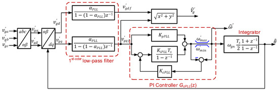
Figure 11.
Park-based phase-locked loop in the discrete-time domain for grid synchronization.
The saturation limit on the PI regulator output with an anti-windup is implemented through the correction gain which is usually twice the integral gain [35]. Meanwhile, the integrator for estimation of the grid voltage angle is discretized with the Tustin approximation with the lowest error. The estimated angle is then used for the axis transformations.
Figure 12 illustrates the discrete-time structure of the PIMR controller for control of the axes currents with the controller parameters obtained from the previous section. The PI controller for the fundamental component current is discretized using the backward difference approximation. Anti-windup is also implemented with the correction gain . For the resonant regulators, the forward difference approximation is used for the forward integrator, and the backward difference approximation is adopted for the feedback integrator [36]. This discretization technique is simple and does not create algebraic loops. The resonant frequency of the discrete controller is shifted from that in the continuous-time domain, especially at a higher frequency. However, it was analyzed in our previous work [37] that the shifted resonant frequency is marginal and creates an insignificant effect on the control performance. The two integrators can be discretized with the backward difference with an added one-step delay in the feedback path [36]. Discretization of both with the Tustin approximation causes a large shift of the resonant peak and poses implementation problems due to algebraic loops [36]. The resonant frequencies at the harmonic orders 6th and 12th are kept tuned with the estimated frequency from PLL for grid frequency adaptation. The fundamental current control has the intrinsic frequency adaptation capability through the Park transformation. Table 3 summarizes the parameters of the PLL and PIMR controller parameters.

Figure 12.
Discrete-time implementation of the PIMR controller.
Table 3.
Parameters of the discrete-time controllers.
5. Implementations
Figure 13 illustrates the experimental system. The power circuit was firstly modeled in an OPAL-RT OP4510 HiL real-time simulator with a time step of 220 ns to validate the discrete-time control scheme, which was implemented on a Texas Instruments TMS320F28379D 32-bit DSP controller as shown in Figure 13a. The emulated grid voltages and currents in the HiL system had the identical sensitivities to those used in the hardware implementation system as depicted in Figure 13b. A deadtime of 1 µs in each VSC leg was configured in the DSP. The VSC was constructed from Infineon IKW25T120 insulated-gate bipolar transistors (IGBTs) with isolated gate drivers from Texas Instruments ISO5851. Amorphous C cores (AMCC6.3 equivalence) were used for the construction of the inductors and of the LCL filter. The VSC was connected to a Chroma 61,860 60-kVA grid simulator. The DC bus was supplied to a Chroma 62150H-1000S DC power supply, 15 kW 0–1000 V, for the inverter operation. The discrete-time control scheme for the hardware implementation was identical to the HiL-based validation system. The ADC voltage range of this DSP is between 0 V to 3 V. Hall-effect current sensors, LEM HLSR 10-P/SP33, were used for measurement of the grid currents and . The grid voltage sensors were constructed from voltage divider circuits with AMC1200 isolation amplifiers. In this prototype, the line-to-line voltages and were measured, of which the instantaneous voltage vector was shifted by to be in the same angle with the instantaneous voltage vector of the phase voltage vector. A voltage reference, REF2030, provided a 1.50 V offset voltage for the grid current and grid voltage sensors.

Figure 13.
Experimental system of the three-phase VSC: (a) HiL-based implementation; (b) hardware implementation.
The measured voltages and currents were scaled into the per-unit system with the appropriate scaling factors as illustrated in Figure 14. In this example, a grid current with the peak value of is measured by a current sensor with the sensitivity of . An offset voltage is added to the sensor output to accommodate the 0- input range of the ADC, where is the maximum input voltage of the ADC, normally 3 V or 3.3 V. This translates to decimal values of 0 to , where is the ADC bit number. The ADC output that is equivalent in decimal is then normalized by . The offset is now equivalent to , which is subsequently removed in the software. The normalized signal with offset removal is multiplied by a scaling factor to have a unity amplitude at the base value. The numerical notation in the DSP can be in the signed fixed-point representation or the floating-point format. Scaling of the grid voltage has the same process as the grid current. No offset removal is required for the DC bus voltage, while the other procedures are similar to those of the grid voltage and current. In general, the signal scaling factor is given by

Figure 14.
Grid current conversion and scaling process for the experimental system.
The discrete-time control algorithm implemented in the MATLAB m file was manually translated to the C language for the DSP with the same controller parameters. Thus, the simulation and the experiment are closely related. However, there is a code generation tool for this DSP family with an additional licensing cost. The internal signals of the discrete-time control scheme implemented on the DSP were converted to 0–3.0 V analog signals via two embedded 12-bit digital-to-analog converters (DACs) for monitoring on an oscilloscope.
6. Simulation and Experimental Validations
The DC bus was connected to the Chroma 62150H-1000S DC power supply with V. The grid voltage waveforms were set to be sinusoidal at the nominal phase voltage of 230 V, 50 Hz. The PI controllers for the fundamental component were enabled without the harmonic compensators. The reference currents were set to p.u. and = 0 p.u. This caused the VSC to inject an active power of 5 kW into the grid. A simulation platform 1 of the VSC was developed in the Simscape Electrical of the MATLAB/Simulink 2020b, which is provided in [33]. Figure 15 compares the experiment and simulation results for the VSC-side currents , , and , and the grid currents , , and . It can be observed the experimental VSC-side currents , , and of the HiL and hardware implementations have the current envelops due to the switching in close agreement with those of the proposed simulation method and the simulation platform 1. This confirms that the switched circuit modeling technique is applicable for the proposed platform. The waveforms of the experimental and simulation grid currents , , and are near sinusoidal as the LCL filter absorbs the switching current ripples.
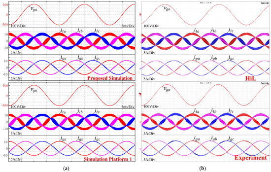
Figure 15.
Simulation and experimental results of the VSC without the harmonic compensators under the sinusoidal voltages: (a) Proposed simulation method and simulation platform 1; (b) HiL-based experiment and hardware implementation.
Voltage harmonics listed in Table 4 were added to the fundamental component, which resulted in a total harmonic distortion (THD) of 4.69%. Figure 16 shows the grid voltages and the grid currents without the harmonic compensators (HC). The experimental results from the HiL and hardware implementations closely agree with the proposed simulation method and simulation platform 1. The grid voltage harmonics make the grid currents even more distorted with a THD of 10.84%. The PIMR controller was adopted for control of the VSC under the distorted grid. The PIMR controller is capable of mitigating the grid voltage distortion as depicted in Figure 17. The grid current waveforms in the steady state are near sinusoidal. The control performance is maintained when the frequency changes from 47 Hz to 50 Hz and from 50 Hz to 52 Hz through the estimated frequency from the PLL. This is the allowable frequency range for a VSC connected to the Thailand low-voltage grid [38]. Figure 18 compares the current harmonic spectrum of the VSC at the nominal power of 5 kW under the distorted grid voltage. For the PI controller without the HCs, the current harmonics, orders 5th and 7th, exceed the IEEE 1547 standard [39] and there is a significant presence of orders 11th and 13th, which reflects the grid voltage harmonics. Moreover, the 2nd harmonic current also exceeds the IEEE 1547 standard, which is believed to be due to DC offsets in the current measurement [40]. The PIMR controller effectively suppresses the grid voltage harmonics as the current harmonic orders 5th, 7th, 11th, and 13th are attenuated close to zero. The grid current with the PIMR controller has a THD of 1.08% and complies with the IEEE 1547 standard.
Table 4.
Line-neutral voltage harmonics.

Figure 16.
Simulation and experimental results of the VSC without the harmonic compensators under the distorted voltages.
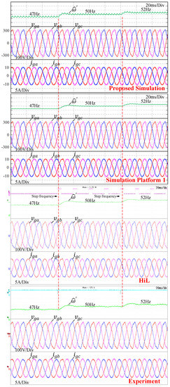
Figure 17.
Simulation and experimental results of the VSC with the PIMR controller under the distorted voltages and frequency changes.

Figure 18.
Current harmonic spectrum of the VSC at the nominal power of 5 kW under the distorted grid.
Dynamic performance of the VSC with the PIMR control scheme was validated with step changes in the reference currents as shown in Figure 19. The reference currents are initially set to p.u. and = 0 p.u.; the reference currents are changed to p.u. and = 0 p.u., and p.u., respectively. The experimental results of the grid currents at the steady-state conditions again are close to the proposed simulation method and simulation platform 1. The rising slope of the experimental and for the HiL and hardware implementations at the step changes of the reference currents as circled in Figure 19 are slightly lower than that of the simulation. This is believed to be due to voltage drops in the IGBTs and the grid simulator’s internal impedance, which were neglected in the simulation.
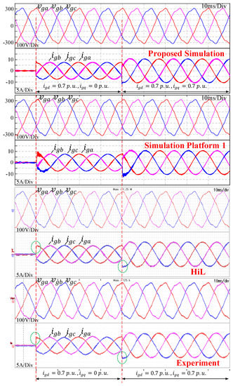
Figure 19.
Transient performance of the VSC with the PIMR controller.
It is demonstrated that the proposed simulation technique mimics the converter and control scheme very closely. The results of the proposed simulation technique closely agreed with the results of the simulation platform 1 using the Simscape Electrical toolboxes in the MATLAB/Simulink 2020b, and with the experimental results of the HiL and hardware implementations. The discrete-time control scheme implemented in the interpreted MATLAB function can be easily translated to the C-code for the DSP, from which expensive RCP systems and Simulink coding toolboxes are not required. Furthermore, a HiL simulator is not necessary for the development of a low-power VSC (say up to 20 kW). This platform can be applied to other topologies. Our previous works in interleaved DC-DC converters [41], single-phase stand-alone inverter [42], and single-phase grid-connected VSCs [37,43] were developed using the proposed platform. However, validation of the control scheme with a HiL simulator or a laboratory-scale VSC is a normal practice for the development of a large power converter.
7. Conclusions
We propose a simulation technique that emulates the DSP-based control operation of the grid-connected converters. The key features of the proposed platform can be listed as follows.
- Switched-circuit modeling of the power circuit is simulated in the continuous-time domain with the physical unit scale.
- The discrete-time control scheme in the per-unit scale is written in a MATLAB m file function which is executed in synchronous with the switching period.
- The m-file script is then easily translated to the C code for the TMS320F28379D DSP with the same controller parameters.
The proportional-integral with multi-resonant controllers at harmonic orders 6th and 12th in the synchronous reference frame was selected in the study to attenuate the grid voltage harmonics. The proposed platform was validated with an OPAL-RT OP4510 HiL real-time simulator and with 5-kVA 3-phase LCL-filtered grid-connected VSC. The experimental results from the HiL simulator and the VSC closely agree with the simulation. The multi-resonant controllers were found to effectively suppress the grid voltage harmonic orders 5th, 7th, 11th, and 13th with the THD of 4.69%. The grid current was found to comply with the IEEE 1547 standard with the THD of 1.08%. The proposed platform requires a basic package of MATLAB/Simulink without dedicated power electronic toolboxes and real-time prototyping systems.
Author Contributions
Conceptualization, S.S. (Sakda Somkun), P.Z., U.K., J.T., D.A. and M.P.; methodology, S.S. (Suparak Srita); validation, S.S. (Suparak Srita); formal analysis, S.S. (Suparak Srita); investigation, S.S. (Suparak Srita); resources, S.S. (Sakda Somkun); data curation, S.S. (Suparak Srita), T.K.; writing—original draft preparation, S.S. (Suparak Srita), and S.S. (Sakda Somkun); writing—review and editing, S.S. (Suparak Srita), and S.S. (Sakda Somkun); visualization, S.S. (Suparak Srita); supervision, S.S. (Sakda Somkun); project administration, S.S. (Sakda Somkun); funding acquisition, W.R. All authors have read and agreed to the published version of the manuscript.
Funding
This research was funded by Naresuan University, grant number R2563C026.
Institutional Review Board Statement
Not applicable.
Informed Consent Statement
Not applicable.
Data Availability Statement
The MATLAB/Simulink models presented in this study are available in “Srita, S.; Somkun, S. 3-Phase LCL-Filtered Grid-Connected VSC Modeling; Mendeley Data: 2022. https://doi.org/10.17632/xbpchksg3k.1 (accessed on 1 February 2022)”.
Acknowledgments
Many thanks to PTS combination Co., Ltd., for providing an OPAL-RT OP4510 HiL FPGA real-time simulator used in this study. Suparak Srita is grateful to the Energy Policy and Planning Office (EPPO), Ministry of Energy, Thailand for sponsoring his doctoral study.
Conflicts of Interest
The authors declare no conflict of interest.
Nomenclature
| ADC | Analog-to-digital converter |
| DAC | Digital-to-analog converter |
| DSP | Digital signal processor |
| FPGA | Field-programmable gate array |
| HC | Harmonic controller |
| HiL | Hardware in the loop |
| IGBT | Insulated-gate bipolar transistor |
| ISR | Interrupt service routine |
| MR | Multiple resonant |
| PI | Proportional-integral |
| PIMR | Proportional-integral plus multi-resonant |
| PLL | Phase-locked loop |
| PWM | Pulse width modulation |
| RCP | Rapid control prototyping |
| SO | Symmetrical optimum |
| SVM | Space vector modulation |
| VSC | Voltage source converter |
| ZOH | Zero-order hold |
| µC | Microcontroller |
| , and | Duty ratios |
| Sampling frequency | |
| Switching frequency | |
| Resonant frequency of the LCL filter | |
| VSC DC current | |
| , , and | Grid currents |
| , , and | VSC currents |
| DC bus current | |
| , , and | VSC switching signals |
| PWM delay time | |
| Sampling period | |
| Switching period | |
| DC bus voltage | |
| , and | LCL filter voltages |
| , and | Grid voltages |
| , and | VSC terminal voltages |
| Angle of the grid voltage | |
| Phase margin | |
| Grid angular frequency | |
| Cross-over frequency | |
| Nominal grid angular frequency | |
| Subscripts | |
| and | Signals in the synchronous reference frame |
| Refence signals | |
| and | Signals in the stationary reference frame |
| Superscripts | |
| Signals in the per unit scale | |
| Symbols | |
| Peak value or estimated value | |
| averaged variables over |
References
- Huang, Z.; Krishnaswami, H.; Yuan, G.; Huang, R. Ubiquitous Power Electronics in Future Power Systems: Recommendations to Fully Utilize Fast Control Capabilities. IEEE Electrif. Mag. 2020, 8, 18–27. [Google Scholar] [CrossRef]
- Chen, M.; Poor, H.V. High-Frequency Power Electronics at the Grid Edge: A Bottom-Up Approach Toward the Smart Grid. IEEE Electrif. Mag. 2020, 8, 6–17. [Google Scholar] [CrossRef]
- Patel, N.; Kumar, A.; Gupta, N.; Ray, S.; Babu, B.C. Optimised PI-4VPI current controller for three-phase grid-integrated photovoltaic inverter under grid voltage distortions. IET Renew. Power Gener. 2020, 14, 779–792. [Google Scholar] [CrossRef]
- Jahanpour-Dehkordi, M.; Vaez-Zadeh, S.; Mohammadi, J. Development of a Combined Control System to Improve the Performance of a PMSG-Based Wind Energy Conversion System Under Normal and Grid Fault Conditions. IEEE Trans. Energy Convers. 2019, 34, 1287–1295. [Google Scholar] [CrossRef]
- Peña Asensio, A.; Gonzalez-Longatt, F.; Arnaltes, S.; Rodríguez-Amenedo, J.L. Analysis of the Converter Synchronizing Method for the Contribution of Battery Energy Storage Systems to Inertia Emulation. Energies 2020, 13, 1478. [Google Scholar] [CrossRef] [Green Version]
- Grasso, E.; Palmieri, M.; Mandriota, R.; Cupertino, F.; Nienhaus, M.; Kleen, S. Analysis and Application of the Direct Flux Control Sensorless Technique to Low-Power PMSMs. Energies 2020, 13, 1453. [Google Scholar] [CrossRef] [Green Version]
- Sun, Q.; Lv, H.; Gao, S.; Wei, K.; Mauersberger, M. Optimized Control of Reversible VSC with Stability Mechanism Study in SMES Based V2G System. IEEE Appl. Supercond. 2019, 29, 1–6. [Google Scholar] [CrossRef]
- Maksimovic, D.; Stankovic, A.M.; Thottuvelil, V.J.; Verghese, G.C. Modeling and simulation of power electronic converters. Proc. IEEE 2001, 89, 898–912. [Google Scholar] [CrossRef]
- Chakraborty, S.; Mazuela, M.; Tran, D.; Corea-Araujo, J.A.; Lan, Y.; Loiti, A.A.; Garmier, P.; Aizpuru, I.; Hegazy, O. Scalable Modeling Approach and Robust Hardware-in-the-Loop Testing of an Optimized Interleaved Bidirectional HV DC/DC Converter for Electric Vehicle Drivetrains. IEEE Access 2020, 8, 115515–115536. [Google Scholar] [CrossRef]
- Adib, A.; Mirafzal, B.; Wang, X.; Blaabjerg, F. On Stability of Voltage Source Inverters in Weak Grids. IEEE Access 2018, 6, 4427–4439. [Google Scholar] [CrossRef]
- Xin, Z.; Wang, X.; Loh, P.C.; Blaabjerg, F. Grid-Current-Feedback Control for LCL-Filtered Grid Converters With Enhanced Stability. IEEE Trans. Power Electron. 2017, 32, 3216–3228. [Google Scholar] [CrossRef]
- Almaguer, J.; Cárdenas, V.; Espinoza, J.; Aganza-Torres, A.; González, M. Performance and Control Strategy of Real-Time Simulation of a Three-Phase Solid-State Transformer. Appl. Sci. 2019, 9, 789. [Google Scholar] [CrossRef] [Green Version]
- Chauhan, S.; Singh, B. Control of solar PV-integrated battery energy storage system for rural area application. IET Renew. Power Gener. 2021, 15, 1030–1045. [Google Scholar] [CrossRef]
- Taul, M.G.; Wu, C.; Chou, S.F.; Blaabjerg, F. Optimal Controller Design for Transient Stability Enhancement of Grid-Following Converters Under Weak-Grid Conditions. IEEE Trans. Power Electron. 2021, 36, 10251–10264. [Google Scholar] [CrossRef]
- Sener, E.; Ertasgin, G. Current-source 1-Ph inverter design for aircraft applications. Aircr. Eng. Aerosp. Technol. 2020, 92, 1295–1305. [Google Scholar] [CrossRef]
- Duran, M.F. Digital Control of a Renewable Energy Resource Interfacing the Distribution Grid. Master’s Thesis, Escola Tècnica Superior d’Enginyeria Industrial de Barcelona, Barcelona, Spain, 2018. [Google Scholar]
- Estrada, L.; Vázquez, N.; Vaquero, J.; De Castro, Á.; Arau, J. Real-Time Hardware in the Loop Simulation Methodology for Power Converters Using LabVIEW FPGA. Energies 2020, 13, 373. [Google Scholar] [CrossRef] [Green Version]
- Nigam, S.; Ajala, O.; Dominguez-Garcia, A.D. A Controller Hardware-in-the-Loop Testbed: Verification and Validation of Microgrid Control Architectures. IEEE Electrif. Mag. 2020, 8, 92–100. [Google Scholar] [CrossRef]
- Salgado-Herrera, N.M.; Campos-Gaona, D.; Anaya-Lara, O.; Medina-Rios, A.; Tapia-Sánchez, R.; Rodríguez-Rodríguez, J.R. THD Reduction in Wind Energy System Using Type-4 Wind Turbine/PMSG Applying the Active Front-End Converter Parallel Operation. Energies 2018, 11, 2458. [Google Scholar] [CrossRef] [Green Version]
- Zhu, D.; Zou, X.; Zhao, Y.; Peng, T.; Zhou, S.; Kang, Y. Systematic controller design for digitally controlled LCL-type grid-connected inverter with grid-current-feedback active damping. Int. J. Electr. Power Energy Syst. 2019, 110, 642–652. [Google Scholar] [CrossRef]
- Samanes, J.; Urtasun, A.; Gubia, E.; Petri, A. Robust multisampled capacitor voltage active damping for grid-connected power converters. Int. J. Electr. Power Energy Syst. 2019, 105, 741–752. [Google Scholar] [CrossRef]
- Said-Romdhane, M.B.; Naouar, M.W.; Belkhodja, I.S.; Monmasson, E. An Improved LCL Filter Design in Order to Ensure Stability without Damping and Despite Large Grid Impedance Variations. Energies 2017, 10, 336. [Google Scholar] [CrossRef] [Green Version]
- Rodriguez-Diaz, E.; Freijedo, F.D.; Vasquez, J.C.; Guerrero, J.M. Analysis and Comparison of Notch Filter and Capacitor Voltage Feedforward Active Damping Techniques for LCL Grid-Connected Converters. IEEE Trans. Power Electron. 2019, 34, 3958–3972. [Google Scholar] [CrossRef] [Green Version]
- Aravena, J.; Carrasco, D.; Diaz, M.; Uriarte, M.; Rojas, F.; Cardenas, R.; Travieso, J.C. Design and Implementation of a Low-Cost Real-Time Control Platform for Power Electronics Applications. Energies 2020, 13, 1527. [Google Scholar] [CrossRef] [Green Version]
- Liserre, M.; Teodorescu, R.; Blaabjerg, F. Multiple harmonics control for three-phase grid converter systems with the use of PI-RES current controller in a rotating frame. IEEE Trans. Power Electron. 2006, 21, 836–841. [Google Scholar] [CrossRef]
- Teodorescu, R.; Blaabjerg, F.; Liserre, M.; Loh, P.C. Proportional-resonant controllers and filters for grid-connected voltage-source converters. IEE Proc. Electr. Power Appl. 2006, 153, 750–762. [Google Scholar] [CrossRef] [Green Version]
- Xin, Z.; Mattavelli, P.; Yao, W.; Yang, Y.; Blaabjerg, F.; Loh, P.C. Mitigation of Grid-Current Distortion for LCL-Filtered Voltage-Source Inverter With Inverter-Current Feedback Control. IEEE Trans. Power Electron. 2018, 33, 6248–6261. [Google Scholar] [CrossRef]
- Wang, J.; Yan, J.D.; Jiang, L.; Zou, J. Delay-dependent stability of single-loop controlled grid-connected inverters with LCL filters. IEEE Trans. Power Electron. 2016, 31, 743–757. [Google Scholar] [CrossRef] [Green Version]
- Wu, W.; Liu, Y.; He, Y.; Chung, H.S.; Liserre, M.; Blaabjerg, F. Damping Methods for Resonances Caused by LCL-Filter-Based Current-Controlled Grid-Tied Power Inverters: An Overview. IEEE Trans. Ind. Electron. 2017, 64, 7402–7413. [Google Scholar] [CrossRef] [Green Version]
- Dannehl, J.; Wessels, C.; Fuchs, F.W. Limitations of Voltage-Oriented PI Current Control of Grid-Connected PWM Rectifiers With LCL Filters. IEEE Trans. Ind. Electron. 2009, 56, 380–388. [Google Scholar] [CrossRef]
- Holmes, D.G.; Lipo, T.A.; Mcgrath, B.P.; Kong, W.Y. Optimized design of stationary frame three phase AC current regulators. IEEE Trans. Power Electron. 2009, 24, 2417–2426. [Google Scholar] [CrossRef]
- Holmes, D.G.; Lipo, T.A. Pulse Width Modulation For Power Converters Principles and Practice; IEEE Press: Manhattan, NY, USA, 2003. [Google Scholar]
- Srita, S.; Somkun, S. 3-Phase LCL-Filtered Grid-Connected VSC Modeling. Mendeley Data. 2022. Available online: https://data.mendeley.com/datasets/xbpchksg3k/1 (accessed on 1 February 2022).
- Golestan, S.; Freijedo, F.D.; Guerrero, J.M. A Systematic Approach to Design High-Order Phase-Locked Loops. IEEE Trans. Power Electron. 2015, 30, 2885–2890. [Google Scholar] [CrossRef] [Green Version]
- Åström, K.J.; Hägglund, T. PID Controllers: Theory, Design, and Tuning, 2nd ed.; ISA: Research Triangle Park, NC, USA, 1995. [Google Scholar]
- Yepes, A.G.; Freijedo, F.D.; Doval-Gandoy, J.; Lopez, O.; Malvar, J.; Fernandez-Comesana, P. Effects of discretization methods on the performance of resonant controllers. IEEE Trans. Power Electron. 2010, 25, 1692–1712. [Google Scholar] [CrossRef]
- Somkun, S. High performance current control of single-phase grid-connected converter with harmonic mitigation, power extraction and frequency adaptation capabilities. IET Power Electron. 2021, 14, 352–372. [Google Scholar] [CrossRef]
- Provicial Electricity Authority, Provincial Electricity Authority’s Regulation on the Power Network System Interconnection Code. 2016. Available online: https://www.pea.co.th/Portals/0/Document/vspp/PEA%20Interconnection%20Code%202016.pdf (accessed on 1 February 2022).
- IEEE Std 1547–2018 (Revision of IEEE Std 1547–2003); IEEE Standard for Interconnection and Interoperability of Distributed Energy Resources with Associated Electric Power Systems Interfaces; IEEE: Manhattan, NY, USA, 2018; pp. 1–138. [CrossRef]
- Trinh, Q.N.; Wang, P.; Tang, Y.; Koh, L.H.; Choo, F.H. Compensation of DC Offset and Scaling Errors in Voltage and Current Measurements of Three-Phase AC/DC Converters. IEEE Trans. Power Electron. 2018, 33, 5401–5414. [Google Scholar] [CrossRef]
- Somkun, S.; Sirisamphanwong, C.; Sukchai, S. A DSP-based interleaved boost DC-DC converter for fuel cell applications. Int. J. Hydrogen Energy 2015, 40, 6391–6404. [Google Scholar] [CrossRef]
- Somkun, S. Unbalanced synchronous reference frame control of singe-phase stand-alone inverter. Int. J. Electr. Power Energy Syst. 2019, 107, 332–343. [Google Scholar] [CrossRef]
- Somkun, S.; Chunkag, V. Unified unbalanced synchronous reference frame current control for single-phase grid-connected voltage-source converters. IEEE Trans. Ind. Electron. 2016, 63, 5425–5436. [Google Scholar] [CrossRef]
Publisher’s Note: MDPI stays neutral with regard to jurisdictional claims in published maps and institutional affiliations. |
© 2022 by the authors. Licensee MDPI, Basel, Switzerland. This article is an open access article distributed under the terms and conditions of the Creative Commons Attribution (CC BY) license (https://creativecommons.org/licenses/by/4.0/).