Article

High-Voltage Isolated Multiple Output Auxiliary Power Supply with Output Voltage Self-Regulation

Institute of Power Electronics and Electric Traction, School of Electrical Engineering, Beijing Jiaotong University, Beijing 100044, China
*
Author to whom correspondence should be addressed.
Energies 2022, 15(6), 2106; https://doi.org/10.3390/en15062106
Submission received: 10 January 2022 / Revised: 10 March 2022 / Accepted: 11 March 2022 / Published: 13 March 2022

Abstract

:
Power electronic transformers (PETs) have high voltage isolation requirements and a large number of modules, which requires the auxiliary power supply (APS) to achieve high voltage isolation and multiple outputs. This paper proposes a parameter optimization method for the current source APS applied to PETs, enabling the APS to have multiple output voltage self-regulation capabilities. By optimizing the excitation inductance and leakage inductance for the current transformer of the APS, the excitation current plays a regulating role in energy transmission, thus realizing the self-regulation of the output voltages. The proposed method enables the voltage deviation and voltage change of the output modules to be suppressed under the unbalanced loads and large load fluctuations. Moreover, the APS can still operate normally when a short-circuit or an open-circuit fault occurs on the output sides. Therefore, the stability and reliability of the APS are improved, and the design difficulty of the post-stage voltage regulator circuit is also reduced. Finally, the simulation results are given, and a prototype containing three output modules was built to verify the effectiveness of the proposed parameter optimization method.

1. Introduction

The controllers, drivers, sensors, system protection circuits, and monitoring circuits of the power converters need to be powered by the auxiliary power supply (APS), which is isolated from the main circuit of the power converters. Therefore, the APS is the basis to ensure the normal startup, operation, and protection of the power converters [1,2,3].
Modular series-parallel technology, limited by the withstand voltage and insulation capabilities of existing power semiconductors, is usually adopted by power electronic transformers (PETs), which reduces the voltage and current stress of each switching device and the power level of each sub-module [4,5,6,7,8]. Therefore, PETs usually have a large number of sub-modules. Take PETs and DC transformers as an example; for a PET in the three-phase 10 kV power grid, if 3.3 kV IGBT is used to construct the H-bridges of PET, at least 6 sub-modules connected in series are required [8]; for a DC transformer with an input voltage of 20 kV, if a 1.7 kV IGBT is used, 25 serial sub-modules are required [9]. How to safely and reliably supply the controllers, drivers, and sensors of each sub-module is a crucial issue to be considered in the design process of PETs [8,9,10,11,12].
According to the characteristics of PETs, the factors that need to be considered in the design process of APS can be summarized: (1) high voltage isolation between the input and output sides of the APS and between the multi-outputs is required; (2) the APS needs to provide multiple independent outputs; (3) to ensure the stability of the APS, it is necessary to ensure that the multi-outputs of the APS are stable within the preset voltage range under different load powers; (4) APS can maintain stable operations in abnormal conditions, such as short-circuit or open-circuit faults, occur on the output sides.
Some voltage source APS topologies were proposed in [13,14,15,16], including an inverter and isolated converter. The inverter, which is in the front stage of the APS, converts the DC voltage into an AC voltage, and the output side of the inverter is connected to the voltage bus. A high voltage high-frequency plasma switching power supply was presented in [17]. The full-bridge PWM topology was developed as an inverter to convert the DC voltage into a high frequency pulsating DC output voltage. However, the inverter could not achieve soft switching, which increased the losses of the inverter to some extent. The isolated converters, which are on the output side of the APS, are connected in parallel to the voltage bus and take power from the voltage bus. The isolated converters are independent and output a DC voltage to supply the auxiliary electrical equipment of the power converters (controllers, drivers, sensors, etc.). The voltage source type APS topologies require an isolation transformer with multiple turns for each isolated converter and a separate controller for each output. Due to the insulation and isolation requirements of the PETs for the isolation transformers, the volume and cost of the isolation transformers can be very high. Therefore, the voltage source type APS topologies are unsuitable for PETs. An isolation transformer based on a coreless PCB structure was proposed in [18] to meet high voltage isolation requirements. The voltage isolation capability of this particular structure was mainly determined by the insulation properties of the PCB board. Due to structural constraints, this topology cannot provide multiple outputs. In [19], a piezoelectric transformer was proposed, which implemented high voltage isolation utilizing the electrical energy-mechanical energy-electric energy conversion. This structure could only provide a single output, and the modulation and demodulation of the signal undoubtedly increased the system complexity. To meet the high voltage isolation requirements and provide multiple outputs, reference [20] proposed a two-stage isolation APS topology. The first stage, an isolated DC-DC converter with single-input single-output, was used to achieve high voltage isolation. The second stage was a single input multiple output structure to meet the needs of multiple outputs. However, the output modules of this topology were not isolated from each other, and the number of output modules was very limited.
The current source APS topology was proposed in [21,22,23], consisting of a current source, inverter circuits, current transformers, and rectifier bridges. The front stage current source and inverter converted the input DC voltage into an AC current source. The current transformers played the role of high voltage isolation and energy transmission, and the rectifier bridges convert the alternating current into direct current. A toroidal core was used in the isolation transformer, and a single insulated cable passed through all the magnetic rings as the primary winding of each current transformer. The current transformer can obtain high-voltage isolation capability if a high-voltage cable is used in the primary winding. In this power supply structure, the number of magnetic rings can be easily adjusted so that multiple outputs can be realized easily. Based on these advantages, the current source APS can meet the power supply requirements of PETs. However, these power supply schemes did not solve the problems that the APS works abnormally due to the significant voltage deviation or fluctuation among output modules under unbalanced load, large load fluctuation, short circuit, and open circuit fault of output modules. Based on [22], the parameter design method of the current transformer was described in [23]. However, the parameter optimization method was not further proposed, and the problems mentioned above were not be solved. Based on [24], a resonant network was added between the inverter and the current transformer [25], which improved the performance of the power supply to a certain extent, such as output current THD, efficiency, and anti-interference ability. However, the solution also failed to solve the reliability problems under the unbalanced load power, large load fluctuation, open circuit, or short circuit fault of the output module. A thyristor short circuit was proposed in [26] at the post-stage of the rectifier bridge to deal with the open circuit. However, this method inevitably increased the complexity of the whole system. Besides, the scheme did not propose corresponding solutions for the unbalanced load and large load fluctuations.
Given that the current source APS cannot normally work under the unbalanced loads, large load fluctuations, open circuit and short-circuit fault of the output module, etc., a parameter design method is proposed in this paper, which can effectively improve the reliability and stability of APS under the above conditions. The key to the parameter design method is to design the excitation inductance and leakage inductance of the current transformer so that the excitation current of the current transformer can play a regulating role in the energy transmission process. The parameter-optimized APS obtain output voltage self-regulation characteristics; that is, the output voltage change of the APS under the conditions mentioned above can be suppressed, and no voltage regulation control strategy is required. The proposed parameter design method enables the APS to maintain a small voltage deviation for each output module under unbalanced load power conditions and significant load fluctuation. In the case of short-circuit or open-circuit failure of the output module, the APS can maintain the normal operation.
This paper is organized as follows: Section 2 introduces the topology of the proposed APS and the basic working principle of the parameter-optimized APS. In Section 3, the output voltage self-regulation of the APS is studied, and the parameter design method is proposed. Moreover, the output voltage self-regulation characteristic of the parameter-optimized APS is verified through simulation analysis. In Section 4, the experiments verified the feasibility and effectiveness of the proposed parameter design method. Finally, the conclusions of this paper are drawn in Section 5.

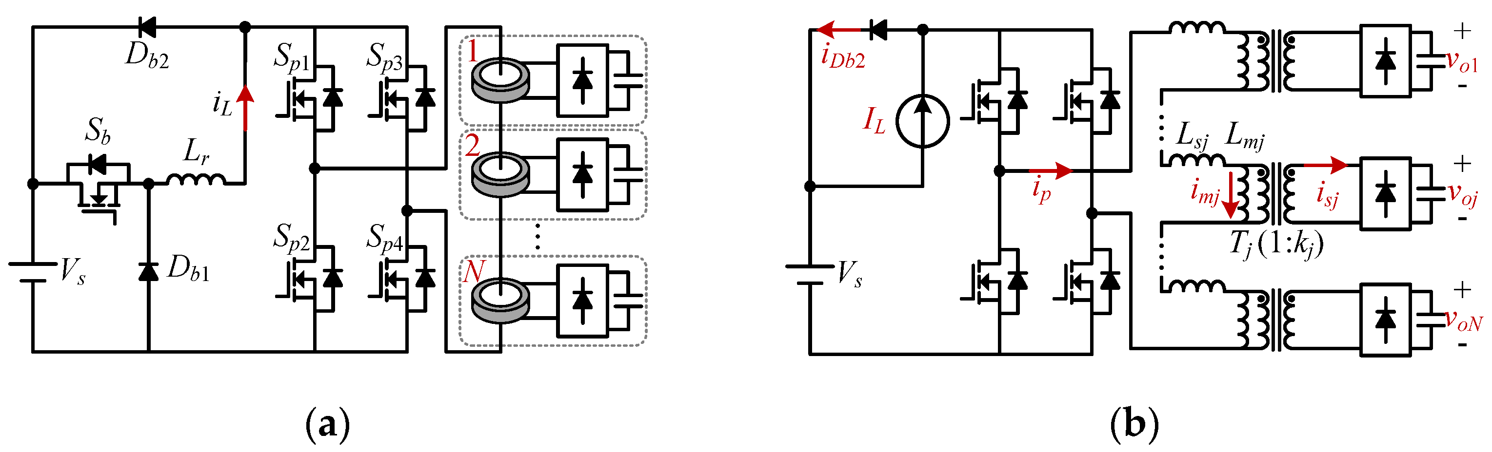
2. Topology and Principle

2.1. Topology

The commonly used current source APS topology and equivalent circuit are shown in Figure 1, which is mainly composed of four parts: a current source converter, an inverter circuit, current transformers, and rectifier bridges. According to the power supply requirements, voltage regulators can be connected at the post-stage of the rectifier bridges to obtain a standard voltage. Power diodes Db1, Db2, switching device Sb, and filter inductor Lr constitute the current source converter, converting the input DC voltage into a DC current. The inverter, which converts the DC current source into an AC current source, is composed of switch devices Sp1Sp4. The current transformer in the APS uses a toroidal core. A high-voltage insulated cable is used to pass all the magnetic rings as the primary winding of all the current transformers, and several turns of cables wound on each magnetic ring as the secondary winding of the current transformer. After rectifying and filtering the current on the secondary side of the current transformer, an isolated power supply can be obtained.

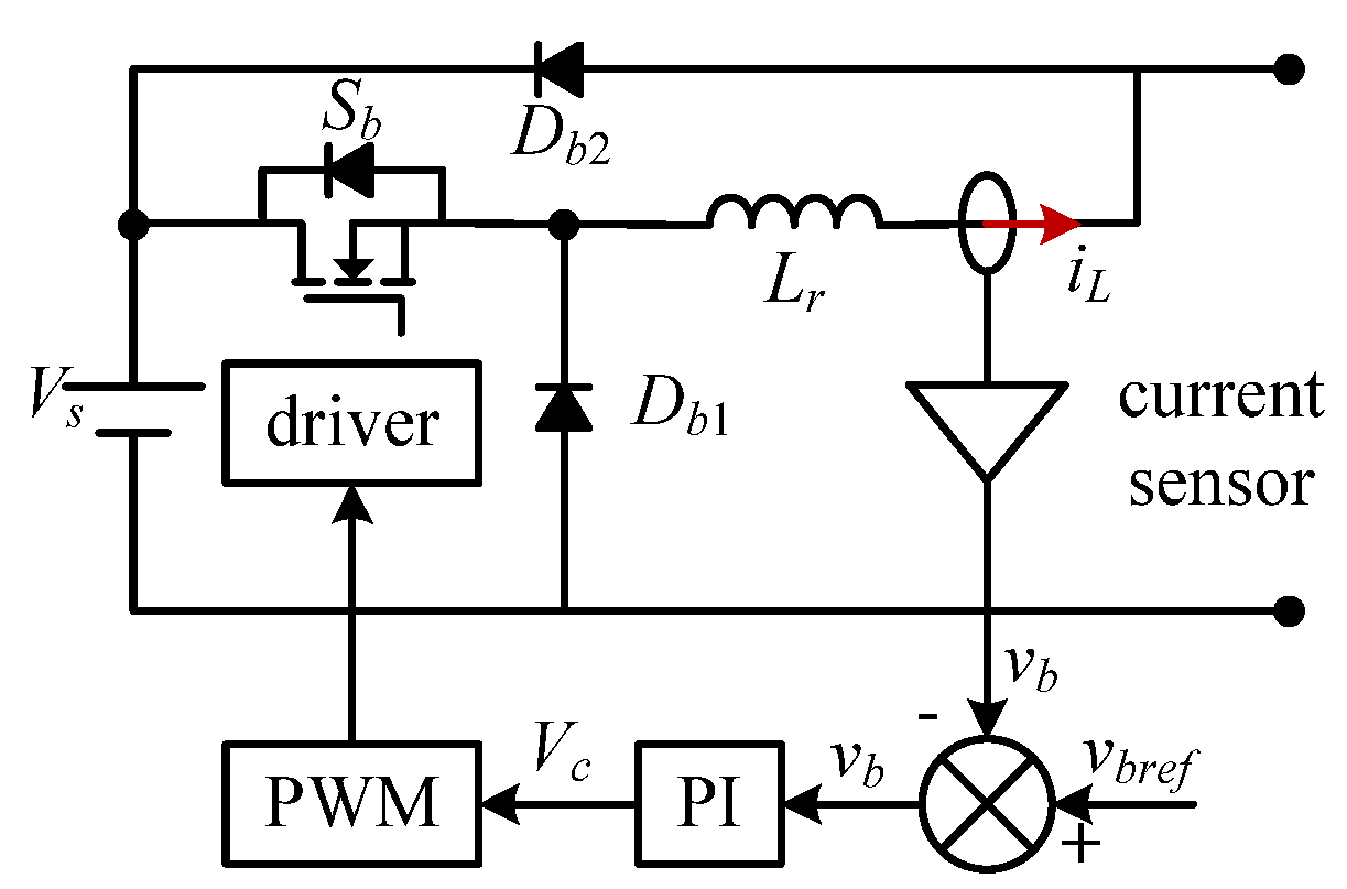
2.2. Basic Principle

Compared with the existing current source APS scheme, this paper proposes a parameter design method to optimize the parameters of the current transformer so that the APS has the characteristics of output voltage self-regulation. The magnetizing inductance is usually large for the commonly used transformer, so the magnetizing current is often so small that it can be ignored. In the proposed APS scheme, the excitation inductance is specially designed so that the excitation current can play a regulating role in the power transmission process of the current transformer.
The control diagram of the current source converter is shown in Figure 2. The PWM controller is used in the current source converter. The current sensor collects the current signal of filter inductor iL and converts the current signal into voltage signal vb. The voltage signal vb is compared with the reference voltage signal vbref, and the controller adjusts the comparison result to obtain a modulated voltage signal. Then the modulated voltage signal is sent to the comparator to obtain the pulse signal, which is sent to the driving circuit to control the switching operation of the switching devices. Under different load conditions, the current of filter inductor iL is kept constant by adjusting the duty cycle of the Sb, and the adjustment range of the duty cycle of the switching device is 0–1.
A fixed pulse drives the switching devices of the inverter with a 50% duty cycle. The switching devices Sp1, Sp4 are turned on and off synchronously, and their on–off state is complementary to the switching devices Sp2, Sp3. The control circuit of the current source converter and the inverter are independent of each other. There is no coupling between the current source converter and the inverter, so coordinated control is not required.
This paper analyzes the basic working principle of the APS after parameter optimization. The theoretical waveform of the APS after the parameter optimization is shown in Figure 3. The following assumptions are made to simplify the analysis of the basic principle of the APS:
  • The input and output voltages are all ideal DC voltages, and the effects of voltage ripple are not considered;
  • The switching ripple of the filter inductor current iL is small enough so that the current source converter is regarded as an ideal current source and iL is equal to IL.
As shown in Figure 3, the APS has eight working intervals in one switching cycle, corresponding to eight working modes. The analysis of each operating mode is as follows.
Mode I (t0t1): at the initial moment, the primary current of the current transformer is the same as the excitation current, and its value is equal to the negative value of the filter inductor current; that is, ip(t0) = imj(t0) = −IL (j = 1, 2, …, N, which represents the j th output module in APS. N is the total number of output modules). At t0, Sp2, and Sp3 are turned off, so the primary current of the current transformer ip flows through the anti-parallel diodes of the Sp1 and Sp4. ip is superimposed with the filter inductor current and then feedback to the input voltage source via Db2. At the same time, the input voltage source begins to transfer energy to the output side. The secondary current of the current transformer can be obtained by subtracting the primary current and the excitation current. The primary current ip(t) of the current transformers, the excitation current imj(t), and secondary current isj(t) of the j th current transformer can be expressed as
i p ( t ) = I L + V s j = 1 N v o j k j j = 1 N L s j ( t t 0 ) ,
i m j ( t ) = I L + v o j k j L m j ( t t 0 ) ,
i s j ( t ) = 1 k j ( i p ( t ) i m j ( t ) ) ,
where Vs is the input voltage; voj is the output voltage of the j th output module; Lmj and Lsj are the excitation inductance and leakage inductance of the current transformer of the j th output module; turns ratio of j th current transformer is 1: kj; N is the total number of output modules.
Mode II (t1t2): at t1, Sp1, and Sp4 are turned on, if ip(t1) < 0 at this time, the primary current of the current transformer ip still flows through the anti-parallel diodes of Sp1 and Sp4 until ip reaches 0 A, so the zero-voltage turn-on of Sp1 and Sp4 can be realized. When ip is larger than 0 A, ip rises via Sp1 and Sp4. ip superimposes the filter inductor current and feedback to the input voltage source via Db2. Until t2, the current of diode Db2 drops to 0 A; diode Db2 is turned off, and ip is equal to the filter inductor current IL. In mode II, the input side of the APS transfers energy to the output side, and the primary current of the transformer rises linearly. The expression of the primary current ip(t), the excitation current imj(t), and the secondary current isj(t) of the current transformer are the same as mode I.
Mode III (t2t3): at t2, the current of diode Db2 drops to 0 A, and the diode Db2 is turned off. The primary current ip of the current transformer is equal to the filter inductor current IL and remains constant. Since the input side of the APS transfers energy to the output side, the excitation current of the current transformer continues to rise linearly, and the secondary current of the current transformer decreases linearly. Until t3, the excitation current of the current transformer is equal to the primary current ip, and the secondary current drops to 0 A. The primary current ip(t) of the current transformers, the excitation current imj(t) of the j th current transformer, and the secondary current isj(t) can be expressed as
i p ( t ) = I L ,
i m j ( t ) = I L + v o j k j L m j ( t t 0 ) ,
i s j ( t ) = 1 k j ( i p ( t ) i m j ( t ) ) .
Mode IV (t3t4): at t3, the excitation current of the current transformer is equal to the primary current, the input side of the APS stops transmitting energy to the output side, and the secondary current remains at 0 A. The primary current ip(t) of the current transformers, the excitation current imj(t) of the j th current transformer, and the secondary current isj(t) can be expressed as
i p ( t ) = i m j ( t ) = I L ,
i s j ( t ) = 0 .
At t4, Sp1, and Sp4 are turned off, and APS enters the second half of the switching cycle. According to the symmetry of the full-bridge circuit, the four working modes (mode V–mode VIII) of the second half of the switching cycle are entirely symmetrical with the mode I–mode IV, which are not further described in this paper.
From the working mode II analysis, it can be known that if ip(t1) < 0 is satisfied, the zero-voltage turn-on of Sp1 and Sp4 can be realized. The zero-voltage turn-on of Sp2 and Sp3 can also be realized due to the symmetry of the theoretical waveforms. Substituting ip(t1) < 0 into (1), the following equation can be obtained
t d < I L j = 1 N L s j V s j = 1 N v o j k j ,
where td is the dead time of the switching devices of the inverter, and when (9) is satisfied, the zero-voltage turn-on of the switching devices can be realized.
From the analysis of mode III, if imj(t3) = IL is satisfied. By designing the parameters of the excitation inductance, the realization of the zero-current switching of the diodes of the isolated converter can be ensured.

3. Voltage Self-Regulation and Simulation

3.1. Voltage Self-Regulation

Based on the basic working principle analysis, this paper analyzes the realization mechanism of the output voltage self-regulation characteristic of the APS. The expressions of the primary current, excitation current, and secondary current in each operating mode are derived. The relationship between the output power and the output voltage is derived based on these expressions. The analysis of the voltage self-regulation characteristic is as follows:
From mode I and mode II, the secondary current of the current transformer rises linearly at t0t2, and the maximum value is reached at time t2. According to (3), the following can be derived
I s j m a x = i s j ( t 2 ) = 1 k j ( V s j = 1 N v o j k j j = 1 N L s j v o j k j L m j ) ( t 2 t 0 ) ,
where Isjmax is the maximum value of the secondary current of the j th output module. From mode II, at t2, the secondary current of the current transformer is equal to the filter inductor current IL. Substituting ip(t2) = IL into (1) can get the following
t 2 t 0 = 2 I L j = 1 N L s j V s j = 1 N v o j k j .
Connecting (10) and (11), the maximum value of the secondary current of the j th output module can be obtained as follows:
I s j max = i s j ( t 2 ) = 1 k j ( 2 I L v o j k j L m j 2 I L j = 1 N L s j V s j = 1 N v o j k j ) .
From Figure 3, the secondary current isj of the current transformer is a triangular wave, and the half cycle duration is t3 minus t0. In half a switching cycle, the average value of the secondary current Isj of the j th current transformer can be expressed as
I s j = I s j max t 3 t 0 T s ,
where Ts is the switching period of the inverter. Substituting t = t3 into (5) can obtain
t 3 t 0 = 2 k j I L L m j v o j .
Substituting (14) into (13), the following expression can be obtained
I s j = 4 I L 2 L m j T s v o j 4 I L 2 n = 1 N L s n T s k j ( V s n = 1 N v o n k n ) .
The output power of the j th output module is represented by Poj. It can be further derived from (15) as follows:
P o j = 1 T s [ 4 I L 2 L m j 4 I L 2 v o j j = 1 N L s j k j ( V s j = 1 N v o j k j ) ] .
Equation (16) represents the relationship between the output power and output voltage of each output module. When the output power and the filter inductor current are determined, the output voltage of each output module can be solved according to (16).
In practical applications, since the actual output power of each output module changes with the corresponding load conditions, the difference of output voltage between the output modules may also vary greatly. The analysis of the difference between the output voltages is as follows. After deforming (16), it can be obtained
4 I L 2 L m j T s P o j = 4 I L 2 v o j j = 1 N L s n k j ( V s j = 1 N v o j k j ) .
Suppose there are two output modules of the APS (j = a, b). Substituting them into (17) and performing division operations, it can be derived:
4 I L 2 L m a T s P o a 4 I L 2 L m b T s P o b = v o a v o b .

3.2. Parameter Design

To realize the voltage self-regulation characteristics of the proposed APS. It is necessary to limit the excitation inductance and leakage inductance of the current transformer within a specific range. The parameters design method of the current transformers is given as follows:
Step 1: according to the application requirements of the power supply, determine the number of output modules, denoted by N;
Step 2: according to the input voltage Vs, the output voltage voj of each output module and the number of output modules N, calculate the ratio of each current transformer 1:kj;
k j N v o j V s .
Step 3: according to the rated output power Poj of each output module, combined with (16), selecting a filter inductor current reference value ILref that satisfies the output power requirement;
Step 4: during a half switching cycle, the excitation current needs to achieve a linear change from −IL to +IL, which is satisfied
v o j k j L m j 1 2 T s 2 I L .
Moreover, set the output voltage ratio between the no-load module to the rated power module (the rated power is Pon) less than 3, according to (18). The expression can be calculated as follow
4 I L 2 L m a T s 0 4 I L 2 L m b T s P o n 3 .
Further, the range of the excitation inductance can be obtained as
3 T s P o n 8 I L 2 L m j v o j T s 4 k j I L .
Step 5: the slope of the primary current ip is larger than that of the excitation current imj in mode I and mode II to ensure the APS can transmit power in the forward direction, which can be expressed as
V s j = 1 N v o j k j j = 1 N L s j v o j k j L m j .
From (23), the relationship between leakage inductance and excitation inductance of the current transformer can be derived.
L s j L m j k j V s N v o j 1 .
Therefore, the range of leakage inductance and excitation inductance can be determined by (22) and (24).

3.3. Simulation Analysis

A simulation model consisting of three output modules is built to verify the voltage self-regulation characteristic of the parameter-optimized APS. Through the simulation, the voltage self-regulation characteristic of the proposed APS is verified under the conditions of unbalanced load, load fluctuation, open-circuit, and short-circuit. The parameters of the simulation model are shown in Table 1. The fs1 represents the switching frequency of the current source converter, fs2 represents the switching frequency of the inverter. The input voltage range of the voltage regulator is 18–75 V. The excitation inductance, and leakage inductance of the current transformer are designed and selected according to (22) and (24). The value range of the excitation inductance and leakage inductance can be calculated as:
3.75 μ H L m j 6.94 μ H ,   0.75 μ H L s j 1.39 μ H .
In the simulation, the value of the excitation inductance is 5 μH, and the value of the leakage inductance is 0.75 μH, which meets the design requirements.

3.3.1. Unbalanced Load Conditions

In order to verify the output voltage self-regulation characteristics of the parameter-optimized APS under unbalanced load conditions, this paper makes a comparative simulation on the APS without parameter optimization and optimization. The excitation inductance of the APS without parameter optimization is taken as 15 μH, and the leakage inductance is 0.75 μH. According to (25), the value of the excitation inductance exceeds the value range of the parameter optimization calculation result, so the APS has no output voltage self-regulation characteristics.
The Po1, Po2, and Po3, respectively, represent the load power of each output module, and their values are 30, 15, and 7.5 W, respectively, and the corresponding output voltages are Vo1, Vo2, and Vo3. Figure 4a shows the output voltage waveform of the APS without parameter optimization under unbalanced load conditions. The APS without parameter optimization does not have the output voltage self-regulation characteristics under unbalanced load conditions, so the output voltage of each output module cannot remain stable. The voltage of Vo1 is not within the input voltage range of the post-stage voltage regulator circuit, and the auxiliary power supply cannot maintain the normal operation.
Figure 4b shows the output voltage waveform of the parameter-optimized APS under unbalanced load conditions. The output voltage of each output module can be stabilized within the input voltage range of the voltage regulator circuit. The results show that the output voltage of the APS can keep a small range of changes under the condition of large load difference between each output module, which can ensure the stability and reliability of APS under unbalanced load conditions.
Figure 5a shows the waveforms of the current transformer for the first output module. The simulation result is consistent with the theoretical waveform. The excitation current plays a role in regulating the secondary side current during the working process of the current transformer. Figure 5b shows the secondary side current of each output module, which is represented by is1, is2, and is3, respectively. As shown in Figure 5b, the module with larger output power can obtain a larger secondary side current through the regulation of excitation current. The larger secondary current can make the output capacitance of the module obtain more energy, which hinders the decline of the module’s output voltage and makes the output voltage of the module stable to a certain extent.

3.3.2. Load Fluctuation Conditions

Load fluctuation simulations are carried out for APS without parameter optimization and that with parameter optimization to verify the output voltage self-regulation characteristics. In the initial state, the load of each output module is set to 30 W, and the output power of the third output module is changed to 7.5 W at 0.02 s.
Figure 6a shows the output voltages of the APS without parameter optimization in the load fluctuation simulation. From Figure 6a, the normal operation cannot be maintained after load change, and the output voltage of each module does not have the self-regulation ability. Figure 6b shows the output voltages of APS after parameter optimization. The parameter-optimized APS has the characteristics of output voltage self-regulation under the condition of load fluctuation. The output voltages of the output modules can maintain a small range of voltage variation under significant load change. When the load of the output module decrease, the capacitor voltage of the module rises. The increase of the capacitor voltage increases the excitation current of the current transformer, and the increase of the excitation current makes the secondary side current decrease to reduce the energy obtained by the output capacitor. Finally, capacitor voltage rise is suppressed. Thus, the APS has output voltage self-regulation characteristics without voltage regulation control strategy in this regulation process. This characteristic can effectively improve the reliability and stability of the APS.

3.3.3. Open-Circuit Conditions

This paper carries out comparative simulations under open-circuit to verify the output voltage self-regulation characteristics of the APS. In the initial state, the load of each output module is set to 30 W, and the third output module is set to open-circuit at 0.02 s.
The simulation results of the APS without parameter optimization are shown in Figure 7a. It can be seen that the auxiliary power supply has no self-regulation characteristics, and the output voltage cannot be stabilized within the input voltage range of the voltage regulator circuit. Finally, the APS cannot maintain stable operations. Figure 7b shows the simulation results of the parameter-optimized APS under open-circuit conditions. From Figure 7b, the APS can maintain the output voltage stable under open-circuit conditions. When the third output module is open circuit, the capacitor voltage of the module rises, which makes the excitation current of the output module rise continuously. The excitation current reaches the value of the primary side current so that the secondary side current reduces to 0 A, and the output side capacitor voltage remains stable. The parameter-optimized APS can keep the APS output voltages stable under open-circuit conditions, ensuring the normal operation of APS. Thus, the proposed parameter optimization method has practical application value.
Figure 8 shows the current transformer waveforms of the third output module under open-circuit conditions. The value of the excitation current and the primary current are equal, and the secondary current is 0 A. In the open-circuit condition, the output voltage of the first output module and the second output module have a slight variation range. They can be stabilized within the input voltage range of the post-stage voltage regulator circuit.

3.3.4. Short-Circuit Conditions

This paper simulates the short-circuit conditions and compares the simulation results of the APS without parameter optimization and with parameter optimization. In the initial state, the load of each output module is set to 30 W, and the third output module is set to short-circuit at 0.02 s.
Figure 9a shows the simulation results of APS without parameter optimization. It can be seen from the results that the output voltage can maintain stability under the short-circuit condition. However, the output voltages of the first and second output modules fluctuate considerably. Figure 9b shows the output voltage of the APS after parameter optimization. The variation range of the output voltage is smaller than that without parameter optimization.

4. Experimental Prototype and Experimental Results

A prototype with a rated power of 90 W is built to verify the validity and correctness of the proposed APS. The prototype contains three output modules. The topology of the prototype is shown in Figure 1, and the prototype is shown in Figure 10.
Figure 10a contains a current source converter and inverter circuit, while Figure 10b contains current transformers and rectifier bridges. A high-voltage insulated cable is used to pass all the magnetic rings as the primary winding of all the current transformers, and several turns of cables wound on each magnetic ring as the secondary winding of the current transformer. Moreover, the voltage regulator is connected to the output of the rectifier bridge.
The experimental parameters of the prototype are shown in Table 1. The fs1 represents the switching frequency of the current source converter, fs2 represents the switching frequency of the inverter. The input voltage Vir and the voltage Vor of the voltage regulator are 18–75 V and 15 V, respectively.

4.1. Output Characteristic

Firstly, the experimental research on the voltage variation of a single output module at different output power points is carried out. The results are shown in Figure 11. The output power range of the output module is 0–30 W, and the power change step is 5 W. As shown in Figure 11, when the output power changes from 30 to 0 W, the output voltage varies from 25 to 35 V. The magnitude of the change in output voltage is significantly smaller than the degree of change in output power. The results show that the proposed APS has a small output voltage variation range at different output power points.

4.2. Unbalanced Load Conditions

The output voltage of APS is studied under balanced load conditions and unbalanced load conditions, respectively. Po1, Po2, and Po3 represent the output power of the three output modules. Po1, Po2, and Po3 are all 30 W under balanced load conditions, and are 30, 7.5, and 15 W under unbalanced load conditions.
Figure 12a shows the startup waveforms of the output current of the current source converter and the output voltage of each output module. The current source converter can output a constant current of 10 A, and each output module can output a stable dc voltage. The output voltage of each output module differs because there is a certain deviation between the ratio and the parameters of the current transformers. Figure 12b shows the primary and secondary current waveforms of the current transformers. It can be seen that each current transformer can operate stably.
Figure 13a shows the output voltage waveform of each output module when the input voltage changes from 30 to 50 V. The output voltage of each output module is stable within the input voltage range of the voltage regulator circuit both before and after the input voltage change. Each output module can output a stable DC voltage, and the dynamic adjustment time is about 20 ms. Figure 13b shows the primary and secondary side current waveforms of the isolation transformer. The primary and secondary side currents are consistent with the theoretical analysis.
Figure 14a shows the output voltage waveforms of each output module from a balanced load to unbalanced load conditions. It can be seen from the figure that the dynamic time of load change is less than 20 ms, and the output voltages Vo1, Vo2, and Vo3 change from 28 V, 28 V, and 24 V to 26 V, 33 V, and 25 V after load changes. Compared with the degree of change of the output power, the output voltage variation range of each output module is small, and the voltage difference between each output module is small. The results show that the output voltage of APS changes little at different output power points, and the small voltage variation range can correspond to a vast output power range. Figure 14b shows the waveforms of the primary and secondary current of the current transformers. It can be seen that for a module with large output power, the secondary current of the current transformer can maintain a substantial value. For a module with small output power, the secondary current decreases.
The experimental results verify that the proposed APS can self-regulate the output voltage. When the output power of a module decreases, the output voltage rises, causing the excitation current of the current transformer to rise. Since the peak primary current is a constant value, the rise of the excitation current causes the secondary current to drop, thereby lowering the output voltage of the output module. Therefore, when the module output power is reduced, the secondary current reduces due to the excitation current adjustment so that the output voltage rise is suppressed.

4.3. Open-Circuit Conditions

To verify the voltage self-regulation capability of the APS under open-circuit conditions, set three output modules open-circuit based on an unbalanced load. Figure 15 shows the waveforms under open-circuit conditions.
Figure 15a shows the waveforms of the output voltage of each output module under open-circuit conditions. When the output modules are open-circuit, the output voltages Vo1, Vo2, and Vo3 of each output module become 42, 43, and 42 V. The output voltages rise due to the open-circuit of the load. The output voltage of each output module is still stable within the input voltage range of the voltage regulator circuit. Figure 15b shows the waveforms of the primary and secondary currents of the current transformers, and the secondary current of the three output modules becomes 0 A.
When the output side of the output modules is unloaded, the output voltage rises, and the excitation current of the current transformer also rises. As the excitation current reaches the primary current value, the current transformer’s secondary current drops to 0 A. The current transformer stops the energy transmission, and the output voltage of the output module remains stable. The experimental results show that the proposed APS can achieve the stability of the output voltage through the regulation of the excitation current.

4.4. Short-Circuit Conditions

The following experiments are carried out to verify the reliability of the proposed APS under short-circuit conditions. In the experiment, the post-stage voltage regulator of the third output module is short-circuited, and other experimental parameters are consistent with the unbalanced load conditions.
Waveforms of the output voltage of each output module under short-circuit conditions are shown in Figure 16a. When the third output module is open-circuit, the output voltages Vo1, Vo2, and Vo3 of each output module become 31, 44, and 0 V. Except for the module with short-circuit faults on the output side, the output voltages of other modules are still stable within the input voltage range of the voltage regulator circuit. When a short-circuit fault occurs on the output side of the third output module, the input voltage of the module becomes 0 V, and the input voltages of other modules increase so that the output voltages of other output modules increase. Due to the regulation of the excitation current, when the output voltages of the output modules increase, the secondary current of the current transformer decreases. The reduction of the secondary current suppresses the rise of the output voltage. Figure 16b shows the waveforms of the primary and secondary currents of the current transformer. The secondary current of the third output module is equal to the value obtained by converting the primary current by the ratio. Since the primary current of the current transformer is controlled to a constant value, the secondary current of the current transformer can remain stable under short-circuit conditions. The experimental results show that the proposed APS can operate stably under short-circuit conditions.

5. Conclusions

This paper proposes a parameter optimization method for the current source APS with multi-outputs and voltage self-regulation characteristics. The research results are listed as follows:
  • The experimental results show that the output voltage variation is within 5 V when the load variation is 22.5 W, which reduces the design difficulty of the post-stage voltage regulator;
  • When a short-circuit or an open-circuit fault occurs on the output side, the APS can still operate normally, which ensures the stability and reliability of the APS under abnormal conditions;
  • The current transformers are made of toroidal cores, and the primary winding of the current transformer has only one turn, which can effectively reduce the difficulty of the insulation design and reduce the volume and weight of the APS.
In summary, the parameter-optimized APS can effectively solve the stability and reliability problems under unbalanced load conditions and abnormal load conditions, suitable for PET applications.

Author Contributions

Conceptualization, Y.A. and J.L.; methodology, Y.A. and Y.S.; software, S.C.; validation, Z.Z. and S.Z.; formal analysis, Z.Z. and S.Z.; writing—original draft preparation, Y.A.; writing—review and editing, J.L. All authors have read and agreed to the published version of the manuscript.

Funding

This research was funded by Fundamental Research Funds for the Central Universities, grant number 2020JBZD012.

Institutional Review Board Statement

Not applicable.

Informed Consent Statement

Not applicable.

Data Availability Statement

Not applicable.

Conflicts of Interest

The authors declare no conflict of interest.

References

  1. Torresan, H.D.; Holmes, D.G.; Shraga, I. Auxiliary Power Supplies for High Voltage Converter Systems. In Proceedings of the 2004 IEEE 35th Annual Power Electronics Specialists Conference (IEEE Cat. No.04CH37551), Aachen, Germany, 20–25 June 2004; Volume 1, pp. 645–651. [Google Scholar]
  2. Liu, J.; Yang, X.; Hao, X.; Liu, T.; Zhao, M. Design of Auxiliary Power Supply for High Voltage Power Electronics Devices. In Proceedings of the 7th International Power Electronics and Motion Control Conference, Harbin, China, 2–5 June 2012; Volume 3, pp. 1661–1665. [Google Scholar]
  3. Kong, D.; Liu, X.; Ying, Z.; Sun, W.; Li, G.; Wang, K.; Peng, J.; Zhang, Q. Wide-Range High Voltage Input Auxiliary Power Supply for Modular Multi-Level Converters. In Proceedings of the 2017 1st International Conference on Electrical Materials and Power Equipment (ICEMPE), Xi’an, China, 14–17 May 2017; pp. 133–136. [Google Scholar]
  4. Gao, F.; Li, Z.; Wang, P.; Xu, F.; Chu, Z.; Sun, Z.; Li, Y. Prototype of Smart Energy Router for Distribution DC Grid. In Proceedings of the 2015 17th European Conference on Power Electronics and Applications (EPE’15 ECCE-Europe), Geneva, Switzerland, 8–10 September 2015; pp. 1–9. [Google Scholar]
  5. Zhao, B.; Song, Q.; Li, J.; Wang, Y.; Liu, W. Modular Multilevel High-Frequency-Link DC Transformer Based on Dual Active Phase-Shift Principle for Medium-Voltage DC Power Distribution Application. IEEE Trans. Power Electron. 2017, 32, 1779–1791. [Google Scholar] [CrossRef]
  6. Shu, L.; Chen, W.; Li, R.; Zhang, K.; Deng, F.; Yuan, Y.; Wang, T. A Three-Phase Triple-Voltage Dual-Active-Bridge Converter for Medium Voltage DC Transformer to Reduce the Number of Submodules. IEEE Trans. Power Electron. 2020, 35, 11574–11588. [Google Scholar] [CrossRef]
  7. Zhang, J.; Liu, J.; Yang, J.; Zhao, N.; Wang, Y.; Zheng, T.Q. A Modified DC Power Electronic Transformer Based on Series Connection of Full-Bridge Converters. IEEE Trans. Power Electron. 2019, 34, 2119–2133. [Google Scholar] [CrossRef]
  8. Wang, D.; Tian, J.; Mao, C.; Lu, J.; Duan, Y.; Qiu, J.; Cai, H. A 10-KV/400-V 500-KVA Electronic Power Transformer. IEEE Trans. Ind. Electron. 2016, 63, 6653–6663. [Google Scholar] [CrossRef]
  9. Zhao, B.; Song, Q.; Li, J.; Sun, Q.; Liu, W. Full-Process Operation, Control, and Experiments of Modular High-Frequency-Link DC Transformer Based on Dual Active Bridge for Flexible MVDC Distribution: A Practical Tutorial. IEEE Trans. Power Electron. 2017, 32, 6751–6766. [Google Scholar] [CrossRef]
  10. Liu, J.; Zhao, N. Improved Fault-Tolerant Method and Control Strategy Based on Reverse Charging for the Power Electronic Traction Transformer. IEEE Trans. Ind. Electron. 2018, 65, 2672–2682. [Google Scholar] [CrossRef]
  11. Yang, J.; Liu, J.; Shi, Y.; Zhao, N.; Zhang, J.; Fu, L.; Zheng, T.Q. Carrier-Based Digital PWM and Multirate Technique of a Cascaded H-Bridge Converter for Power Electronic Traction Transformers. IEEE J. Emerg. Sel. Top. Power Electron. 2019, 7, 1207–1223. [Google Scholar] [CrossRef]
  12. Alharbi, M.; Isik, S.; Bhattacharya, S. Reliability Comparison and Evaluation of MMC Based HVDC Systems. In Proceedings of the 2018 IEEE Electronic Power Grid (eGrid), Charleston, SC, USA, 12–14 November 2018; pp. 1–5. [Google Scholar]
  13. Lee, F.C.; Barbosa, P.; Xu, P.; Zhang, J.; Yang, B.; Canales, F. Topologies and Design Considerations for Distributed Power System Applications. Proc. IEEE 2001, 89, 939–950. [Google Scholar] [CrossRef]
  14. Karlsson, P.; Svensson, J. DC Bus Voltage Control for a Distributed Power System. IEEE Trans. Power Electron. 2003, 18, 1405–1412. [Google Scholar] [CrossRef] [Green Version]
  15. Ye, Z.; Jain, P.K.; Sen, P.C. Circulating Current Minimization in High-Frequency AC Power Distribution Architecture With Multiple Inverter Modules Operated in Parallel. IEEE Trans. Ind. Electron. 2007, 54, 2673–2687. [Google Scholar] [CrossRef]
  16. Ye, Z.; Jain, P.K.; Sen, P.C. A Full-Bridge Resonant Inverter With Modified Phase-Shift Modulation for High-Frequency AC Power Distribution Systems. IEEE Trans. Ind. Electron. 2007, 54, 2831–2845. [Google Scholar] [CrossRef]
  17. Krishna, T.N.V.; Sathishkumar, P.; Himasree, P.; Punnoose, D.; Raghavendra, K.V.G.; Himanshu; Naresh, B.; Rana, R.A.; Kim, H.-J. 4T Analog MOS Control-High Voltage High Frequency (HVHF) Plasma Switching Power Supply for Water Purification in Industrial Applications. Electronics 2018, 7, 245. [Google Scholar] [CrossRef] [Green Version]
  18. Hui, S.Y.; Tang, S.C.; Chung, H.S.-H. Some Electromagnetic Aspects of Coreless PCB Transformers. IEEE Trans. Power Electron. 2000, 15, 805–810. [Google Scholar] [CrossRef]
  19. Lin, R.-L.; Shih, H.-M.; Liu, C.-Y.; Liu, K.-B. A Family of Piezoelectric-Transformer-Based Bridgeless Continuous-Conduction-Mode Charge-Pump Power-Factor-Correction Electronic Ballasts. IEEE Trans. Ind. Appl. 2011, 47, 1149–1158. [Google Scholar] [CrossRef]
  20. Wunsch, B.; Zhelev, D.; Oedegard, B. Externally-Fed Auxiliary Power Supply of MMC Converter Cells. In Proceedings of the 2016 18th European Conference on Power Electronics and Applications (EPE’16 ECCE Europe), Karlsruhe, Germany, 5–9 September 2016; pp. 1–10. [Google Scholar]
  21. Zhao, Z.; Lu, Z.; Jin, G.; Fei, W.; Xia, L. Development of Gate-Driving System of Thyristor Valve with Multiple Isolated Outputs Used in New-Type Solid-State Short-Circuit Fault Current Limiter in Electric Power System. In Proceedings of the 2004 IEEE 35th Annual Power Electronics Specialists Conference (IEEE Cat. No.04CH37551), Aachen, Germany, 20–25 June 2004; Volume 4, pp. 3233–3236. [Google Scholar]
  22. Zhang, Y.; Fei, W.; Lu, Z. A Novel Isolation Power Supply for Gating Multiple Devices in FACTS Equipment. In Proceedings of the 2007 7th International Conference on Power Electronics and Drive Systems, Bangkok, Thailand, 27–30 November 2007; pp. 117–119. [Google Scholar]
  23. Ale Ahmad, A.; Abrishamifar, A.; Mirzargar, M. A Current Source Power Supply for Driving of Series Connected Power Switch. In Proceedings of the 2008 43rd International Universities Power Engineering Conference, Padua, Italy, 1–4 September 2008; pp. 1–4. [Google Scholar]
  24. Huiqing, W.; Xuhui, W.; Zhengyu, L. AC Distributed Power Supplies Used for Solid State Short-Circuit Fault Current Limiter. In Proceedings of the 2007 International Conference on Electrical Machines and Systems (ICEMS), Seoul, Korea, 8–11 October 2007; pp. 1871–1875. [Google Scholar]
  25. Wen, H.; Xiao, W.; Lu, Z. Current-Fed High-Frequency AC Distributed Power System for Medium–High-Voltage Gate Driving Applications. IEEE Trans. Ind. Electron. 2013, 60, 3736–3751. [Google Scholar] [CrossRef]
  26. Gottschlich, J.; Schäfer, M.; Neubert, M.; De Doncker, R.W. A Galvanically Isolated Gate Driver with Low Coupling Capacitance for Medium Voltage SiC MOSFETs. In Proceedings of the 2016 18th European Conference on Power Electronics and Applications (EPE’16 ECCE Europe), Karlsruhe, Germany, 5–9 September 2016; pp. 1–8. [Google Scholar]
Figure 1. The topology and equivalent circuit of the APS. (a) Topology of the APS. (b) Equivalent circuit of the APS.
Energies 15 02106 g001
Figure 2. The control diagram of the current source converter.
Energies 15 02106 g002
Figure 3. Theoretical waveforms of the APS.
Energies 15 02106 g003
Figure 4. Output voltage waveforms under unbalanced load conditions. (a) Without parameter optimization. (b) With parameter optimization.
Energies 15 02106 g004
Figure 5. Waveforms of the current transformer. (a) Waveforms of the current transformer for the first module. (b) Secondary side current of each output module.
Energies 15 02106 g005
Figure 6. Output voltage waveforms under load fluctuation conditions. (a) Without parameter optimization. (b) With parameter optimization.
Energies 15 02106 g006
Figure 7. Output voltage waveforms under open-circuit conditions. (a) Without parameter optimization. (b) With parameter optimization.
Energies 15 02106 g007
Figure 8. Current transformer of the third output module under open−circuit condition.
Energies 15 02106 g008
Figure 9. Output voltage waveforms under short-circuit conditions. (a) Without parameter optimization. (b) With parameter optimization.
Energies 15 02106 g009
Figure 10. Experimental prototype. (a) Current source converter and inverter circuit. (b) Current transformers and rectifier bridges.
Energies 15 02106 g010
Figure 11. Output characteristic curve.
Energies 15 02106 g011
Figure 12. Startup waveforms under balanced load conditions. (a) Waveforms of the current source converter and the output modules. (b) Waveforms of the primary and secondary current.
Energies 15 02106 g012
Figure 13. Experimental waveforms of input voltage change from 30 to 50 V under balanced load conditions. (a) Waveforms of the output voltages. (b) Waveforms of the current transformers.
Energies 15 02106 g013
Figure 14. Experimental waveforms of load change from balance to unbalance conditions. (a) Waveforms of the output voltages. (b) Waveforms of the current transformers.
Energies 15 02106 g014
Figure 15. Experimental waveforms under open-circuit conditions. (a) Waveforms of the output voltages. (b) Waveforms of the current transformers.
Energies 15 02106 g015
Figure 16. Experimental waveforms under short-circuit conditions. (a) Waveforms of the output voltages. (b) Waveforms of the current transformers.
Energies 15 02106 g016
Table 1. The system parameters.
ParametersValuesParametersValues
Input voltage Vs30–60 VSwitching frequency fs130 kHz
No. of output modules3Switching frequency fs230 kHz
Rated power of module Pon30 WExcitation inductance Lmj5 μH
Filter inductance Lr1 mHLeakage inductance Lsj0.75 μH
Filter inductor current IL10 ATransformer turn ratio 1:kj1:3
Publisher’s Note: MDPI stays neutral with regard to jurisdictional claims in published maps and institutional affiliations.

