Abstract
Research in asymmetric light transmission interfaces has been recently gaining traction. While traditionally considered for optical circuitry applications, there is a new interest to use these interfaces in luminescent solar concentrators. Previous studies have shown that applying them to the top surface of a concentrator could mitigate surface losses. This paper presents experimental results for proof-of-concept asymmetric light transmission interfaces that may have potential applications in luminescent solar concentrators. The interfaces and the underneath substrate were created in a single step from polydimethylsiloxane using silicon molds fabricated on <100> wafers via anisotropic wet etching. The resulting structures were pyramidal in shape. Large surface areas of nanostructures repeating at 800 nm, 900 nm, and 1000 nm were tested for backward and forward transmission using a spectrometer. Results showed a 21%, 10%, and 0% average transmissivity difference between the forward and backward directions for each periodicity, respectively. The trends seen experimentally were confirmed numerically via COMSOL simulations.
1. Introduction
Asymmetric light transmission (ALT) surfaces are an emerging research area that has been gaining interest lately. At normal incidence, they allow more light to propagate from low to high refraction index media, as compared to the reverse direction. For standard interfaces, the transmission is always identical in both directions at normal incidence. The ALT effect is often referred to as the Woods-Rayleigh anomaly. This optical phenomenon was experimentally discovered in 1902 by Woods and later articulated by Rayleigh who showed theoretically that certain metallic gratings would allow all diffraction orders to propagate through in one direction, and only the zeroth diffraction order in the other direction [1,2]. This reflection of higher diffraction orders is what creates a transmission difference across an ALT.
More numerical and experimental investigations of ALT were reported in recent literature for optical circuitry applications. Numerical investigations are typically based on finite element modeling. Among these, the study conducted in 2014 by Zhu et al. [3] showed that a metallic grating made of magneto optical materials on a dielectric substrate can be used as an ALT interface. They reported a maximum transmission difference of 42% at a wavelength of 993 nm for TM-polarized light. A difference in transmission was observed over the range of 500–1000 nm. Other common materials for ALT interfaces are photonic crystals (PC). A two-dimensional numerical simulation in 2017 by Rahal et al. [4] for an arrow-shaped PC waveguide made of distinctly sized air holes on a silicon platform, optimized for a singular normalized frequency, has shown a nearly 65% difference in forward and backward transmission. Few other studies investigate this effect experimentally. Giden et al. [5] showed an approximate 25% transmission difference in a 12.8–13.3 GHz range using graded index photonic crystals experimentally, and nearly double that for the numerical results. Bor et al. [6] showed an approximately 66% transmission difference at a specific frequency of 12.1 GHz using cylindrical dielectric rods to form a PC structure. Shen et al. [7] created a digitally patterned metasurface out of dielectric (lossless) materials and were able to experimentally show polarization-independent ALT effects from 1200–1800 at normal incidence. Specifically, they reported a numerically calculated transmission efficiency of 74% and similar results in experimental testing. Wang et al. [8] created an omega-shaped metasurface using gold structures embedded in a silica substrate. The design was obtained numerically and tested through simulations and tested experimentally. Simulations showed a peak difference of about 20% whereas the experimental data showed ALT effects in a 1000–1800 nm bandgap for linearly polarized light at normal incidence with an approximate peak transmission difference of up to 10%. Arguably the most impressive study to date was conducted by Zhang et al. [9], where layered gold and dielectric nanogratings showed up to a nearly 80% transmission difference within a range of 1000–3000 nm and for a variety of incident angles. While recent strides in ALT research are notable, most of the aforementioned studies have narrow target bandgaps. Studies with larger bandgaps are all above 1000 nm wavelength. Additionally, most studies are focused on polarized light since lasers, the typical light source in optical circuitry, are usually polarized.
More recently, ALT has been under consideration for improving the efficiency of luminescent solar concentrators. Luminescent solar concentrators (LSC) are a technology that has the potential to revolutionize the building-integrated renewable energy systems [10,11] if research advancements can mitigate the loss mechanisms that contribute to their low efficiency. LSCs work primarily by acting as a waveguide and concentrating sunlight captured over a large area onto a smaller surface area of photovoltaic cells. However, LSCs have several loss factors and one of the most significant is top surface losses. Fifty to seventy percent of photons that enter an LSC are lost through the escape cone [12,13]. Multiple solutions have been attempted to reduce top surface losses including spectrally selective mirrors, Bragg reflectors, “resonance shifting” bicavity layers, organic mirrors, and photonic structures [14,15,16,17,18,19,20,21]. Similar to the studies investigating ALT interfaces, most cases looking at mitigating surface losses show effectiveness on a narrow bandgap, which does not directly address the broad bandgap typically utilized in LSCs applications. However, a recent numerical study looking into the possibility to apply an ALT interface on the top surface of an LSC has found that asymmetric transmission could be engineered to have a broadband response [22]. The proposed ALT consisted of alumina pyramidal nanostructures on a polymethyl methacrylate (PMMA) substrate. A finite element numerical investigation using the Multiphysics software COMSOL found an average of 37% transmission difference across a 400–1200 nm bandgap across incident angles from 0–80° [22].
The goal of the present study is to experimentally investigate the effect of pyramidal nanostructures employing surfaces that can be easily fabricated through a relatively inexpensive process. By showcasing this interface as an experimentally feasible solution for top surface modification of LSCs, a new avenue of research to improve LSC efficiency could become possible. As mentioned above, the earlier study investigated this phenomenon by simulating alumina nanostructures on a PMMA substrate [22]. However, for practical simplicity, alumina was abandoned to create a single material ALT interface via molding of polydimethylsiloxane (PDMS). A wet etched <100> silicon wafer was used as mold. PDMS was chosen because of its similar optical properties to PMMA [23,24,25] (a common LSC material) and the fact that it comes as an easy-to-use two-part epoxy mixture. While using the same material for both the nanostructures and the substrate is expected to produce lesser transmission difference as compared with using alumina nanostructures, the tradeoff is worth it given the relative ease of the manufacturing procedure.
2. Nanofabrication
The first step in creating the PDMS nanopatterned ALT surfaces was to fabricate the <100> silicon wafer (100 mm N/P(100) 0–100 ohm-cm 500 um SSP TEST w/100 nm wet thermal oxide) molds. The <100> silicon wafer was chosen as potassium hydroxide (KOH) etching is known to produce anisotropic pyramidal structures with sidewalls that form a 54.7° angle with the top surface. While this is not the exact angle used in the previous study, the resulting pyramid would be a close approximation. The molds were nanofabricated at the Center for Functional Nanomaterials at Brookhaven National Laboratory. The wafer was prepared with a 150 nm layer of photoresist (1:1 ZEP-520A) via spin coating at 2000 rpm for 60 s. After the spin coating, the wafer was placed on a hotplate at 100 °C for 3 min to evaporate any remaining solvent. The entire 4” wafer was then placed in a 100 kV electron beam lithography tool (JEOL JBX-6300FS). The ebeam lithography produced a 550 nm × 550 nm square array with a fixed periodicity at 800 nm, 900 nm, and 1000 nm periodicities, respectively. The same number of nanostructures were patterned in each case, thus that the patterned rectangle area increased proportionally to the increase in periodicity. Periodicity had been previously identified as a crucial parameter for the ALT effects [22], thus multiple periodicities were wanted for testing. Following ebeam lithography, the wafer was developed for 90 s in a bath of amyl acetate, then immersed for 45 s in an isopropyl alcohol bath. Finally, the wafer was blow-dried with nitrogen gas.
Next, the entire wafer was placed in a general plasma etch tool (Trion Phantom III) to open the patterned windows into the oxide layer. The process involved using the gases Ar and CHF3 in a 1:1 ratio at 25 sccm each, a pressure of 30 mT, and was active for 240 s. Once removed, the wafer was placed in a bath of MicropositTM Remover 1165 (Rohm and Haas Company, Philadelphia, PA, USA) for ~3 h to remove the remaining photoresist.
For greater control over the wet etching process, the wafer was cut into smaller pieces containing the rectangular pattern arrays using diamond-edged scalpels. A cleanroom cloth was placed over the wafer when cutting to ensure fragments did not contaminate the mold. The smaller pieces were placed into a KOH mixture bath. The mixture was 60% concentration at 40 °C. The mold was submerged in this mixture for 12.5 min exactly [26,27,28]. This mixture, temperature, and time combination allowed for an estimated etch depth of 550 nm, similar to the specifications of the original structures numerically simulated [22]. After 12.5 min, the mold was taken out of the KOH bath, immediately placed in an isopropyl alcohol bath for cleaning and prevention of further etching, and then dried with nitrogen gas.
To create testable samples, the two-part PDMS (950 K) was mixed and degassed in a vacuum chamber for 30 min and poured over the silicon mold placed in a 2” diameter petri dish. The PDMS was poured onto the molds until it filled the bottom of the petri dish covering the mold by 1 mm. The petri dishes with the PDMS-covered silicon molds were moved to an oven to cure at 70 °C for 1.5 h. Afterward, they were removed from the oven and the PDMS layer was separated from the silicon molds using diamond-edged scalpels and tweezers. The sample was placed into clean petri dishes for storage.
Testing was done via a Perkins Elmer 950 UV-Vis spectrophotometer at Rensselaer Polytechnic Institute as discussed later. The sample was tested within the first ten days following fabrication to minimize potential effects due to dust deposition on its surface.
Following testing, scanning electron microscopy (SEM) was performed to document the nanopattern. For this, the sample was sputter coated with a 95 Å layer of Au using a Denton Desk V thin film deposition system. This was needed because PDMS acts as an insulator building up charge which interferes with SEM operation. In fact, even with the gold coating, it was difficult to obtain clear images in the SEM. Increasing the thickness of the gold layer would have likely improved picture clarity, however a thicker layer would have made it more difficult to observe the nanostructures. Best clarity SEM pictures are included here. Figure 1A shows the 1000 nm periodicity nanopattern at a magnification of 5000×. Cracks on the surface are observed. While these could be cracks in the actual PDMS surface which appeared during the removal of the mold or subsequent handling of the sample for the transmission testing, it is more probable they are ruptures in the gold layer due to the handing for the SEM mounting of the flexible sample. Figure 1B shows 20,000× magnification of the structure array. The periodic pattern indicates there is a raised, pyramid-like structure on the top surface of the PDMS. However, the structures appear smaller than originally designed, ranging from a base width of approximately 350 nm ± 25 nm instead of 550 nm even when considering the masking effect of the gold layer. Additionally, the nanostructures appear to be somewhat rounded instead of square cross-sections. These defects may have been a result of any of the nanofabrication steps, although losing material adhered to the silicon surface as the PDMS was pulled from the mold is the most likely cause.
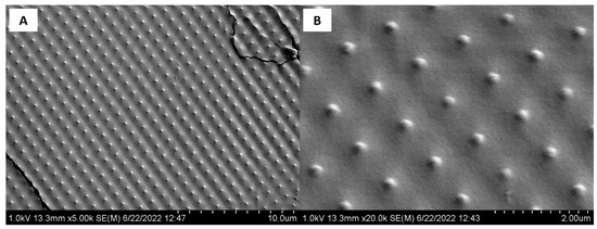
Figure 1.
Images captured using a scanning electron microscope showing the nanostructures at (A) 5000× and (B) 20,000× magnification.
3. Transmissivity Measurement
The samples were tested in a Perkins Elmer 950 UV-Vis spectrophotometer on a 400–860 nm wavelength range. This range was selected based on the maximum wavelength bandgap of the lamp available in the spectrometer at the time of testing. However, previously simulated work has shown that these nanostructures have the ability to be effective over a larger bandgap and that the periodicity influences the specific ranges where ALT is most prevalent [22]. These tests were conducted before the SEM images were taken, as the gold layer would alter the results. The lamp used for this range was a deuterium lamp which produces unpolarized radiation in the UV and visible light regions [29]. All tests were done at normal incidence. Tests ran at increments of 1 nm at a rate of 240 nm per minute. The rectangular sample
The size was smaller than the size of the light beam, so modifications were needed for the sample holding aperture. This modification was created using magnetic tape with a 2 mm hole that was adhered to the front surface of the sample holder to ensure the beam size was less than the patterned rectangle.
The spectrometer was first calibrated with the magnetic tape in place. The measured transmissivity was almost 100% with a small variation around this value, all being within the 3% accuracy expected from this tool. Thus, blocking a portion of the light beam was not found to impair tool operation. Next, the plain interface of the PDMS sample was tested as a control sample, for comparison with ALT interfaces. For this, the same PDMS sample containing the patterns was tested in the forward and backward directions in a location where the nanopattern was not present. This was done to isolate transmission differences caused by imperfections in the matrix material. For the non-patterned sections of the PDMS sample, the forward and backward directions should be identical. The “forward direction” is designated as a light incident on the side of the PDMS sample where the nanostructures are present, then through the rest of the matrix material as shown in the schematic illustrated in Figure 2. The “backward direction” is designated as the light incident on the side of the PDMS sample where no nanostructures are present. The light then propagates through the matrix material before reaching the surface where nanostructures are present. An average difference of 3% was found between forward and backward directions across the full range of wavelengths tested, which matches the experimental error for this tool.
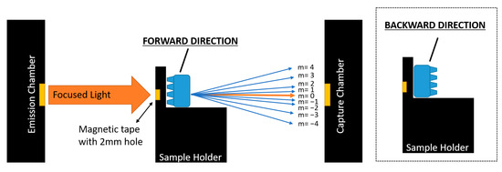
Figure 2.
Schematic showing the testing setup in the forward direction with the 2 mm magnetic tape focusing hole. The angular dispersion of the ALT grating with the sample oriented for “forward” direction data collection is illustrated. The sample mounting for testing in the backward direction is also shown.
Finally, to better understand the results presented in the next section, it is important to discuss the general operation of spectrophotometers. In an effort to reduce errors from scattered or diffused light, spectrophotometers typically strive to collect only light that passes straight through a sample [30]. In other words, spectrometers will collect primarily the 0th-order diffraction, ignoring scattering effects. An exaggerated schematic of this concept is shown in Figure 2. This becomes a problem when trying to test for asymmetric light transmission because, as previously explained, this effect works by blocking higher orders in one direction but allowing their propagation in the other direction. In both cases, 0th diffraction order light is able to propagate through, thus a transmission difference might be difficult to observe with a spectrophotometer. To understand if higher diffractions orders are captured by the detector, one can use the chamber spectrophotometer geometry and prediction of transmission grating equation,
where nm is the index of refraction of the grating, θm is the diffracted angle of propagation, ni is the index of refraction of the initial media (air), θi is the incident angle on the grating, m is the diffraction order, λ is the wavelength, and Λ is the grating period. Based on this equation, the angles for “lower” diffraction orders (m = −2, −1, 1, 2) of a PDMS grating with the same spacing as the pyramidal nanostructures investigated here fall anywhere from ±20° to ±65°. Using these angles and the distance between the sample and the collection slit, light in these diffraction orders would propagate outside the window for light collection even when considering the larger collection area as compared with the beam size (Figure 2). However, this is not necessarily true because the transmission grating equation may not be applicable to the interface investigated here as discussed next.
It has been demonstrated in recent work that Wood-Rayleigh anomalies can have up to a 5% angle variance in the metallic gratings [31]. More recent work on Wood’s anomalies suggests that resonance anomalies may occur in non-metallic corrugated periodic gratings [32]. They arise when the space between nanostructures acts as resonance cavities, producing a propagation pattern different from that from a standard diffraction grating, especially in the angular dispersion [32,33]. Similar effects have been observed in metamaterials based on amorphous silicon nanostructures engineered to manipulate second harmonic light and control its diffraction patterns [34]. All this evidence and along with the numerical modeling presented later, indicate that some of the lower (but not all) diffraction orders have been collected by the spectrometer detector.
For testing the patterned portions of the sample, the PDMS sample was placed in the holding aperture and the 2 mm hole was carefully aligned with the nanostructure array. Each patterned rectangle was subsequently tested for the forward and backward direction.
4. Comparison of Experimental and Numerical Data
The experimental results of the forward and backward transmission of ALT interfaces with 800 nm, 900 nm, and 1000 nm periodicity are shown in Figure 3A–C, respectively as a function of wavelength. The “reduced transmissivity” label of y-axis in Figure 3 is used to indicate the fact that only part of the transmitted light is collected, the lower diffraction orders. The results show that the 800 nm periodicity array performs the best, with an average 21% transmission difference across the entire wavelength interval between forward and backward transmission. The 900 nm periodicity also exhibited a 10% transmission difference. Finally, the 1000 nm periodicity showed virtually zero transmission difference. This is attributed to the fact that the spacing between nanostructures had become too large and these effects can no longer be found over the wavelength interval. The 800 nm and 900 nm transmissivity difference results are well above the experimental error of 3% attributed to the measurement tool. These results also occur over a 460 nm bandgap, which shows the broadband effect this pattern can hold. Additionally, despite the structures departing from the initial design specifications, the ALT effect is still present which speaks to this resilience to defects and variation.
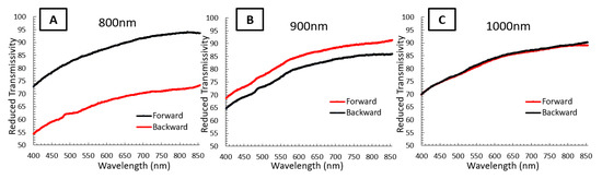
Figure 3.
Spectrophotometer measurements for forward and backward spectral transmissivity for (A) 800 nm, (B) 900 nm, and (C) 1000 nm periodicity sample. Experimental error is ±3%.
A pattern that does not need to strictly adhere to precise geometry will make mass manufacturing of similar designs a simpler process, especially as applied to LSCs.
In order to understand these experimental results, COMSOL simulations were created for comparison. The COMSOL model was set up using the same pyramidal structure as previous simulations [22] which inspired this experimental study except that the material for both the substrate and the nanostructure was changed to PDMS for a direct comparison. The previously simulated pyramidal shape was also modified slightly to match the shape of the structures expected from silicon molding. Specifically, the base, b, of the pyramid was set to 550 nm (as defined by EBEAM lithography), its height, h, was set to 550 nm, the estimated etch depth, and the pyramid sidewall was set to have 57.4° angle defined by KOH etch, seen in Figure 4A. A single unit cell for an 800 nm, 900 nm, and 1000 nm periodicity was modeled using periodic boundary conditions and the procedure described in detail in [22]. The simulation was run for both s- and p-polarizations. The results were averaged to obtain data for unpolarized light.
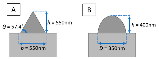
Figure 4.
(A) Schematic of the modified pyramid shape expected from the KOH etch with a base width, b = 550 nm, a height, h = 550 nm, and an etch angle, θ = 57.4°. (B) Schematic of the hemispherical ellipsoid with a periodicity of 800 nm used to simulate the estimated shape of the fabricated nanostructures where diameter, d = 350 nm, and height, h = 400 nm.
Figure 5 shows the predicted transmissivity as a function wavelength plotted along the experimental data for forward and backward directions. Two sets of predicted transmissivities are shown: total transmissivity including all diffraction orders and reduced transmissivity considering lower diffraction orders, m = (−2, −1, 0, 1, 2).
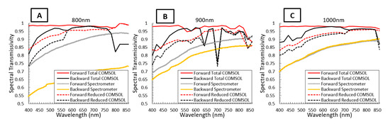
Figure 5.
Predicted total and reduced (m = (−2, −1, 0, 1, 2)) transmissivity in the forward and backward direction for (A) 800 nm, (B) 900 nm, and (C) 1000 nm periodicity. Experimental data are added for comparison.
When considering all diffraction orders for both directions, there is a predicted transmissivity difference of 5%, 4.5%, and 3% for periodicities of 800 nm, 900 nm, and 1000 nm, respectively. As with the experimental datasets in this study, the forward and backward transmissivity, the difference decreases as the periodicity increases. However, comparing the experimental results with predictions for total transmissivity, it becomes clear that trends differ.
Specifically, the experimentally measured forward transmissivity drops at a lower wavelength, while prediction accounting for all diffraction orders shows almost flat forward transmissivity over the wavelength interval.
On the other hand, when considering only the low diffraction orders, more specifically m = (−2, −1, 0, 1, 2) in forward and backward transmission, the spectral transmissivity follows the same downward trend seen experimentally with decreasing wavelength. This clearly indicates that the spectrophotometer collects lower diffraction orders as discussed previously. The transmission difference also decreases as the periodicity increases for both data sets. The predicted average transmissivity difference, in this case, is 4%, 2.5%, and 1.5% for 800 nm, 900 nm, and 1000 nm, respectively. A major difference still occurs in the 900 nm periodicity simulation results where several local minima occur. These low peaks are most likely “sharp” anomalies where the resulting periodicity of the manufactured nanostructures obscure large amounts of propagating light, as described by Woods [1]. In addition, predictions at 1000 nm periodicity still indicate a difference between forward and backward low-order transmission, while experimental data for the two directions overlap. Overall, although the prediction and experimental data agree in the fact that less difference is seen with increasing periodicity and that transmissivity drops at a lower wavelength, the transmission difference seen in experiments remains significantly larger than a prediction, which was somewhat surprising. Thus, the effect of the nanostructure shape on transmissivity was explored next.
The numerical results presented so far were based on a pyramid with a square cross-section and larger than what has been observed on SEM images of the fabricated samples. Additional simulations were run with an estimate of the actual shape of the fabricated nanostructures based on SEM micrograph measurements.
The new geometry considered in the COMSOL simulation was that of a hemispherical ellipsoid of 350 nm diameter and 400 nm height, as shown in Figure 4B. The COMSOL simulations were otherwise identical. Data were again collected for each periodicity for both the forward and backward direction. The results for unpolarized light were calculated by averaging the data for polarized light as done previously. The results of the forward and backward transmissivity for m = (−2, 1, 0, −1, −2) are shown in Figure 6 along with experimental data. The average spectral transmissivity differences calculated are 14.5%, 7.6%, and 5.5% for the 800 nm, 900 nm, and 1000 nm periodicities, respectively. This is more than double the transmissivity difference predicted for the pointed pyramid structure for the same included diffraction orders and closer to the experimentally seen differences. The numerical study continued to show the trend of a decreasing transmissivity difference as periodicity increases and all three plots follow downward curves with decreasing wavelengths seen in the pointed pyramid simulations discussed earlier. Still, the experimental data present a larger transmissivity difference. There could be several reasons for this discrepancy. It is important to remember that the geometry of this simulation is a rough estimate based on the SEM so differences in dimensions are to be expected. Additionally, there are variations in the nanostructures as a consequence of the fabrication process (namely the adherence of the PDMS to the silicon mold during removal). Despite these differences, the simulation results presented for the hemi-ellipsoid show a prediction closer to the experimental data than the pyramid structures which indicates that the geometry of the structure is playing a dominant role in the results.
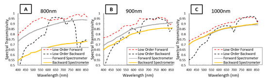
Figure 6.
Prediction for transmissivity of low diffraction orders (m = (−2, −1, 0, 1, 2)) in the forward direction and backward direction plotted against the data collected by the spectrophotometer for periodicities: (A) 800 nm, (B) 900 nm, and (C) 1000 nm.
The differences between numerical and experimental results presented here are similar to other ALT studies mentioned in the introduction. Giden et al. [5] had numerical results that showed more defined sharp peaks at several frequencies when compared to the experimental data, similarly to the discrepancies found in this work. Another example is the study conducted by Wang et al. [8] who compared numerical simulation data to experimental results. They also found that the two curves followed similar, but not identical, trends with the simulation data having more extreme variations. Additionally, the experimental transmissivity difference was about half that of the simulation data. In Shen et al. [7] their experimental data trends were similar to those predicted numerically, but only saw a 5–10% decrease in “transmission enhancement” compared to the 80% reported for numerical predictions. Finally, in Zhang et al. [9], while the average transmission difference in both the numerical and experimental results gave nearly identical results, the simulated values still showed more variation, while the experimental data displayed a more linear trend. Thus, it appears to be common that numerical data provide a larger transmission difference and predict a more extreme variation with larger peaks when compared with experimental data.
While previous studies were successful in creating an ALT interface, they use materials deposited on a different material substrate, such as gold or other dielectrics, and demonstrate an effect on a relatively narrow wavelength interval. The results presented in this paper show broadband effects and do so with the nanostructures and the substrate being a single piece and made from the same material, which has practical advantages.
5. Conclusions
In the recent past, researchers have been able to successfully create interfaces that show asymmetric light transmission effects mostly for applications in optical communication circuitry. In parallel, luminescent solar concentrators have gained interest as a potential technology for building integrated renewable energy systems. Their practical implementation depends, however, on improving their current optical efficiency. One way to improve the optical efficiency of LSCs is by preventing the light from escaping the LSC matrix via an ALT interface. However, creating an ALT interface usually requires expensive nanofabrication techniques to deposit and nanopattern a material onto the substrate. This paper presents proof-of-concept results showing, for the first time, that it is possible to create ALT interfaces using a single material acting as both the nanostructures and the substrate. The material used in this study is commonly employed as an LSC matrix. The procedure to create these interfaces is simple and cost-effective, based on wet-etched silicon wafers molds. The experimental results show a bandgap favorable to silicon solar cells. Specifically, the prototyped interfaces boast a 21% transmission difference for the 800 nm periodicity and a 10% transmission difference for the 900 nm periodicity, both with a 3% range of error. Results from numerical simulations carried out in COMSOL agreed well with the trends seen in the experimental data. The proof-of-concept results presented in this paper open the door for further work that can be done to optimize this manufacturing process and improve design effectiveness, which may potentially lead to ALT interfaces able to significantly increase LSC efficiency by increasing its light-trapping capabilities.
Author Contributions
Conceptualization, D.-A.B.-T. and V.O.; methodology, D.-A.B.-T., V.O. and M.H.; Software, V.O.; validation, V.O.; formal analysis, V.O.; investigation, V.O.; data curation, V.O., D.-A.B.-T. and M.H.; writing—original draft preparation V.O. and D.-A.B.-T.; writing—review and editing M.H. and D.E.S.; visualization, V.O.; supervision, D.-A.B.-T., M.H. and D.E.S.; project administration, D.-A.B.-T.; funding acquisition, D.E.S. All authors have read and agreed to the published version of the manuscript.
Funding
V.O. acknowledges the DoD SMART scholarship and Brookhaven National Laboratory, and Distributed Solar Development (DSD) for funding the experimental work. The DoD and DSD had no role in the study design, data collection, and analysis, decision to publish, or preparation of this manuscript.
Data Availability Statement
The data that support the findings of this study are available from the corresponding author upon request.
Conflicts of Interest
The authors declare no conflict of interest. The funders had no role in the design of the study; in the collection, analyses, or interpretation of data; in the writing of the manuscript, or in the decision to publish the results.
References
- Wood, R.W. On a Remarkable Case of Uneven Distribution of Light in a Diffraction Grating Spectrum. Proc. Phys. Soc. Lond. 1902, 18, 269–275. [Google Scholar] [CrossRef]
- Rayleigh, L. On the dynamical theory of gratings. Proc. R. Soc. Lond. Ser. A Contain. Pap. Math. Phys. Character 1907, 79, 399–416. [Google Scholar]
- Zhu, H.; Li, F.; Tang, B.; Zang, X.; Jiang, C. Asymmetric transmission through metallic grating with dielectric substrate. Opt. Commun. 2014, 318, 41–46. [Google Scholar] [CrossRef]
- Rahal, H.; AbdelMalek, F. Asymmetric transport of light in arrow-shape photonic crystal waveguides. Superlattices Microstruct. 2017, 103, 358–364. [Google Scholar] [CrossRef]
- Giden, I.H.; Yilmaz, D.; Turduev, M.; Kurt, H.; Çolak, E.; Ozbay, E. Theoretical and experimental investigations of asymmetric light transport in graded index photonic crystal waveguides. Appl. Phys. Lett. 2014, 104, 031116. [Google Scholar] [CrossRef]
- Bor, E.; Turduev, M.; Yasa, U.G.; Kurt, H.; Staliunas, K. Asymmetric light transmission effect based on an evolutionary optimized semi-Dirac cone dispersion photonic structure. Phys. Rev. B 2018, 98, 245112. [Google Scholar] [CrossRef]
- Shen, B.; Polson, R.; Menon, R. Broadband asymmetric light transmission via all-dielectric digital metasurfaces. Opt. Express 2015, 23, 20961–20970. [Google Scholar] [CrossRef]
- Wang, Y.-H.; Kim, I.; Jin, R.-C.; Jeong, H.; Li, J.-Q.; Dong, Z.-G.; Rho, J. Experimental verification of asymmetric transmission in continuous omega-shaped metamaterials. RSC Adv. 2018, 8, 38556–38561. [Google Scholar] [CrossRef]
- Zhang, C.; Pfeiffer, C.; Jang, T.; Ray, V.; Junda, M.; Uprety, P.; Podraza, N.; Grbic, A.; Guo, L.J. Breaking Malus’ law: Highly efficient, broadband, and angular robust asymmetric light transmitting metasurface. Laser Photonics Rev. 2016, 10, 791–798. [Google Scholar] [CrossRef]
- Hughes, M.D.; Smith, D.E.; Borca-Tasciuc, D.-A. Performance of wedge-shaped luminescent solar concentrators employing phosphor films and annual energy estimation case studies. Renew. Energy 2020, 160, 513–525. [Google Scholar] [CrossRef]
- Smith, D.E.; Hughes, M.D.; Borca-Tasciuc, D.-A. Towards a standard approach for annual energy production of concentrator-based building-integrated photovoltaics. Renew. Energy 2022, 186, 469–485. [Google Scholar] [CrossRef]
- Hughes, M.D.; Borca-Tasciuc, D.-A.; Kaminski, D.A. Highly efficient luminescent solar concentrators employing commercially available luminescent phosphors. Sol. Energy Mater. Sol. Cells 2017, 171, 293–301. [Google Scholar] [CrossRef]
- Debije, M.G.; Verbunt, P.P.C.; Rowan, B.C.; Richards, B.S.; Hoeks, T.L. Measured surface loss from luminescent solar concentrator waveguides. Appl. Opt. 2008, 47, 6763. [Google Scholar] [CrossRef] [PubMed]
- Slooff, L.; Burgers, A.; Debije, M. Reduction of escape cone losses in luminescent solar concentrators with cholosteric mirrors. Proc. SPIE 2008, 7043, 704306. [Google Scholar] [CrossRef]
- Connell, R.; Pinnell, C.; Ferry, V.E. Designing spectrally-selective mirrors for use in luminescent solar concentrators. J. Opt. 2018, 20, 024009. [Google Scholar] [CrossRef]
- Peters, I.M.; Goldschmidt, J.C.; Löper, P.; Prönneke, L.; Bläsi, B.; Gombert, A. Design of photonic structures for the enhancement of the light guiding efficiency of fluorescent concentrators. Photonics Sol. Energy Syst. II 2008, 7002, 70020V. [Google Scholar] [CrossRef]
- Connell, R.; Ferry, V.E. Integrating Photonics with Luminescent Solar Concentrators: Optical Transport in the Presence of Photonic Mirrors. J. Phys. Chem. C 2016, 120, 20991–20997. [Google Scholar] [CrossRef]
- Wang, J.; Yuan, Y.; Zhu, H.; Cai, T.; Fang, Y.; Chen, O. Three-dimensional macroporous photonic crystal enhanced photon collection for quantum dot-based luminescent solar concentrator. Nano Energy 2020, 67, 104217. [Google Scholar] [CrossRef]
- Debije, M.G.; Van, M.P.; Verbunt, P.P.; Kastelijn, M.J.; van der Blom, R.H.; Broer, D.J.; Bastiaansen, C.W. Effect on the output of a luminescent solar concentrator on application of organic wavelength-selective mirrors. Appl. Opt. 2010, 49, 745–751. [Google Scholar] [CrossRef]
- Verbunt, P.P.; Tsoi, S.; Debije, M.G.; Boer, D.J.; Bastiaansen, C.W.; Lin, C.W.; de Boer, D.K. Increased efficiency of luminescent solar concentrators after application of organic wavelength selective mirrors. Opt. Express 2012, 20 (Suppl. S5), A655–A668. [Google Scholar] [CrossRef]
- Verbunt, P.P.C.; Debije, M.G.; Broer, D.J.; Bastiaansen, C.W.M.; de Boer, D.K.G. Organic wavelength selective mirrors for luminescent solar concentrators. Photonics Sol. Energy Syst. IV 2012, 8438, 843805. [Google Scholar] [CrossRef]
- Oliveto, V.; Borca-Tasciuc, D.-A. Broadband asymmetric light transmission interfaces for luminescent solar concentrators. Nanoscale Adv. 2021, 3, 3627–3633. [Google Scholar] [CrossRef] [PubMed]
- Cargou, S. PDMS Membrane: Thickness of a Spin Coated PDMS Layer. Elveflow: Paris, France, December 2020. Available online: https://www.elveflow.com/microfluidic-reviews/soft-lithography-microfabrication/pdms-membrane-thickness-of-a-spin-coated-pdms-layer/ (accessed on 9 March 2022).
- Kim, J.-M.; Im, C.; Lee, W.R. Plateau-Shaped Flexible Polymer Microelectrode Array for Neural Recording. Polymers 2017, 9, 690. [Google Scholar] [CrossRef]
- Beadie, G.; Brindza, M.; Flynn, R.A.; Rosenberg, A.; Shirk, J. Refractive index measurements of poly(methyl methacrylate) (PMMA) from 0.4–1.6 μm. Appl. Opt. 2015, 54, F139–F143. [Google Scholar] [CrossRef]
- KOH Etch Calculator. Available online: http://xcapaldi.com/koh-calculator.html (accessed on 10 June 2022).
- KOH Etching|BYU Cleanroom. Available online: https://www.cleanroom.byu.edu/KOH (accessed on 10 June 2022).
- Wet Chemical Etching of Silicon and SiO2. p. 7. Available online: https://www.microchemicals.com/technical_information/silicon_etching.pdf (accessed on 10 June 2022).
- UV-Vis Spectroscopy Lambda 950 Hardware Guide. Available online: https://cmdis.rpi.edu/sites/default/files/UVVis-PerkinElmer-Lambda950-HardwareGuide.pdf (accessed on 20 June 2022).
- Reule, A.G. Errors in Spectrophotometry and Calibration Procedures to Avoid Them. J. Res. Natl. Bur. Stand. Sect. A Phys. Chem. 1976, 80, 609–624. [Google Scholar] [CrossRef] [PubMed]
- Tran, N.M.; Chioar, I.A.; Stein, A.; Alekhin, A.; Juvé, V.; Vaudel, G.; Razdolski, I.; Kapaklis, V.; Temnov, V. Observation of the nonlinear Wood’s anomaly on periodic arrays of nickel nanodimers. Phys. Rev. B 2018, 98, 245425. [Google Scholar] [CrossRef]
- Hessel, A.; Oliner, A.A. A New Theory of Wood’s Anomalies on Optical Gratings. Appl. Opt. 1965, 4, 1275–1297. [Google Scholar] [CrossRef]
- Ding, Y.; Magnusson, R. Band gaps and leaky-wave effects in resonant photonic-crystal waveguides. Opt. Express 2007, 15, 680–694. [Google Scholar] [CrossRef]
- Bar-David, J.; Levy, U. Nonlinear Diffraction in Asymmetric Dielectric Metasurfaces. Nano Lett. 2019, 19, 1044–1051. [Google Scholar] [CrossRef]


Publisher’s Note: MDPI stays neutral with regard to jurisdictional claims in published maps and institutional affiliations. |
© 2022 by the authors. Licensee MDPI, Basel, Switzerland. This article is an open access article distributed under the terms and conditions of the Creative Commons Attribution (CC BY) license (https://creativecommons.org/licenses/by/4.0/).