Article

Performance Enhancement of Interdigitated Heterojunction Solar Cells with Discotic Molecule

1
School of Electronics and Information, University of Electronic Science and Technology of China, Zhongshan Institute, Zhongshan 528402, China
2
South China Academy of Advanced Optoelectronics, South China Normal University, Guangzhou 510006, China
3
Beijing Dalu Instrument Technology Limited Company, Beijing 101199, China
*
Author to whom correspondence should be addressed.
Energies 2022, 15(15), 5736; https://doi.org/10.3390/en15155736
Submission received: 28 June 2022 / Revised: 22 July 2022 / Accepted: 4 August 2022 / Published: 7 August 2022

Abstract

:
Ordered interdigitated heterojunction as a promising nanostructure has attracted considerable attention due to its potential application in solar cells. However, a suitable construction to achieve effective free carrier transport in these nanostructures remains a challenge. In this study, interdigitated nanostructure was fabricated by combining vertically orientated TiO2 nanotube array with discotic liquid crystal Copper (II) 2,9,16,23-tetra-tert-butyl-29H,31H-phthalocyanine (tbCuPc). These discotic molecules were assembled as homeotropic alignment in the interdigitated nanostructure, which enhanced the carrier mobility of active layer considerably. The performance of photovoltaic cells with this interdigitated heterojunction was improved. Molecule orientation leading to charge carrier mobility enhancement was found to play a key role in improving the power conversion efficiency of the devices substantially.

1. Introduction

The organic solar cells have attracted considerable attention due to their potential application in manufacturing of effective low-cost, portable, and flexible devices [1,2,3,4]. However, the performance of organic solar cells depends on strong light absorption, effective exciton generation, diffusion, dissociation at the interface of heterojunction, and free carrier diffusion [4,5].
Provided that there is light absorption, excitons are generated in the photoactive layer, which diffuse to the interface between the donor and acceptor materials, and then dissociate into free carriers. Free carriers are transported by corresponding materials and collected on metal electrodes to form external circuits. However, there are some constraints in the process of exciton diffusion, dissociation, and free carrier transport. For most organic semiconductors, the exciton diffusion length is usually in the range of tens of nanometers [6,7]. Only excitons that diffuse to the vicinity of the heterojunction interface can be effectively dissociated, thus the exciton dissociation efficiency is limited by this length. Moreover, the free carriers produced by exciton dissociation have many recombination losses due to the discontinuity of the transmission channel. Furthermore, the carrier mobility of organic semiconductor materials is relatively low, and promoting the transmission of free carriers is also a key point. In order to improve the dissociation of excitons and prevent the recombination of free carriers before transmission to the electrode, it is necessary to design the appropriate morphology of the interface between donor and acceptor materials [8,9].
Among the heterojunction types, the most promising nanostructure is ordered interdigitated heterojunction, which is composed of bicontinuous and vertical crossing structures between donor and acceptor materials. Due to the large interfacial area of heterojunction, most photogenerated excitons are within the exciton diffusion length, which can diffuse to the interface and effectively dissociate into electrons and holes. Since the domains of donor and acceptor materials are arranged perpendicular to the electrode surface, almost all charge carriers could move along the uninterrupted path of the donor or acceptor until they reach their respective electrodes, which could improve the charge carrier transport and minimize the charge recombination efficiency of organic molecules [10,11]. At present, interdigitated nanostructure has been realized by several fabrication technologies and processes, such as nano imprint lithography [10,12,13], electron beam lithography [14,15], soft-templating [16], and electrochemical process [17,18]. In the organic solar cells field, ordered titanium dioxide nanostructures have been used to prepare interdigitated heterojunction solar cells [19,20,21], where the TiO2 ordered nanostructures have been used for enhancing light absorption [22], charge separation [23,24], and charge transport capability [25]. Nevertheless, in order to further improve the performance of organic photovoltaic devices, it is necessary to improve charge carrier transport and reduce recombination [26,27].
Here, we report the use of TiO2 ordered vertically orientated nanotube array combined with discotic liquid crystal to fabricate interdigitated nanostructure. The discotic liquid crystal is one class of promising organic semiconductors. These molecules are usually stacked on top of each other in columns by self-assembling. Due to this self-organization, strong orbital overlap will occur in one dimension, resulting in the improvement of carrier mobility along the column direction [28,29]. Normally, there are two self-assembly methods for discotic molecules: Homogeneous alignment and homeotropic alignment. The former has the edge-on orientation of molecules and the molecular packing columns are parallel to the substrate; the latter has the face-on orientation and the molecular packing columns are perpendicular to the substrate. Different device configurations require different molecular arrangements between electrodes. The discotic molecule alignment should be homeotropic in solar cells [30,31], which could improve the charge carriers transport through the active layer and allow the charge carriers to move easily perpendicular to the substrate [32]. However, it is difficult to change the orientation of discotic molecule and fabricate uniform films, thus it is rarely used for the preparation of photovoltaic devices.
In this report, the TiO2 vertically orientated nanotube array has been used indirectly as templates for deposition of discotic liquid crystal, and the molecular alignment could be changed from homogeneous to homeotropic, which is conducive to the application of photovoltaic devices. Furthermore, interdigitated heterojunction and uniform composite films have been obtained for the solar cells’ preparation.

2. Materials and Methods

2.1. Materials

Glycerin, ammonium sulfate, and ammonium fluoride were purchased from Thermo Fisher. Copper (II) 2,9,16,23-tetra-tert-butyl-29H,31H-phthalocyanine (tbCuPc) was purchased from Sigma-Aldrich. All chemicals were used as ex-bottle without purifications.

2.2. Preparation of Titanium Dioxide Nanotubes

Titanium film was deposited on the fluorine doped tin oxide coated (FTO) glass by RF reactive magnetron sputtering, and then the titanium film was anodized to obtain titanium dioxide nanotubes array [33,34,35]. The electrochemical cell was set up with a two-electrode configuration using the Ti coated FTO glass as a working electrode and platinum foil as a counter electrode under magnetic stirring. The anodization was performed in present of an electrolyte solution at a constant potential and at room temperature in order to form nanotube arrays with a range of diameters. The electrolyte solution was a mixture composed of de-ionized water (10 vol%), glycerin (90 vol%), ammonium fluoride (0.5 wt%), and ammonium sulfate (1.5 wt%). Anodization reaction was carried out with a fixed potential in the range from 20 to 35 V for 25 min to form nanotubes of different diameters from 40 to 100 nm. The samples were rinsed repeatedly with de-ionized water in an ultrasonic bath to remove surface debris and clean the electrolyte. After annealing at 500 °C for 1 h, the TiO2 nanotube array layers were obtained.

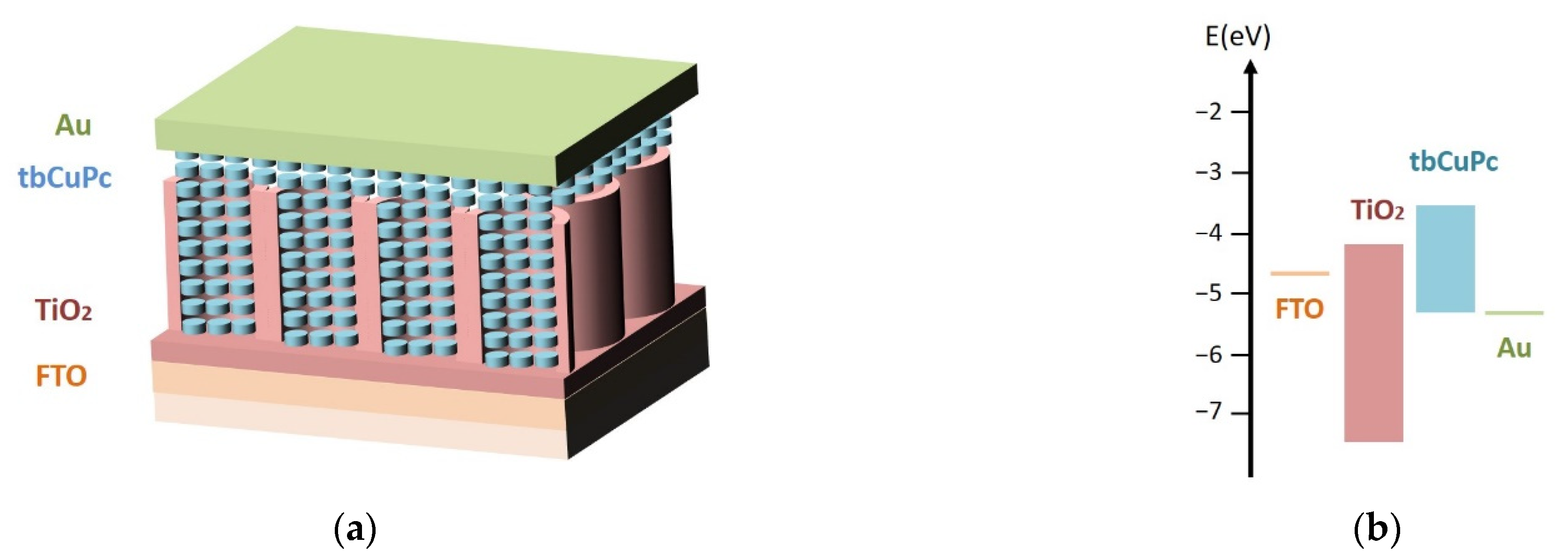
2.3. Device Fabrication

Interdigitated junction photovoltaic devices were prepared on top of TiO2 nanotube layers. The FTO substrates with TiO2 nanotubes were soaked in tbCuPc chlorobenzene solution for about 1 h and annealed for 30 min at 110 °C to remove the solvent. Thereafter, a thin film of gold was deposited on top of tbCuPc layers through a metal mask and laminated with glass to be sealed.
Planar junction photovoltaic devices were fabricated on top of FTO coated glass substrates with active layers made of TiO2 and tbCuPc films successively. Titanium films were deposited by radio-frequency reactive magnetron sputtering, and then annealed for 1 h at 500 °C to oxidize the titanium completely [34,36]. The tbCuPc films were deposited on top of the TiO2 layers by thermal evaporation. Finally, a top contact of gold was vacuum-evaporated through a metal mask and laminated with glass for sealing.

2.4. Test and Measurements

The morphology of the titanium nanotube film was examined by field emission scanning electron microscope (FE-SEM) (Hitachi 4800S). Polarized optical microscopic images were observed using an optical microscope (Leica DMRX). Current voltage measurements were performed using semiconductor characterization system (Keithley 4200-SCS). Photovoltaic responses were measured under a solar simulator (TriSol Solar Simulator TSS-156) at 100 mW/cm2. All measurements were carried out at room temperature in ambient condition.

3. Results and Discussion

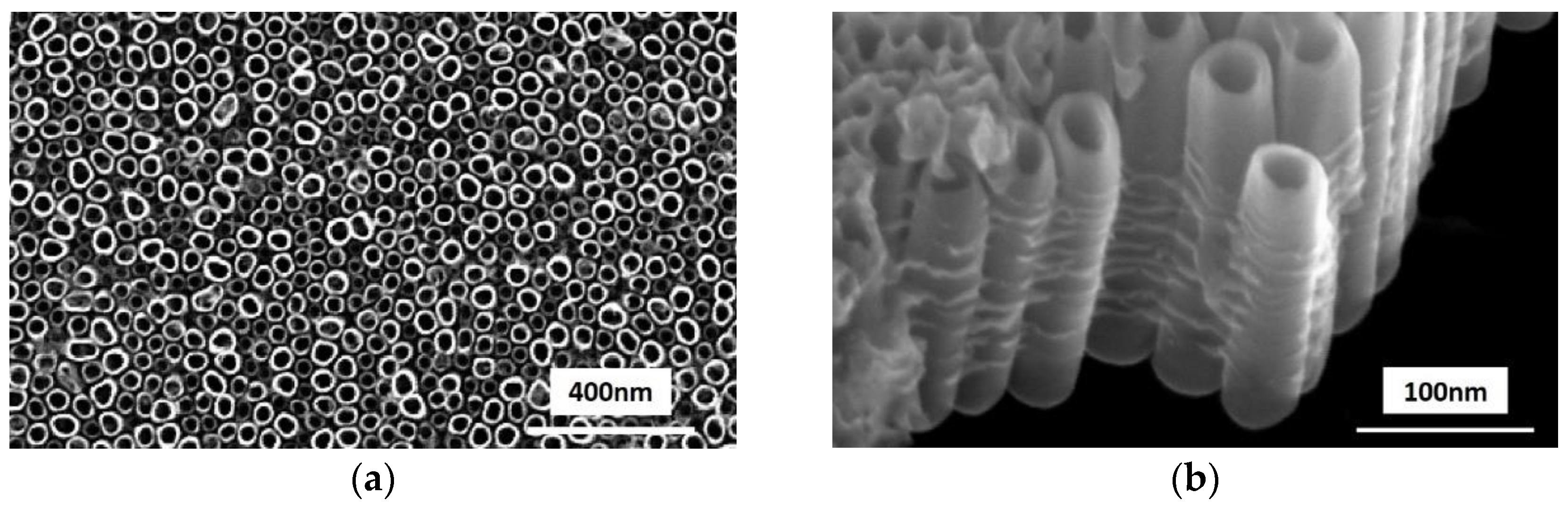
3.1. Morphology of Vertically Orientated TiO2 Nanotubes Array

The anodization reaction converted the top surface of Ti films into nanotubes array and covered the unreacted titanium metal film. Thereafter, the annealing process ensured that Ti films were oxidized completely. Surface morphology of the TiO2 films were further analyzed using scanning electron microscopy and the images are shown in Figure 1. It was found that TiO2 nanotube structures were highly orientated and arranged vertically in very tight bundles on the FTO glass. The top ends (Figure 1a) of nanotubes are opened, whereas the bottom ends of nanotubes are closed. The nanotube diameter could be estimated from the top-view image, and the side-view (Figure 1b) image reveals the length of nanotubes.
The diameter of nanotubes is highly dependent on the anodic oxidation potential [36]. When increasing the anodization potential, nanotube diameters can be increased as well to achieve a better size for the solar cells’ preparation. For example, if an anodization potential of 25 V was applied to react for 25 min, the nanotubes would be about ~60 nm in inner diameter, ~6 nm in wall thickness. If 35 V were applied, the nanotubes would be about ~100 nm in inner diameter, ~5 nm in wall thickness. The anodization potential and its corresponding nanotube diameter parameters are listed in Table 1.

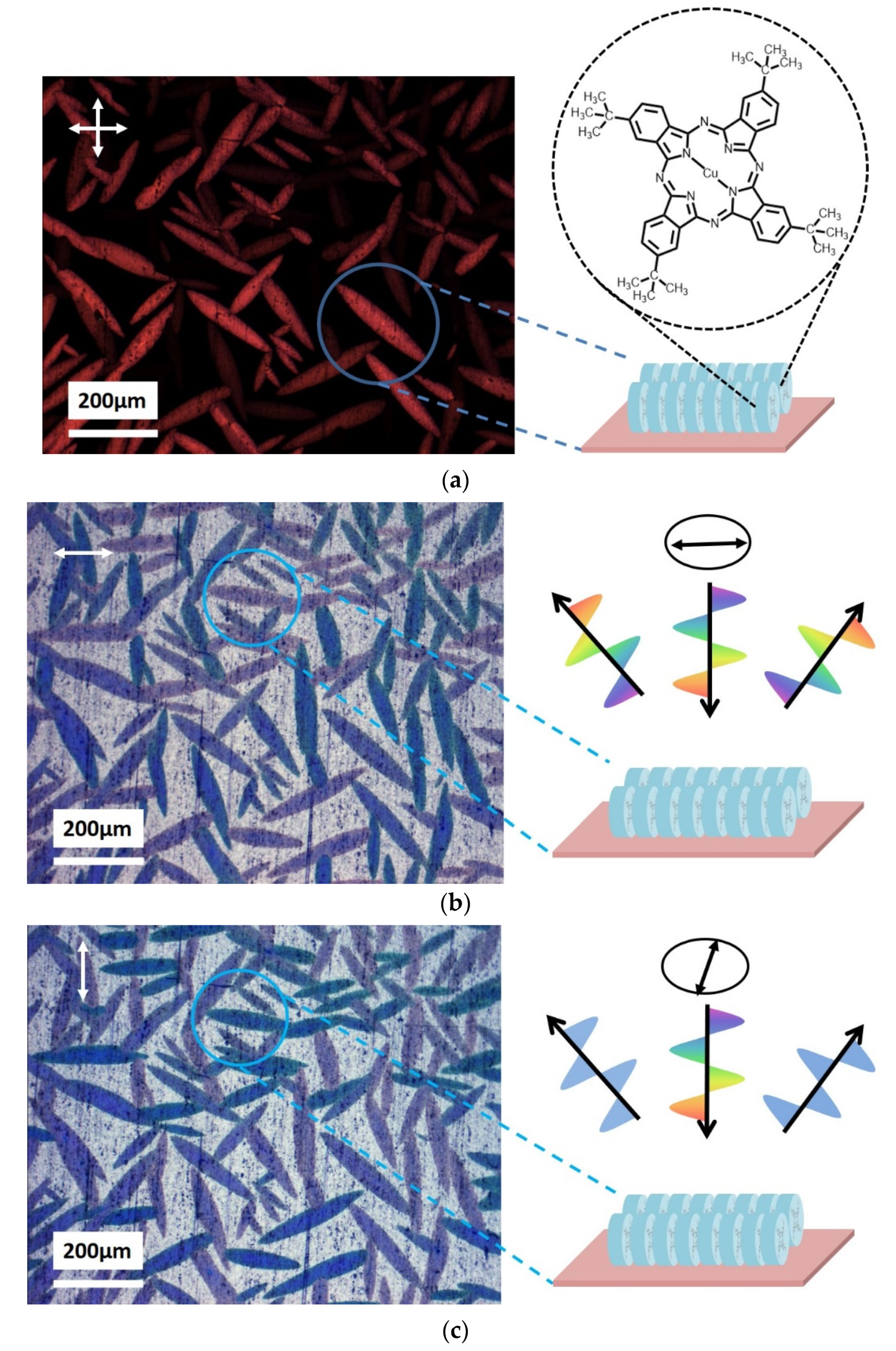
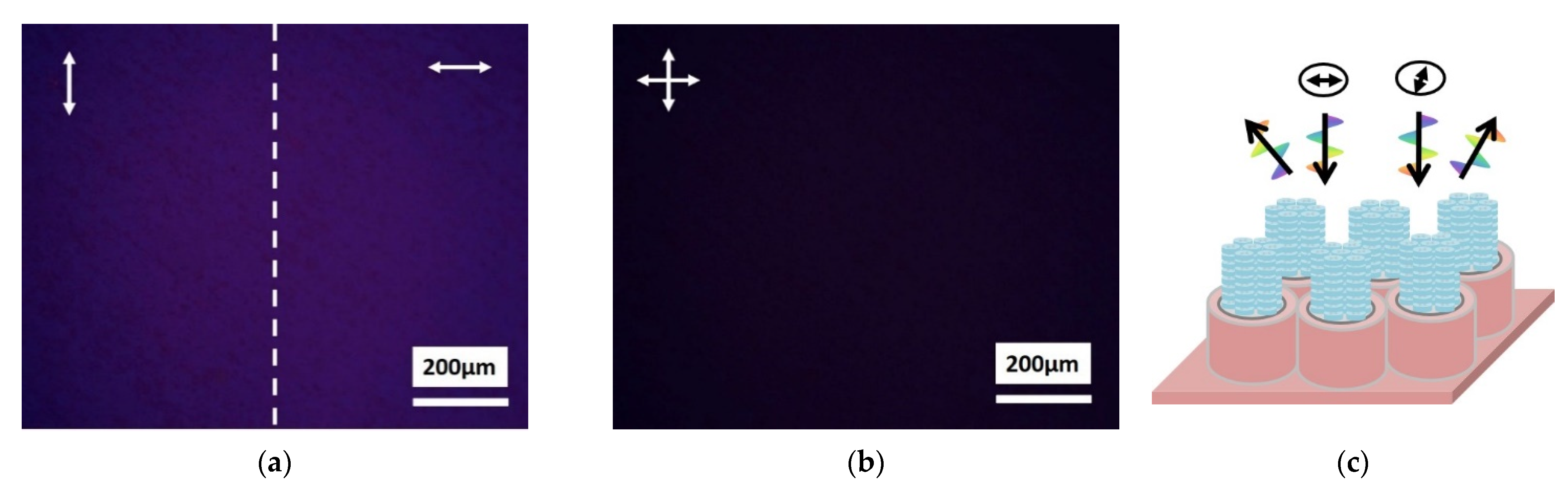
3.2. Molecules Alignment in Composite Film

Initially, the tbCuPc molecule alignment on smooth TiO2 film should be investigated. The specimen was prepared by dripping a drop of tbCuPc chloral benzene solvent on TiO2 film, and then the chloral benzene evaporated. The tbCuPc crystallized on the film surface and a needle-like texture could be observed (Figure 2). The polarization direction in Figure 2 is indicated by the double-headed arrow. Figure 2a is an optical micrograph of the tbCuPc crystal with cross-polarized condition. This is similar to the phenomenon of birefringence. The contrast results from rotation of polarized light through the crystal domain. Meanwhile, the crystal domains whose crystallographic axis is parallel to polarizer are extinguished, and the other oblique domains are still visible. The domains with an angle of 45° between crystal axis and polarizer are the clearest.
Figure 2b and c are optical micrographs of the tbCuPc discotic molecule illuminated with linear polarized light in the same position. Polarization direction of illuminating light is also shown by a double-headed arrow. The needle-like texture of the tbCuPc crystals change color from heavy blue to French grey, which could be observed if we rotated the polarizer in front of light source (Figure 2b,c). This difference in the grey shades of crystal domain depends on tbCuPc molecule orientation relative to the polarization axis.
Normally, intramolecular excitation and electron transition are considerably stronger than intermolecular transition [37,38,39,40], leading to the stronger intramolecular absorption, as well [38,41]. The most possible transition would occur if the electric field vector of the linear polarized light was parallel to the molecular plane, resulting in the strongest intramolecular absorption. Therefore, the stronger absorption shows the original color of tbCuPc, namely, heavy blue.
The color of crystal domains indicates molecule assembling on the TiO2 surface. When polarization direction is parallel to the optical axis (Figure 2b), the crystal domains appear French grey, which indicates that the linear light polarization direction is perpendicular to tbCuPc molecule plane and poor intermolecular absorption, thus the absorbance of crystal domain reaches the minimum. While a polarizer orientation rotated 90° (Figure 2c), crystal domains appear to be heavy blue due to the fact that the linear light polarization direction is parallel to tbCuPc molecule plane, and thus the absorbance of tbCuPc molecule reaches the maximum. This pleochroism arises as tbCuPc molecules are stacked face-to-face along the extinguished axis (edge-on orientation), which is parallel to the plane of TiO2 substrate as shown in Figure 2. This phenomenon indicates that tbCuPc molecules stacking axis prefers to be aligned parallel to the substrate surface (edge-on orientation or homogeneous alignment). It is similar to the report which states that tbCuPc molecules planes orientated perpendicular to silicon substrate [42].
Morphology of tbCuPc films changes significantly, after combining with vertically orientated TiO2 nanotubes. The preparation method was consistent with the smooth TiO2 film substrate. The molecule alignment of tbCuPc has also been investigated with polarization optical microscope. As shown in Figure 3a, a heavy blue uniform film can be seen, when the composite film is illuminated with linear polarized light. At this time, the incident light with perpendicular and parallel polarization directions are used respectively. Compared with Figure 2b,c, there is no change in color and no large crystal domain at the same magnification. The strongest intramolecular absorption is observed, making the composite film heavy blue as a whole. Therefore, the molecular planes of tbCuPc are parallel to the substrate (face-on orientation), when the polarization direction of the incident light is parallel to the substrate. Eventually, no birefringence could be observed through a microscope with two cross polarizers (Figure 3b). Compared with Figure 2a, there is no optically visible crystal domain, indicating that the molecular stacking axes are perpendicular to the substrate.
Considering the tbCuPc crystallization behavior on smooth TiO2 surface, this indicates that the molecular packing columns tend to be aligned with the substrate surface. Therefore, tbCuPc molecules tend to stack along the nanotubes wall after compounding with TiO2 nanotubes, assembling as homeotropic alignment (face-on orientation) as schematically represented in Figure 3c.
The optical microscope confirms that the tbCuPc molecular orientation has been changed during the nanotubes combining process, and it is particularly simple to achieve homeotropic alignment with vertically orientated nanotube array. This alignment of discotic molecule materials is instrumental in carrier transport, which is critically important for the application of discotic liquid crystal materials in optoelectronic devices. Moreover, it is shown that the composite film is very uniform and smooth, unlike other processes in which the film would break into islands and discontinued.

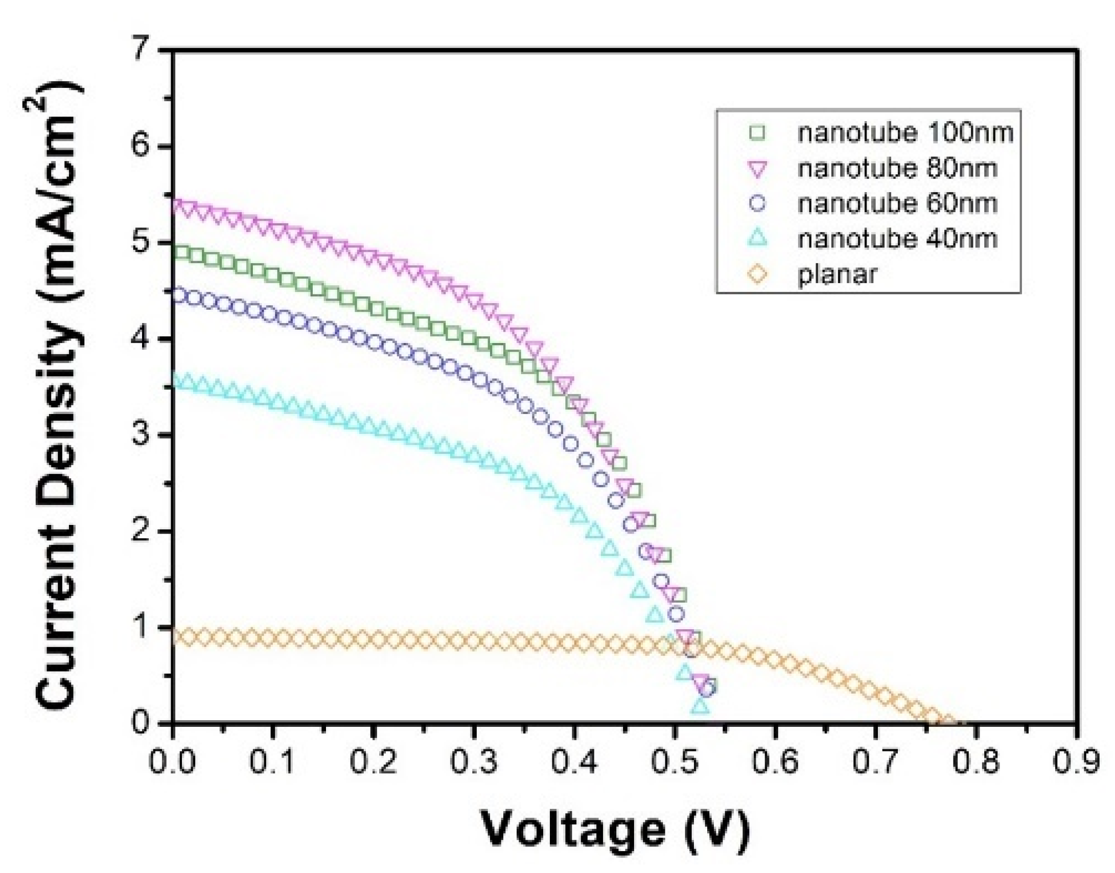
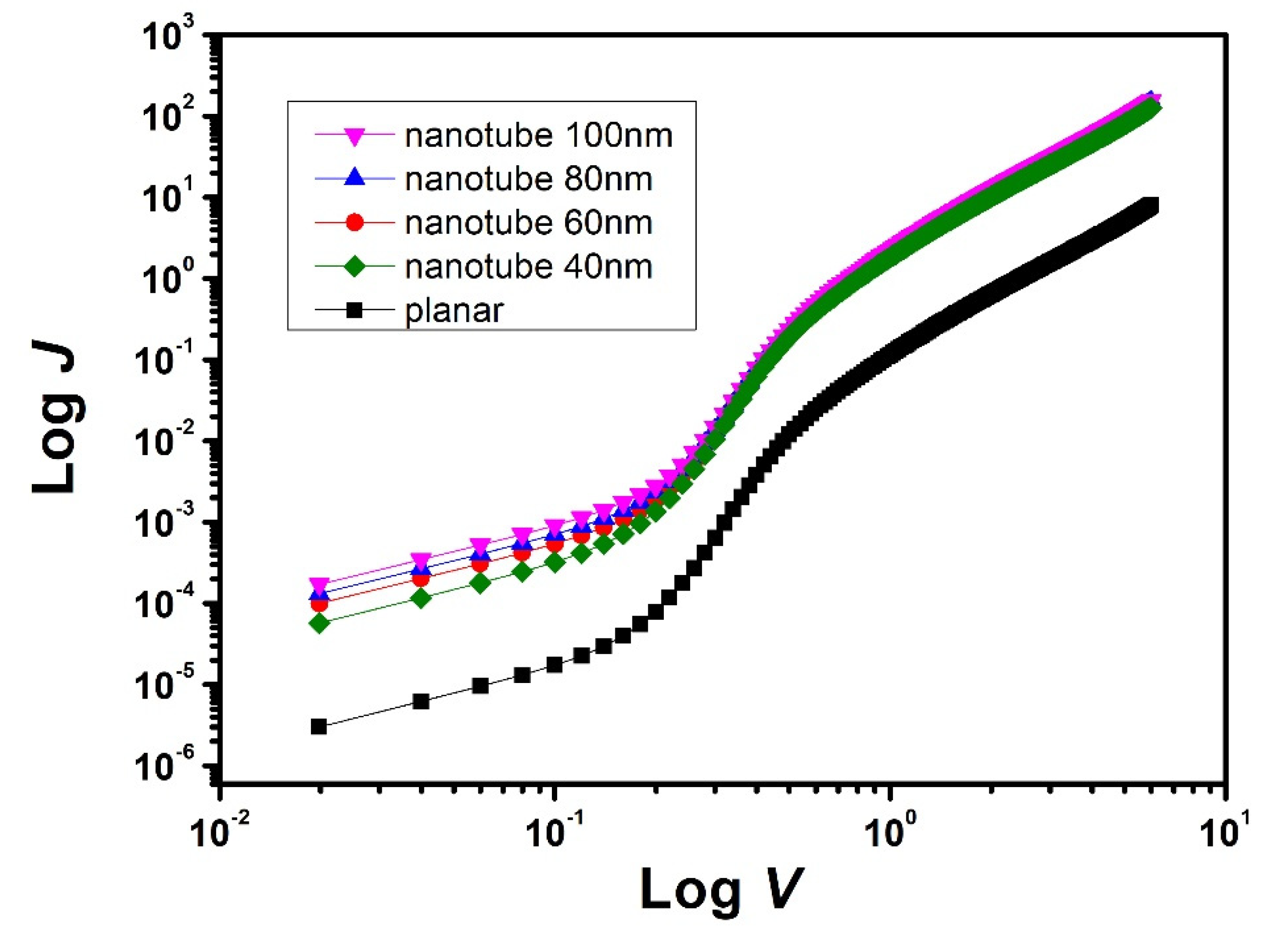
3.3. Performance of Solar Cells

Based on the homeotropic alignment of tbCuPc molecules combined with TiO2 nanotubes, a series of photovoltaic devices were fabricated with interdigitated heterojunction configuration comprising FTO/TiO2:tbCuPc/Au. A wide range of nanotubes were prepared, in which the diameters were varied in the range from 40 to 100 nm. Moreover, planar heterojunction device was prepared together as a comparison. The structure of interdigitated junction device is shown in Figure 4a. The transmission channel formed by the face-to-face stacking of tbCuPc was interspersed with TiO2 nanotubes to form interdigitated heterojunction. Electrons and holes could reach the electrode along two transmission channels, respectively. Energy level diagram of the solar cell was presented in Figure 4b. According to the band structure, tbCuPc was matched well with TiO2, which was conducive to the dissociation of photogenerated excitons and the transport of charge carriers.
The photovoltaic responses of planar heterojunction and interdigitated heterojunction devices were determined and the data were plotted in Figure 5. The average values of device parameters were listed in Table 2, and the detailed parameters of each device were shown in Table S1.
Data analysis reveals that the morphology of heterojunction interface between TiO2 and tbCuPc has a strong influence on the short circuit current (Jsc) of the devices. Compared with the planar heterojunction, the Jsc of the interdigitated heterojunction has a greater improvement, for instance, from 0.77 mA of the planar heterojunction device (device 5) to 3.56 mA of device 4 (40 nm nanotubes). The Jsc was gradually increased with the diameters of TiO2 nanotubes, i.e., from 3.56 mA/cm2 in device 4 to a maximum value of 5.42 mA/cm2 in device 2 (80 nm nanotubes). Then, it decreased as the diameters of TiO2 nanotubes were further increased, from 5.42 mA/cm2 (device 2) to 4.92 mA/cm2 in device 1 (100 nm nanotubes). This indicates that the Jsc of interdigitated heterojunction devices initially was increased and then decreased with the diameter of TiO2 nanotubes.
The trend in filling factor (FF) was different from Jsc. The maximum FF appeared in planar heterojunction device, which was 60%. However, the FF of the interdigitated heterojunction device was all less than 50%, and increased slightly with the nanotube diameter.
The magnitude of the series resistance and the shunt resistance could be approximated according to the intercept of the J-V characteristics near the open circuit voltage (Voc) and Jsc regions, respectively [43]. As can be seen from the J-V curve shown in Figure 5, the shunt resistance and the series resistance of interdigitated heterojunction devices are relatively smaller than those of planar devices. The increment of interfacial area and complexity of heterojunction seem to reduce the series resistance and shunt resistance at the same time. It is also shown that the reduction of shunt resistance has a greater impact on the photovoltaic responses, which eventually reduced the FF of interdigitated devices.
The open circuit voltage (Voc) of the planar heterojunction device was the maximum. It was lower in interdigitated heterojunction device, but slightly increased with diameters of TiO2 nanotubes from 0.52 to 0.55 V, when the diameters of nanotubes were increased from 40 to 100 nm. In fact, the overall power conversion efficiency of device 2 was among the best of these devices, exhibiting a 235% improvement to 1.41% from 0.42% in device 5.
In order to understand the reason for the increase in Jsc caused by the introduction of interdigitated junction, a series of electron-only devices with different nanotube diameters were prepared. The device structure was FTO/TiO2:tbCuPc/LiF/Al, which promoted electrons injection at the electrode and prevented holes. The space charge limited current (SCLC) method could be used to evaluate the charge carrier mobility in the active layer [44,45,46]. Dark J-V characteristics of the above devices were represented by the double logarithmic scale (Figure 6). It can be clearly seen that the current density of interdigitated devices has been increased in the whole voltage range compared with the current density of planar devices. According to the SCLC characteristics, the dark J-V characteristics met the power law relationship, namely, J ∝ Vm. As shown in Figure 6, there is a linear relationship between the current and voltage at a relatively low electric field, i.e., J ∝ V1, which indicates that single electron devices formed an ohmic contact. As the voltage increased, the current was raised to the trap filled limited region. The voltage was increased further and finally reached the saturated current region, where J ∝ V2. The electron mobility can be evaluated by the Child-Langmuir formula [28,44,45], as follows:
J = 9 8 ε ε 0 μ V 2 L 3
In the formula, μ is the electron mobility in these devices; ε is the relative dielectric constant; ε0 is the permittivity constant of free space; and L is the thickness of active layer. Electron mobility can be obtained from the interception of lnJ~lnV plot in Figure 6 [28]. The mobility of planar junction devices was 9.6 × 10⁻⁶ cm2/Vs, and the mobility of interdigitated junction devices was about 1.2 × 10⁻⁴ cm2/Vs. These results show that the electron mobility of interdigitated heterojunction was one order of magnitude higher than the planar heterojunction. The enhancement of charge carrier mobility may lead to the increase in Jsc, and the reason for this enhancement of mobility results from the change in tbCuPc orientation.
From the previous dark J-V characteristics, it has been proved that the significant enhancement of Jsc is closely related to the improvement of charge carrier transporting. At the same time, the increment of heterojunction interface caused by nanotubes led to the relatively high efficiency of exciton separation at the interface of TiO2/tbCuPc. Specifically, with the introduction of TiO2 nanotubes, the improvement of charge carrier mobility and exciton separation efficiency may help in raising the Jsc of the devices, to improve the photovoltaic performance. However, the increment of charge carrier mobility usually leads to the reduction of Voc [47,48], which caused the Voc of interdigitated heterojunction devices to be significantly lower than the planar heterojunction device (Table 2).
It must be noted that increasing the nanotube diameter would reduce exciton separation to reduce the Jsc of photovoltaic devices, which is detrimental to the performance of devices. Due to the change in nanotube diameter, the junction interface in this study also changed. The larger the TiO2 nanotube diameter, the smaller the interfacial area of interdigitated heterojunction. Both the exciton separation efficiency and the carrier recombination were reduced with the decrease in the interfacial area. The exciton separation promotes the Jsc of photovoltaic devices, but the carrier recombination reduces it [10]. However, the change trend was different with the decrease in junction interface. Therefore, it could be seen from the performance that the reduction of carrier recombination led to the increment of Jsc, when the nanotube diameter was increased from 40 to 80 nm. Then, the current of 80 nm device reached the maximum. As the nanotube diameter was increased to 100 nm, Jsc was also decreased due to the lower exciton separation.
For the 40 nm nanotube devices, carrier recombination in the active layer was very large compared with exciton separation. When the diameter of TiO2 nanotube was increased gradually from 40 to 80 nm, carrier recombination was reduced as junction interface, then the Jsc and FF were increased gradually. There seems to be a diameter threshold where the decrease in carrier recombination led to the maximum of carrier density. The recombination rate might be reduced to a level where carrier density could be substantially enhanced if the junction interface is reduced. This could contribute to the increment in the Jsc as the diameter of TiO2 nanotube was increased. As the nanotube diameter was further increased over 80 nm, the exciton separation reduction could be the reason accounting for the reduction of Jsc at a relatively lower interfacial area. In addition, carrier recombination is the main factor for Voc and FF reduction [26,27,49]. As shown in Table 2, the Voc of interdigitated junction devices was reduced by about half compared with the planar junction devices due to the adoption of nanotubes. However, the open circuit voltage was raised slightly with the increment of nanotube diameter.
The current result is interesting. Vertically oriented TiO2 nanotubes not only improved the charge carrier mobility of organic materials, but also promoted exciton dissociation at the interdigitated junction interface. Further adjusting the heterojunction interface of the active layer could optimize the balance between exciton dissociation and carrier recombination to improve the performance of photovoltaic devices.

4. Conclusions

Vertically orientated TiO2 nanotube array has been synthesized and combined with discotic liquid crystal tbCuPc to fabricate interdigitated heterojunction photovoltaic devices. In this study, it was revealed that the TiO2 nanotube array was helpful for the discotic molecule to assemble to an homeotropic alignment (face-on orientation), which could significantly enhance the carrier mobility in active layer. The increment of heterojunction interface and charge carrier transmission promoted the response of photovoltaic device. To further improve the performance of organic solar cells, it is necessary to balance the exciton dissociation and carrier recombination of interdigitated heterojunction interface.

Supplementary Materials

The following supporting information can be downloaded at: https://www.mdpi.com/article/10.3390/en15155736/s1. Table S1: Photovoltaic parameters of each device with different nanotube diameters.

Author Contributions

Methodology, Z.Z. (Zhi Zhang); validation, Z.Z. (Zhi Zhang); formal analysis, Z.Z. (Zhi Zhang), Y.W. and Q.C.; investigation, Z.Z. (Zhi Zhang), Y.W. and Q.C.; resources, Z.Z. (Zhipan Zeng); data curation, Y.W. and Q.C.; writing—original draft preparation, Y.W.; writing—review and editing, Z.Z. (Zhi Zhang); visualization, Z.Z. (Zhi Zhang); supervision, Z.Z. (Zhi Zhang); project administration, Z.Z. (Zhi Zhang); funding acquisition, Z.Z. (Zhi Zhang). All authors have read and agreed to the published version of the manuscript.

Funding

This research was funded by the High Level Talent Research Starting Project in University of Electronic Science and Technology of China Zhongshan Institute, grant number 417YKQ07, In-novation Team of Colleges and Universities in Guangdong Province, grant number 2020KCXTD030, the Characteristic Innovation Project in Universities and Colleges of Guangdong Provincial Department of Education, grant number 2018KTSCX290, and the Science and Technology Project Foundation of Zhongshan, grant number 2019B2027.

Institutional Review Board Statement

Not applicable.

Informed Consent Statement

Not applicable.

Data Availability Statement

Not applicable.

Conflicts of Interest

The authors declare no conflict of interest.

References

  1. Schopp, N.; Brus, V.V. A Review on the Materials Science and Device Physics of Semitransparent Organic Photovoltaics. Energies 2022, 15, 4639. [Google Scholar] [CrossRef]
  2. Riede, M.; Spoltore, D.; Leo, K. Organic solar cells—The path to commercial success. Adv. Energy Mater. 2021, 11, 2002653. [Google Scholar] [CrossRef]
  3. Fukuda, K.; Yu, K.; Someya, T. The future of flexible organic solar cells. Adv. Energy Mater. 2020, 10, 2000765. [Google Scholar] [CrossRef]
  4. Hu, Z.; Wang, J.; Ma, X.; Gao, J.; Xu, C.; Yang, K.; Wang, Z.; Zhang, J.; Zhang, F. A critical review on semitransparent organic solar cells. Nano Energy 2020, 78, 105376. [Google Scholar] [CrossRef]
  5. Anagnostou, K.; Stylianakis, M.M.; Petridis, K.; Kymakis, E. Building an Organic Solar Cell: Fundamental Procedures for Device Fabrication. Energies 2019, 12, 2188. [Google Scholar] [CrossRef] [Green Version]
  6. Sajjad, M.; Blaszczyk, O.; Jagadamma, L.; Roland, T.; Chowdhury, M.; Ruseckas, A.; Samuel, I.W. Engineered exciton diffusion length enhances device efficiency in small molecule photovoltaics. J. Mater. Chem. A 2018, 6, 6. [Google Scholar] [CrossRef] [Green Version]
  7. de Sousa, L.E.; Bueno, F.T.; Ribeiro, L.; Ribeiro Junior, L.A.; da Silva Filho, D.A.; de Oliveira Neto, P.H. Role of Exciton Density in Organic Materials: Diffusion Length, Lifetime, and Quantum Efficiency. Chem. Mater. 2019, 31, 6818–6823. [Google Scholar] [CrossRef]
  8. Kim, J.H.; Schaefer, C.; Ma, T.; Zhao, J.; Turner, J.; Ghasemi, M.; Constantinou, I.; So, F.; Yan, H.; Gadisa, A. The Critical Impact of Material and Process Compatibility on the Active Layer Morphology and Performance of Organic Ternary Solar Cells. Adv. Energy Mater. 2019, 9, 1802293. [Google Scholar] [CrossRef]
  9. Zhu, R.; Man, S.W.; You, L.; Santi, P.; Ratti, C. The effect of urban morphology on the solar capacity of three-dimensional cities. Renew. Energy 2020, 153, 1111–1126. [Google Scholar] [CrossRef]
  10. Xu, X.P.; Yu, L.Y.; Meng, H.F.; Dai, L.M.; Yan, H.; Li, R.P.; Peng, Q. Polymer Solar Cells with 18.74% Efficiency: From Bulk Heterojunction to Interdigitated Bulk Heterojunction. Adv. Funct. Mater. 2022, 32, 2108797. [Google Scholar] [CrossRef]
  11. Chevuntulak, C.; Rakpaises, T.; Sridumrongsak, N.; Thainoi, S.; Kiravittaya, S.; Nuntawong, N.; Sopitpan, S.; Yordsri, V.; Thanachayanont, C.; Kanjanachuchai, S. Molecular Beam Epitaxial Growth of Interdigitated Quantum Dots for Heterojunction Solar Cells. J. Cryst. Growth 2019, 512, 159–163. [Google Scholar] [CrossRef]
  12. Eisenhauer, D.; Trinh, C.; Amkreutz, D.; Becker, C. Light management in crystalline silicon thin-film solar cells with imprint-textured glass superstrate. Sol. Energy Mater. Sol. Cells 2019, 200, 109928. [Google Scholar] [CrossRef]
  13. Sun, P.; Li, X.; Shao, J.; Braun, P. High-Performance Packaged 3D Lithium-Ion Microbatteries Fabricated Using Imprint Lithography. Adv. Mater. 2021, 33, 2006229. [Google Scholar] [CrossRef]
  14. Mercier, T.M.; Rahman, T.; Krishnan, C.; Khorani, E.; Shaw, P.J.; Pollard, M.E.; Boden, S.A.; Lagoudakis, P.G.; Charlton, M.D. High symmetry nano-photonic quasi-crystals providing novel light management in silicon solar cells. Nano Energy 2021, 84, 105874. [Google Scholar] [CrossRef]
  15. Kim, M.S.; Lee, J.H.; Kwak, M.K. Surface texturing methods for solar cell efficiency enhancement. Int. J. Precis. Eng. Manuf. 2020, 21, 1389–1398. [Google Scholar] [CrossRef]
  16. Malgras, V.; Shirai, Y.; Takei, T.; Yamauchi, Y. Coalescence-Driven Verticality in Mesoporous TiO2 Thin Films with Long-Range Ordering. J. Am. Chem. Soc. 2020, 142, 15815–15822. [Google Scholar] [CrossRef] [PubMed]
  17. Wang, D.; Liu, L. Continuous fabrication of free-standing TiO2 nanotube array membranes with controllable morphology for depositing interdigitated heterojunctions. Chem. Mater. 2010, 22, 6656–6664. [Google Scholar] [CrossRef]
  18. Zhao, X.; Huang, J.; Wang, Y.; Xiang, C.; Sun, D.; Wu, L.; Tang, X.; Sun, K.; Zang, Z.; Sun, L. Interdigitated CuS/TiO2 nanotube bulk heterojunctions achieved via ion exchange. Electrochim. Acta 2016, 199, 180–186. [Google Scholar] [CrossRef]
  19. Mor, G.K.; Kim, S.; Paulose, M.; Varghese, O.K.; Shankar, K.; Basham, J.; Grimes, C.A. Visible to near-infrared light harvesting in TiO2 nanotube array-P3HT based heterojunction solar cells. Nano Lett. 2009, 9, 4250–4257. [Google Scholar] [CrossRef]
  20. Švrček, V.; Turkevych, I.; Kondo, M. Photoelectric properties of silicon nanocrystals/P3HT bulk-heterojunction ordered in titanium dioxide nanotube arrays. Nanoscale Res. Lett. 2009, 4, 1389–1394. [Google Scholar] [CrossRef] [Green Version]
  21. Lee, J.; Jho, J.Y. Fabrication of highly ordered and vertically oriented TiO2 nanotube arrays for ordered heterojunction polymer/inorganic hybrid solar cell. Sol. Energy Mater. Sol. Cells 2011, 95, 3152–3156. [Google Scholar] [CrossRef]
  22. Büttner, P.; Döhler, D.; Korenko, S.; Möhrlein, S.; Bochmann, S.; Vogel, N.; Mínguez-Bacho, I.; Bachmann, J. Solid state interdigitated Sb2S3 based TiO2 nanotube solar cells. RSC Adv. 2020, 10, 28225–28231. [Google Scholar] [CrossRef] [PubMed]
  23. Shankar, K.; Mor, G.K.; Paulose, M.; Varghese, O.K.; Grimes, C.A. Effect of device geometry on the performance of TiO2 nanotube array-organic semiconductor double heterojunction solar cells. J. Non-Cryst. Solids 2008, 354, 2767–2771. [Google Scholar] [CrossRef]
  24. Salazar, R.; Altomare, M.; Lee, K.; Tripathy, J.; Kirchgeorg, R.; Nguyen, N.T.; Mokhtar, M.; Alshehri, A.; Al-Thabaiti, S.A.; Schmuki, P. Use of anodic TiO2 nanotube layers as mesoporous scaffolds for fabricating CH3NH3PbI3 perovskite-based solid-state solar cells. ChemElectroChem 2015, 2, 824–828. [Google Scholar] [CrossRef] [Green Version]
  25. Li, Y.-Y.; Wang, J.-G.; Sun, H.-H.; Wei, B. Heterostructured TiO2/NiTiO3 nanorod arrays for inorganic sensitized solar cells with significantly enhanced photovoltaic performance and stability. ACS Appl. Mater. Interfaces 2018, 10, 11580–11586. [Google Scholar] [CrossRef]
  26. Liu, Z.F.; Siekmann, J.; Klingebiel, B.; Rau, U.; Kirchartz, T. Interface Optimization via Fullerene Blends Enables Open-Circuit Voltages of 1.35 V in CH3NH3Pb(I0.8Br0.2)3 Solar Cells. Adv. Energy Mater. 2021, 11, 13. [Google Scholar] [CrossRef]
  27. Bartesaghi, D.; Perez, I.D.; Kniepert, J.; Roland, S.; Turbiez, M.; Neher, D.; Koster, L.J.A. Competition between recombination and extraction of free charges determines the fill factor of organic solar cells. Nat. Commun. 2015, 6, 10. [Google Scholar] [CrossRef]
  28. Termine, R.; Golemme, A. Charge Mobility in Discotic Liquid Crystals. Int. J. Mol. Sci. 2021, 22, 877. [Google Scholar] [CrossRef]
  29. Kumar, M.; Varshney, S.; Kumar, S. Emerging nanoscience with discotic liquid crystals. Polym. J. 2020, 53, 283–297. [Google Scholar] [CrossRef]
  30. Wang, T.; Niu, M.-S.; Guo, J.-J.; Zhang, K.-N.; Wen, Z.-C.; Liu, J.-Q.; Qin, C.-C.; Hao, X.-T. 3D charge transport pathway in organic solar cells via incorporation of discotic liquid crystal columns. Solar RRL 2020, 4, 2000047. [Google Scholar] [CrossRef]
  31. Li, H.; Gong, H.; Sun, M.; Zhang, H.; Ji, C.; Liang, C.; You, F.; Jing, X.; Kong, X.; He, Z. Tuning molecular interaction in polymer solar cells via a multifunctional discotic component to enhance photovoltaic response. Solar RRL 2022, 6, 2200101. [Google Scholar] [CrossRef]
  32. Nosheen, B.; Perveen, F.; Ashraf, Z.; Bais, A.; Noor, T. Charge transfer and opto-electronic properties of some newly designed polycatenar discotic liquid crystal derivatives: A DFT study. J. Mol. Modeling 2020, 26, 291. [Google Scholar] [CrossRef] [PubMed]
  33. Micheletti, C.; Lee, B.; Deering, J.; Binkley, D.M.; Coulson, S.; Hussanain, A.; Zurob, H.; Grandfield, K. Ti–5Al–5Mo–5V–3Cr bone implants with dual-scale topography: A promising alternative to Ti–6Al–4V. Nanotechnology 2020, 31, 235101. [Google Scholar] [CrossRef] [PubMed]
  34. Zhang, Z.-J.; Zhao, J.; Qiao, Z.-J.; Wang, J.-M.; Sun, S.-H.; Fu, W.-X.; Zhang, X.-Y.; Yu, Z.-Y.; Dou, Y.-H.; Kang, J.-L.; et al. Nonsolvent-induced phase separation-derived TiO2 nanotube arrays/porous Ti electrode as high-energy-density anode for lithium-ion batteries. Rare Met. 2021, 40, 393–399. [Google Scholar] [CrossRef]
  35. Dasarathan, S.; Ali, M.; Jung, T.J.; Sung, J.; Kim, D. Vertically Aligned Binder-Free TiO2 Nanotube Arrays Doped with Fe, S and Fe-S for Li-ion Batteries. Nanomaterials 2021, 11, 2924. [Google Scholar] [CrossRef]
  36. Qin, L.J.; Chen, Q.J.; Lan, R.J.; Jiang, R.Q.; Quan, X.; Xu, B.; Zhang, F.; Jia, Y.M. Effect of Anodization Parameters on Morphology and Photocatalysis Properties of TiO2 Nanotube Arrays. J. Mater. Sci. Technol. 2015, 31, 1059–1064. [Google Scholar] [CrossRef]
  37. Glover, S.D.; Goeltz, J.C.; Lear, B.J.; Kubiak, C.P. Inter-or intramolecular electron transfer between triruthenium clusters: We’ll cross that bridge when we come to it. Coord. Chem. Rev. 2010, 254, 331–345. [Google Scholar] [CrossRef]
  38. Sarkar, T.; Schneider, S.A.; Ankonina, G.; Hendsbee, A.D.; Li, Y.; Toney, M.F.; Frey, G.L. Tuning intra and intermolecular interactions for balanced hole and electron transport in semiconducting polymers. Chem. Mater. 2020, 32, 7338–7346. [Google Scholar] [CrossRef]
  39. Rury, A.S.; Sorenson, S.; Dawlaty, J. Intermolecular electron transfer from intramolecular excitation and coherent acoustic phonon generation in a hydrogen-bonded charge-transfer solid. J. Chem. Phys. 2016, 144, 104701. [Google Scholar] [CrossRef]
  40. Mahmood, Z.; Xu, K.; Kucukoz, B.; Cui, X.; Zhao, J.; Wang, Z.; Karatay, A.; Yaglioglu, H.G.; Hayvali, M.; Elmali, A. DiiodoBodipy-perylenebisimide dyad/triad: Preparation and study of the intramolecular and intermolecular electron/energy transfer. J. Org. Chem. 2015, 80, 3036–3049. [Google Scholar] [CrossRef]
  41. Ho, H.E.; Pagano, A.; Rossi-Ashton, J.A.; Donald, J.R.; Epton, R.G.; Churchill, J.C.; James, M.J.; O’Brien, P.; Taylor, R.J.; Unsworth, W.P. Visible-light-induced intramolecular charge transfer in the radical spirocyclisation of indole-tethered ynones. Chem. Sci. 2020, 11, 1353–1360. [Google Scholar] [CrossRef] [PubMed] [Green Version]
  42. Krasnikov, S.A.; Hanson, C.J.; Beggan, J.P.; Cafolla, A.A. Ordering of TtertBuCuPc on Si substrates studied by NEXAFS and VB XPS using synchrotron radiation. J. Phys. Conf. Ser. 2008, 100, 082041. [Google Scholar] [CrossRef]
  43. Raj, S.; Sinha, A.K.; Panchal, A.K. Solar cell parameters estimation from illuminated I-V characteristic using linear slope equations and Newton-Raphson technique. J. Renew. Sustain. Energy 2013, 5, 8. [Google Scholar] [CrossRef]
  44. Mihailetchi, V.; Wildeman, J.; Blom, P. Space-charge limited photocurrent. Phys. Rev. Lett. 2005, 94, 126602. [Google Scholar] [CrossRef] [PubMed] [Green Version]
  45. Mihailetchi, V.D.; van Duren, J.K.; Blom, P.W.; Hummelen, J.C.; Janssen, R.A.; Kroon, J.M.; Rispens, M.T.; Verhees, W.J.H.; Wienk, M. Electron transport in a methanofullerene. Adv. Funct. Mater. 2003, 13, 43–46. [Google Scholar] [CrossRef]
  46. Jurchescu, O.D.; Baas, J.; Palstra, T.T. Effect of impurities on the mobility of single crystal pentacene. Appl. Phys. Lett. 2004, 84, 3061–3063. [Google Scholar] [CrossRef]
  47. Lee, H.; Rana, A.; Kymissis, I.; Kim, C.H. Origin of open-circuit voltage reduction in high-mobility perovskite solar cells. Sol. Energy 2022, 236, 473–479. [Google Scholar] [CrossRef]
  48. Kirchartz, T.; Pieters, B.E.; Taretto, K.; Rau, U. Mobility dependent efficiencies of organic bulk heterojunction solar cells: Surface recombination and charge transfer state distribution. Phys. Rev. B 2009, 80, 6. [Google Scholar] [CrossRef] [Green Version]
  49. Petrosyan, S.G.; Khachatryan, V.A.; Nersesyan, S.R. Influence of Surface Recombination on Open Circuit-Voltage of a Single Nanowire Solar Cell with Radialp-nJunction. J. Contemp. Phys. Armen. Acad. Sci. 2020, 55, 225–234. [Google Scholar] [CrossRef]
Figure 1. Morphology of vertically orientated TiO2 nanotube array in SEM, (a) top-view, and (b) side-view.
Energies 15 05736 g001
Figure 2. Polarization optical micrographs of tbCuPc crystal domain with reflection mode, and schematic diagram of molecule alignment on smooth TiO2 film. Double-headed arrow is polarization direction. (a) Cross-polarized image of tbCuPc crystal domain. Texture of tbCuPc crystal domain illuminating with linear polarized light, in which polarization directions are perpendicular (b) and parallel (c) to the molecular plane.
Energies 15 05736 g002
Figure 3. Polarization optical microscopy images of the tbCuPc alignment combined with vertically orientated TiO2 nanotube array. Morphology of composite film illuminated with two different linear polarized lights (a), and with crossed polarizer (b). (c) Illustration of tbCuPc molecule assemble as homeotropic alignment (face-on orientation).
Energies 15 05736 g003
Figure 4. (a) Schematic diagram of interdigitated heterojunction device prepared with tbCuPc and TiO2 nanotubes. (b) Energy level diagram of interdigitated heterojunction device.
Energies 15 05736 g004
Figure 5. Photovoltaic responses from the planar heterojunction and interdigitated heterojunction devices.
Energies 15 05736 g005
Figure 6. Dark J-V curve of the electron-only devices as indicated on double logarithmic scales.
Energies 15 05736 g006
Table 1. Parameters of TiO2 nanotube at different anodization potential.
Potential (V)Nanotube Diameter (nm)Wall Thickness (nm)
351005
30805
25606
20406
Table 2. Photovoltaic parameters of devices with different nanotube diameters.
DeviceNanotube Diameter (nm)VOC 1
(V)
JSC 2
(mA/cm2)
FF 3
(%)
PCE 4
(%)
11000.554.9249.51.34
2800.535.4249.01.41
3600.544.4848.31.17
4400.523.5648.50.90
5planar0.900.7760.00.42
1 The errors of the measurements are about ± 0.02 V. 2 The errors of the measurements are about ± 0.10 mA/cm2. 3 The errors of the measurements are about ± 0.6%. 4 The errors of the measurements are about ± 0.04%. Average values were obtained from 10 devices.
Publisher’s Note: MDPI stays neutral with regard to jurisdictional claims in published maps and institutional affiliations.

