1. Introduction
Presently, inverters that convert energy from a DC input source to AC output voltage play an important role in the renewable energy system. Because of their simple structure, low component utilization, and high power density, conventional two-level inverters are used in a wide range of industrial applications [
1,
2,
3,
4]. Two forms of traditional two-level inverters are voltage source inverters (VSI) and current source inverters (CSI). The VSI works as a voltage buck converter, where the peak-to-peak value of the AC output phase voltage is smaller than the DC link voltage. In comparison with VSI, the CSI is known as a boost converter, which uses many extra elements such as diodes [
3]. Nowadays, inverters adopting a wide range of input voltage have attracted many researchers. However, conventional VSI and CSI do not adopt a wide range of input sources. In fact, the traditional solution installs a DC–DC boost converter in front of the conventional VSI to provide buck–boost characteristics in two-stage power conversion. In this way, the input voltage is enhanced before feeding to the inverter circuit. In this solution, a short-circuit current generated by activating all switches in one or more phase legs can destroy the system. This state is known as the shoot-through (ST) state and is forbidden in VSI. To avoid this dangerous situation, dead-time control is adopted to generate control signals for inverter switches [
5,
6]. In this case, the rising edge of the control signal is delayed to avoid the ST state. It causes distortion at output voltage and an increment in total harmonic distortion (THD) of output current. Many pulse-width modulation (PWM) methods based on the direction of output current have been explored to compensate for the negative effects of dead time [
5,
6]. However, these studies introduced more control complexity and required many additional current sensors.
In the last two decades, impedance source inverters (ISIs) (known as single-stage inverters) have been considered to solve the problems of buck–boost operation and the ST immunity of conventional VSI. The Z-source inverter (ZSI) is the first generation of ISIs, which was explored by Professor Peng in 2003 [
7]. In ZSI, two capacitor voltages of the ZS network are subtracted by input voltage to produce the DC link voltage of the inverter side. Thus, it can be concluded that the capacitors are badly utilized. The quasi-Z-source inverter (qZSI) introduced a new connection type of impedance source network to overcome the limit of ZSI [
8,
9]. Two main types of qZSI are continuous qZSIs (CqZSI) and DC-link type/discontinuous qZSI (DqZSI). These two topologies have the same boost factor. However, the DqZSI topology has a smaller voltage rating of a capacitor than CqZSI, as presented in [
8]. The main advantage of the CqZSI compared to DqZSI is that this topology has a continuous input current [
8]. Many comparisons between ISIs and traditional two-stage inverters have demonstrated that single-stage inverters have better system reliability and output quality [
10,
11,
12]. Moreover, when the voltage gain of the inverter is less than two, the ZSI and qZSI have higher efficiency than the conventional two-stage inverter [
10,
12]. The work in [
13] introduced a combination of a qZS network and a single-phase neutral point clamped inverter for photovoltaic (PV) applications. With generic semiconductor devices, this work can obtain 97% conversion efficiency, just like any two-stage inverter. It demonstrated that the single-stage inverter is one of the promising topologies.
Two main issues of the impedance source inverter can be listed as (1) improving boost factor and voltage gain, and (2) reducing the number of switching commutations. When the boost factor/voltage gain is improved, the required ST duty ratio is also reduced. It results in reducing conduction loss and increasing system efficiency [
14]. Moreover, the ST duty ratio also affects the inductor’s current profile. Thus, a lower ST duty ratio causes a smaller inductor current ripple, which reduces the size of the inductor and increases the power density of the inverter. The switching commutation increment is mainly due to ST insertion. At least two extra commutations are generated for ST insertion in conventional methods for ISIs. It leads to increased switching losses of the semiconductor devices. Many studies have discussed switching commutation and ST duty ratio reductions, as follows.
The switching commutations can be minimized by correspondingly placing ST state, which is reported in [
15,
16,
17]. Accordingly, the number of switching commutations is reduced to equal that of conventional VSI in [
15,
16,
17]. Many studies have reported on voltage gain improvement methods for qZSI [
18,
19,
20,
21,
22]. The first solution to increasing voltage gain is to add more extra passive components like inductors and diodes into the impedance-source network [
18,
19]. The other one is using active switches in the intermediate network [
20,
21,
22]. In [
18,
19], one or more switched inductor (SL) units, which consist of two inductors and three diodes, are used to replace single inductors in the conventional topology of ZSI/qZSI to increase voltage gain. This solution increases the cost and size of the inverter because it utilizes many inductors. In comparison to the first solution in [
18,
19], the second one in [
20,
21,
22] can save many inductors and diodes by using one extra active switch. It is worth noting that the boost factor and voltage gain of the topologies in [
20,
21,
22] are very flexible to be controlled and higher than that in [
18,
19]. The work in [
21] presented a combination of both solutions, which adopts both SL unit and active switch in the intermediate network. Although the voltage gain of these works has increased significantly, it remains low. Moreover, the boost factor is controlled by only the ST duty ratio, which makes the inverter inflexible.
This paper presents a new topology of active DC link type qZSI (ADC-qZSI) by adding one active switch and one diode into the conventional DqZSI. With the help of these extra devices, the proposed topology introduces one extra mode besides two conventional operating modes for ISIs (ST mode and non-ST mode). In this mode, the current of the inductor is kept constant and the voltage gain is increased. It results in component voltage rating reduction. A discontinuous PWM (DPWM) control method is proposed to control this topology. In this control technique, the ST state is inserted into the phase operating with the highest reference signals. It leads to reducing the number of switching commutations down to equal to conventional two-level VSI. The next parts of this paper include seven sections. The inverter structure and steady-state analysis and design guidelines of the proposed inverter are presented in
Section 2 and
Section 3, respectively.
Section 4 presents the semiconductor loss calculation. The comparison study, simulation and experimental results are attached in
Section 5,
Section 6 and
Section 7.
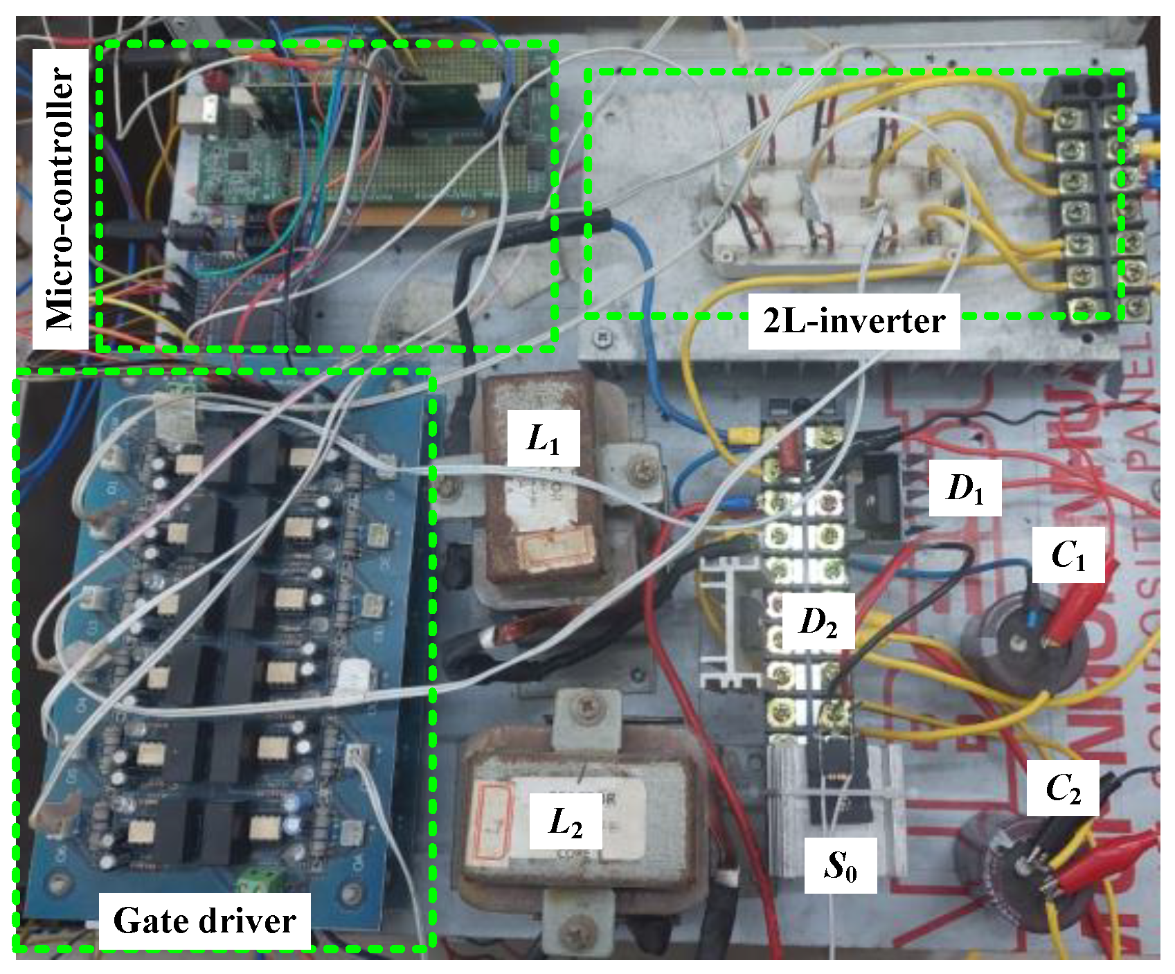
2. Proposed Active DC-Link Type Quasi-Z-Source Inverter (ADC-qZSI) Topology
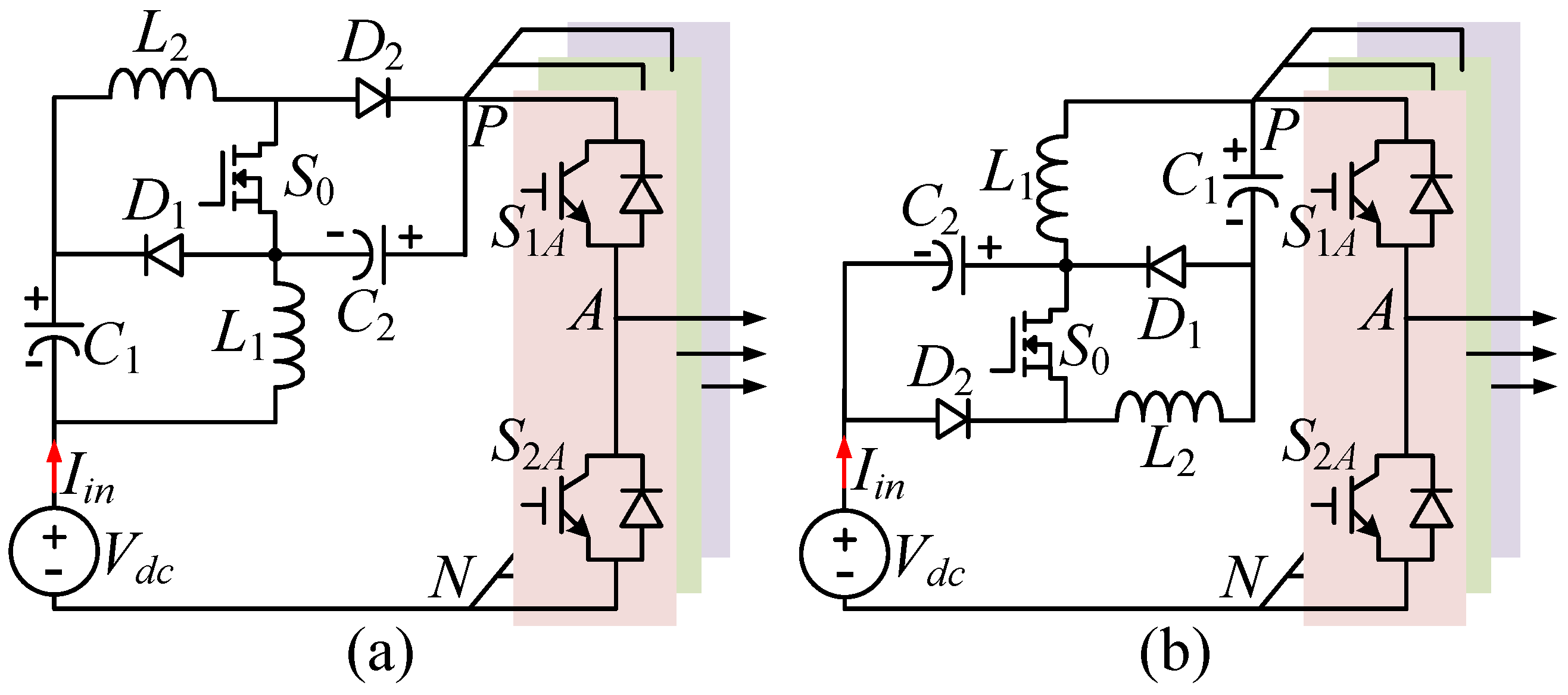
Two types of proposed ADC-qZSIs have been drawn in
Figure 1. Both types are constructed by an ADC-qZS network followed by a conventional two-level inverter. The impedance source network is known as the boost unit and is formed by two inductors (
L1 and
L2), two capacitors (
C1 and
C2), one active switch (
S0), and two diodes (
D1 and
D2). Compared to traditional DC-link qZSI in [
8], the proposed inverter has one extra active switch,
S0, and one extra diode,
D2. This insertion makes this topology flexible to control and increases the boost factor and voltage gain of the inverter. The conventional two-level inverter is responsible for buck operation. With the corresponding control method, the proposed inverter can buck and boost the output voltage from a single DC source,
Vdc. Each leg of the inverter side consists of two active switches,
S1X and
S2X, which ensures a two-level voltage at the output terminals, +
VPN and zero. In general, two types of ADC-qZSIs have similar operations, thus, type 1 shown in
Figure 1a is selected for analysis.
2.1. Operating States
Like any single-stage inverter, the ADC-qZSI is also proposed to operate under ST mode and non-ST mode, as shown in
Figure 2. The on/off states of inverter switches and diodes are listed in
Table 1.
In the ST state, as shown in
Figure 2a, the inverter side is able to produce value of 0 V at three-phase output voltages by turning on two switches in one phase leg, while switch
S0 is gated off. As a result, the DC-link voltage,
VPN, is shorted and has a value of zero. This ST state reverses diode
D1 and forward diode
D2 of impedance source circuit. In this mode, inductor
L1 is stored energy from DC input voltage and capacitor
C2, while inductor
L2 is stored energy from DC input voltage and capacitor
C1. The inductor voltages and capacitor currents are expressed as follows:
where
Vdc is DC input source;
VC1 and
VC2 are capacitor
C1 and
C2 voltages;
iL1,
iL2, and
iPN are instantaneous values of inductor currents and equivalent inverter side current.
In non-ST mode, the DC-link voltage obtains maximum value, which is determined by the summing DC input source and two capacitor voltages. With one extra switch,
S0, the non-ST mode consists of two sub-modes depending on the state of
S0. When
S0 is gated on, non-ST mode 1 shown in
Figure 2b is achieved. Diode
D2 is reversed bias, whereas diode
D1 is forward bias. It results in shorting inductor
L2 and discharging capacitor
C2. While capacitor
C1 is charged from inductor
L1. The following equations are obtained:
It can be seen that this non-ST mode maintains the energy of inductor L2 instead of discharging like conventional ISI, which increases the boost factor of the inverter.
Non-ST mode 2 of the proposed inverter, as shown in
Figure 2c, is like any single-stage inverter. Switch
S0 is gated off, whereas the inverter side switches operate like conventional inverters. Two inductors transfer energy to capacitors. The following equations are achieved:
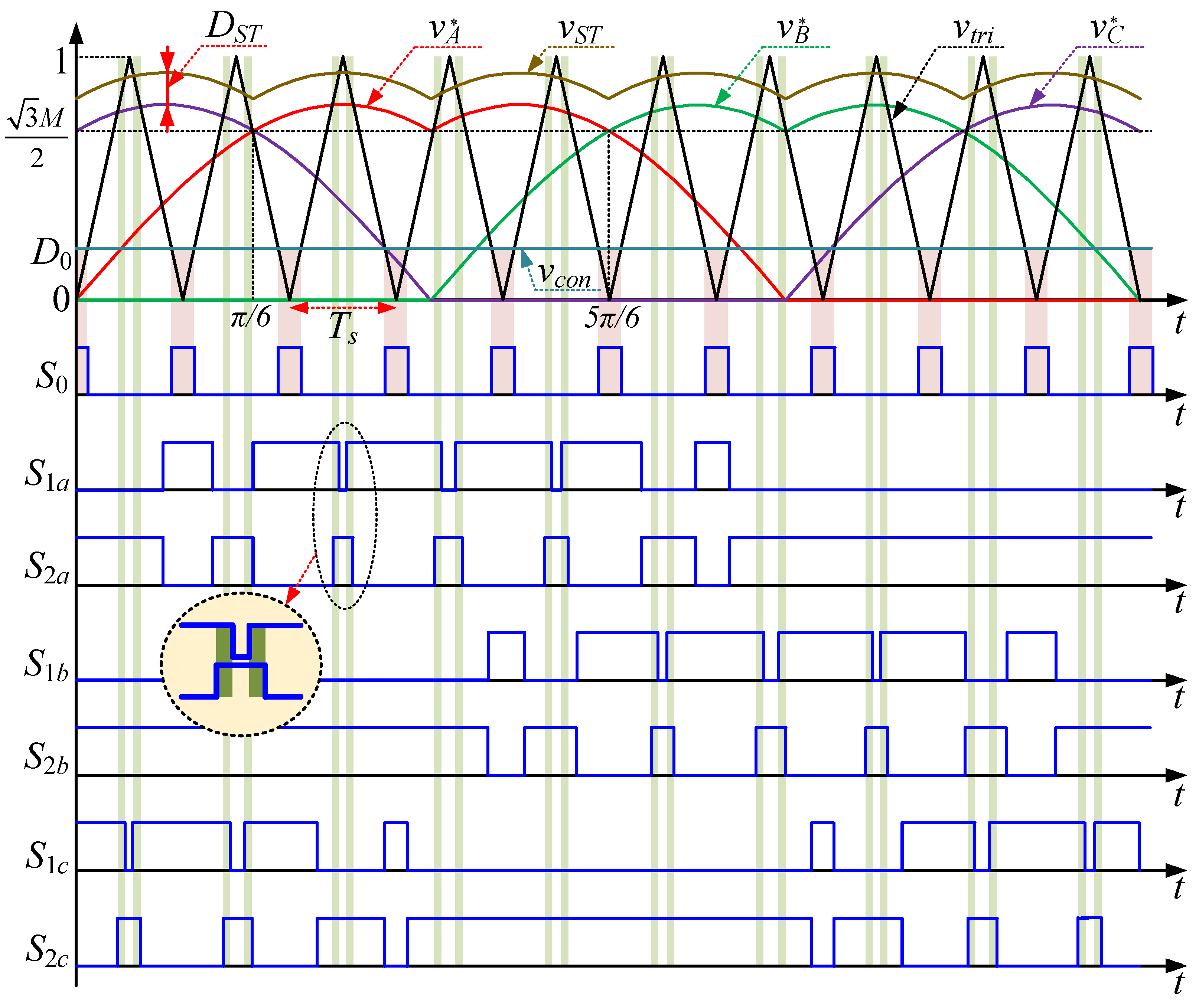
2.2. Proposed DPWM Control Strategy
To reduce the switching commutation, the proposed method uses a DPWM strategy to generate the control signals to inverter switches. To detail this modulation method, let us first define three signals
vX (
X =
A,
B, and
C) as follows:
where
M is modulation index;
fo is fundamental frequency.
Three reference signals
(
X =
A,
B,
C), as shown in
Figure 3, can be obtained by subtracting
vX from minimum value of
vA,
vB,
vC as follow:
These three reference signals are compared to high-frequency carrier
Vtri like a conventional two-level inverter, to produce on/off switching signals for inverter side switches. In this scheme, one-third of the output period has no switching commutation in any phase leg, as shown in
Figure 3. Thus, the switching loss can be reduced when compared to the conventional sinusoidal PWM method.
In the conventional PWM control method for single-stage inverters, the constant signal is used to generate the ST signal of the inverter leg. When this ST signal is inserted into the switching sequence, it produces at least two extra commutations in any phase leg. To overcome this, the proposed method uses discontinuous modulation signal
vST and the maximum value of
to produce ST signal, as presented in
Figure 3. In more detail, the ST signal is activated when
≤
Vtri ≤
vST. Then, this ST signal is inserted into the phase which has the maximum value of reference signal
by triggering on both switches
S1X and
S2X of that phase leg. In this way, the ST insertion does not generate any extra switching commutation compared to conventional two-level VSI. For example, as shown in zoom-in waveforms of switches
S1A and
S2A control signals, there are only two switching commutations for each switch, which equals the conventional two-level inverter.
Like any impedance source two-level inverter, the ST state must be inserted within zero vectors. Therefore, ST duty ratio
DST is not larger than (1 −
M) and can be controlled independently by
M. The
vST signal and ST duty ratio are expressed as follows:
where
DST is ST duty ratio.
The control signal of
S0 is generated by comparing control signal
vcon to carrier signal
Vtri, as shown in
Figure 3. The
vcon is identified as:
where
D0 is duty ratio of switch
S0.
In order not to affect the operating modes of the inverter,
vcon must be satisfied with the following term:
2.3. Steady-State Analysis
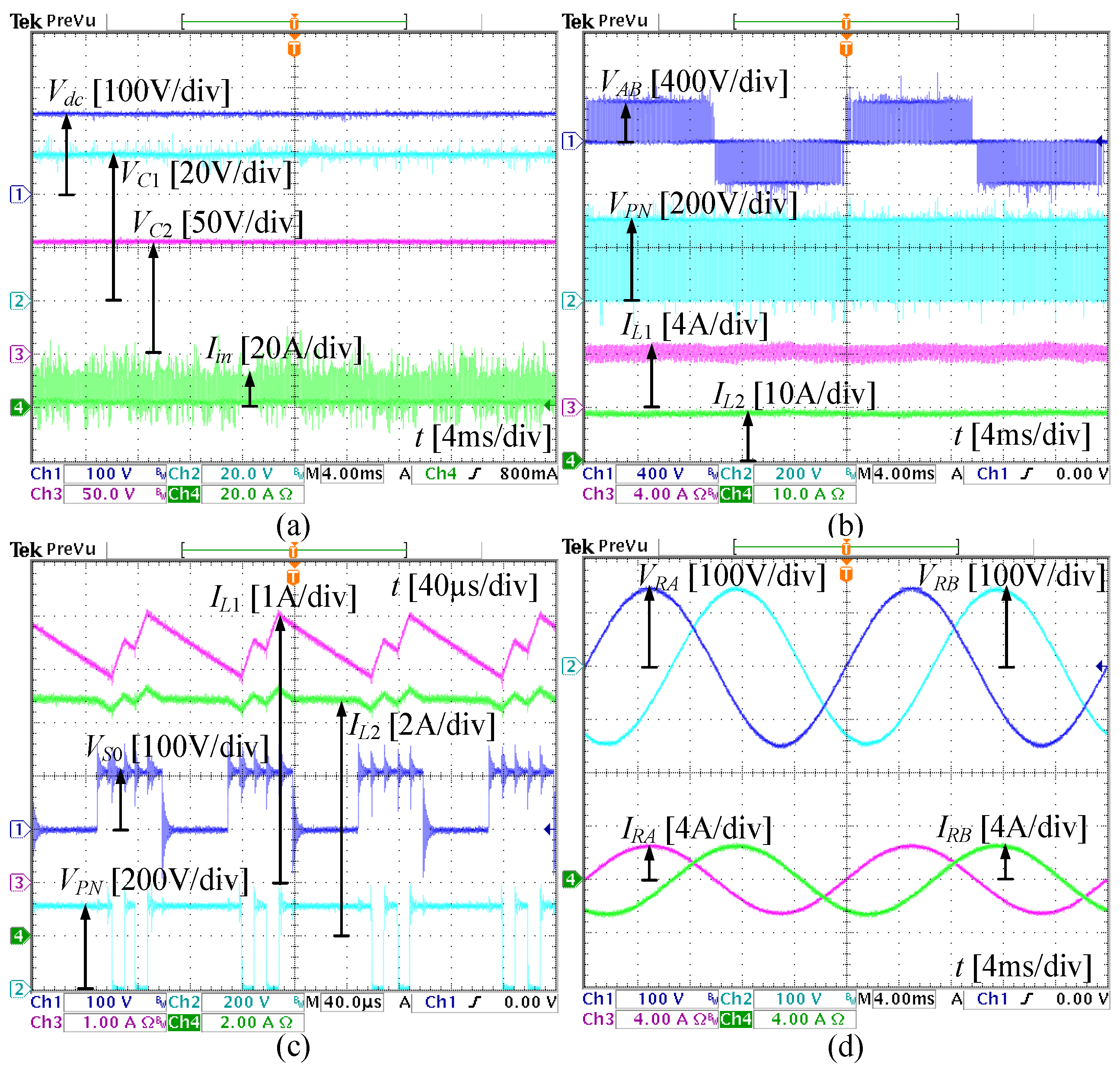
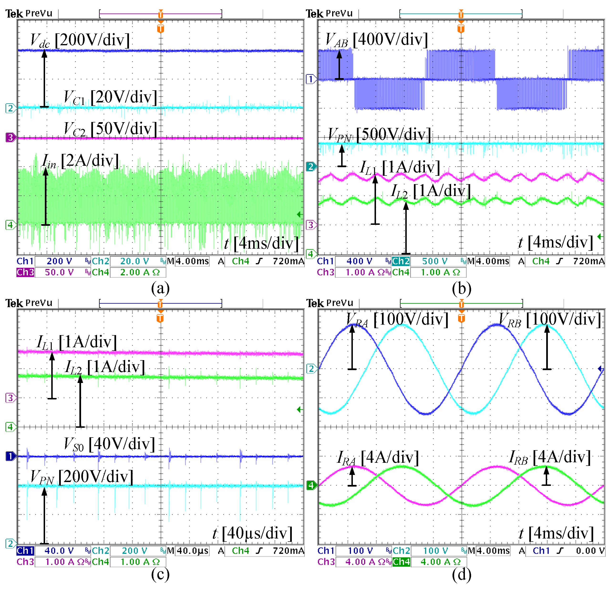
Figure 4 shows the profiles of inductor currents and capacitor voltages under one switching period,
Ts. It is clear that the total time of ST mode is
DST∙
Ts for any period
Ts. The time interval of non-ST mode 1 is equal to the on-time of switch
S0 which is determined as
D0∙
Ts. The rest time of
Ts is (1 −
DST −
D0)∙
Ts, which is the time interval of non-ST mode 2. By applying the volt-second balanced principle to two inductors,
L1 and
L2, the capacitor and DC link voltages can be identified as:
Assuming that the equivalent inverter current,
iPN, is constant, the average values of inductor currents can be approximately calculated by applying capacitor charge-balanced principle to capacitor
C1 and
C2 currents, as follows:
The boost factor,
B, of the inverter is identified as:
The peak value of fundamental component of output phase voltage is calculated as:
where
is the peak value of output phase voltage.
The voltage gain,
G, of proposed inverter is expressed as:
By setting D0 to max value which is expressed in (8), the max voltage gain can be obtained.
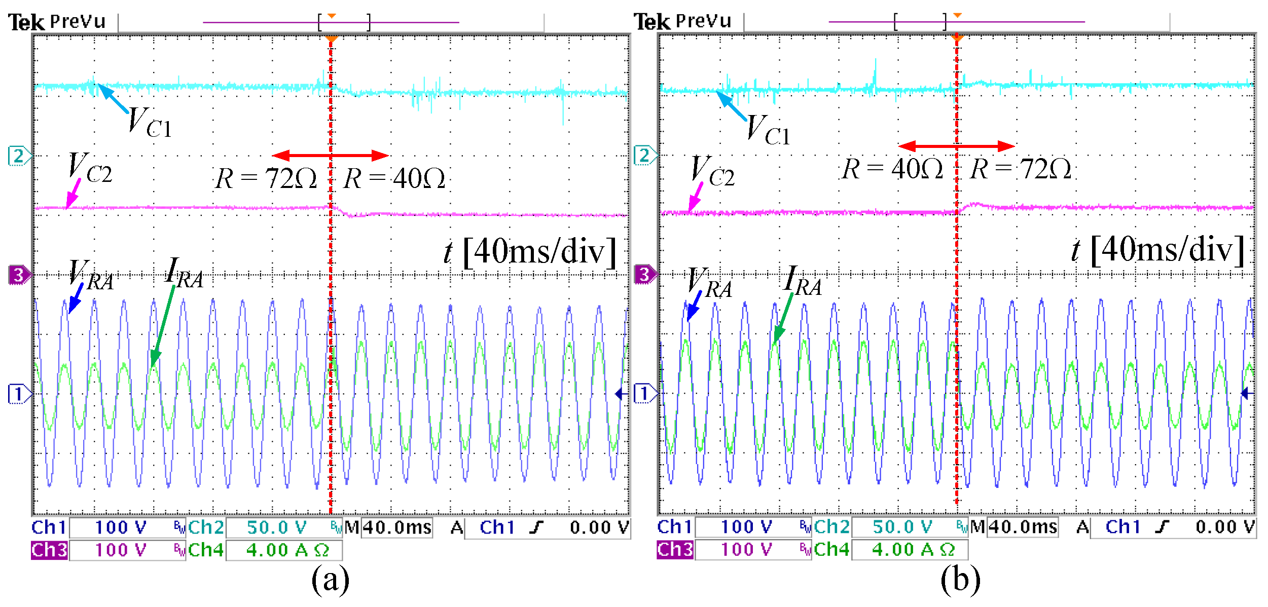
5. Comparison Study
The main contributions of the proposed configuration can be listed as (1) using a small number of passive components, (2) high voltage gain, and (3) low component voltage rating, which are verified by comparing to some previous single-stage inverters such as conventional DqZSI in [
8], SL-qZSI in [
18], rSL-qZSI in [
19], ASC-EqZSI in [
20], ASC/SL-qZSI in [
21], and HG-qSBI in [
22]. The comparison study concludes three sub-sections, which are (1) the number of components comparison; (2) boost factor and voltage gain comparison, and (3) component voltage stress comparison. Note that the proposed ADC-qZSI has two coefficients (
D0 and
DST) to control the boost factor. Their relationship is shown in (6) and (8). Thus, in this comparison study, both maximum boost and minimum boost control are considered. In detail, the maximum boost control can be obtained by setting the value
for
D0, and the minimum boost control can be achieved by setting the zero value for
D0. It is worth noting that the ST duty ratios,
DST, of these works are set as (1 −
M).
5.1. Number of Components
The overall comparison between these configurations has been summarized in
Table 3. Among these topologies, the conventional DqZSI topology in [
8] uses the smallest number of elements compared to others. However, it makes conventional topology have lower voltage gain and higher voltage stress compared to others, which is detailed in the next section. The SL-qZSI in [
18] and rSL-qZSI in [
19] do not use active switching devices in impedance source networks. Instead, they use more inductors and diodes to enhance voltage gain. In detail, the SL-qZSI in [
18] uses one more inductor and two more diodes, while the rSL-qZSI in [
19] uses two-more inductors and five more diodes compared to the proposed ADC-qZSI. The use of active switches in intermediate network topologies like [
20,
21,
22] and the proposed topology helps save a large number of passive components like inductors and capacitors. The work in [
21] uses two fewer inductors, one fewer capacitor, and two fewer diodes than in [
19]. However, it still utilizes three more diodes than the proposed ADC-qZSI. Moreover, the use of only one capacitor [
21] causes high capacitor voltage stress, which is detailed in the next part of this section. The proposed topology has the same number of components as ASC-EqZSI in [
20] and HG-qSBI in [
22], which are two inductors, two capacitors, two diodes, and only one active semiconductor device in the impedance-source network. Note that the inverter sides of these configurations use a conventional two-level inverter, thus, the number of elements for the inverter side circuit is the same for all these topologies.
5.2. Boost Factor and Voltage Gain
The boost factor and voltage gain of these topologies are shown in
Figure 6. According to some studies [
18,
19,
20,
21,
22], the HG-qSBI in [
22] has the largest boost factor, as presented in
Figure 6a, thus it also has the largest voltage gain. When the minimum boost control is applied, the boost factor of the proposed inverter is 1/(1 − 2
DST), which is equal to conventional qZSI in [
8]. As a result, the proposed topology produces the smallest boost factor and voltage gain compared to the works in [
18,
19,
20,
21,
22]. However, the boost factor of the proposed ADC-qZSI can be extended by increasing the duty ratio
D0 of switch
S0. When the duty ratio
D0 obtains a value of 0.5, the boost factor and voltage gain of the proposed method are equal to HG-qSBI in [
22] and also higher than the works in [
18,
19,
20,
21]. When the maximum value of
D0,
, is achieved, the boost factor and voltage gain of the proposed ADC-qZSI are the largest, which brings a benefit to the low component voltage rating, as follows.
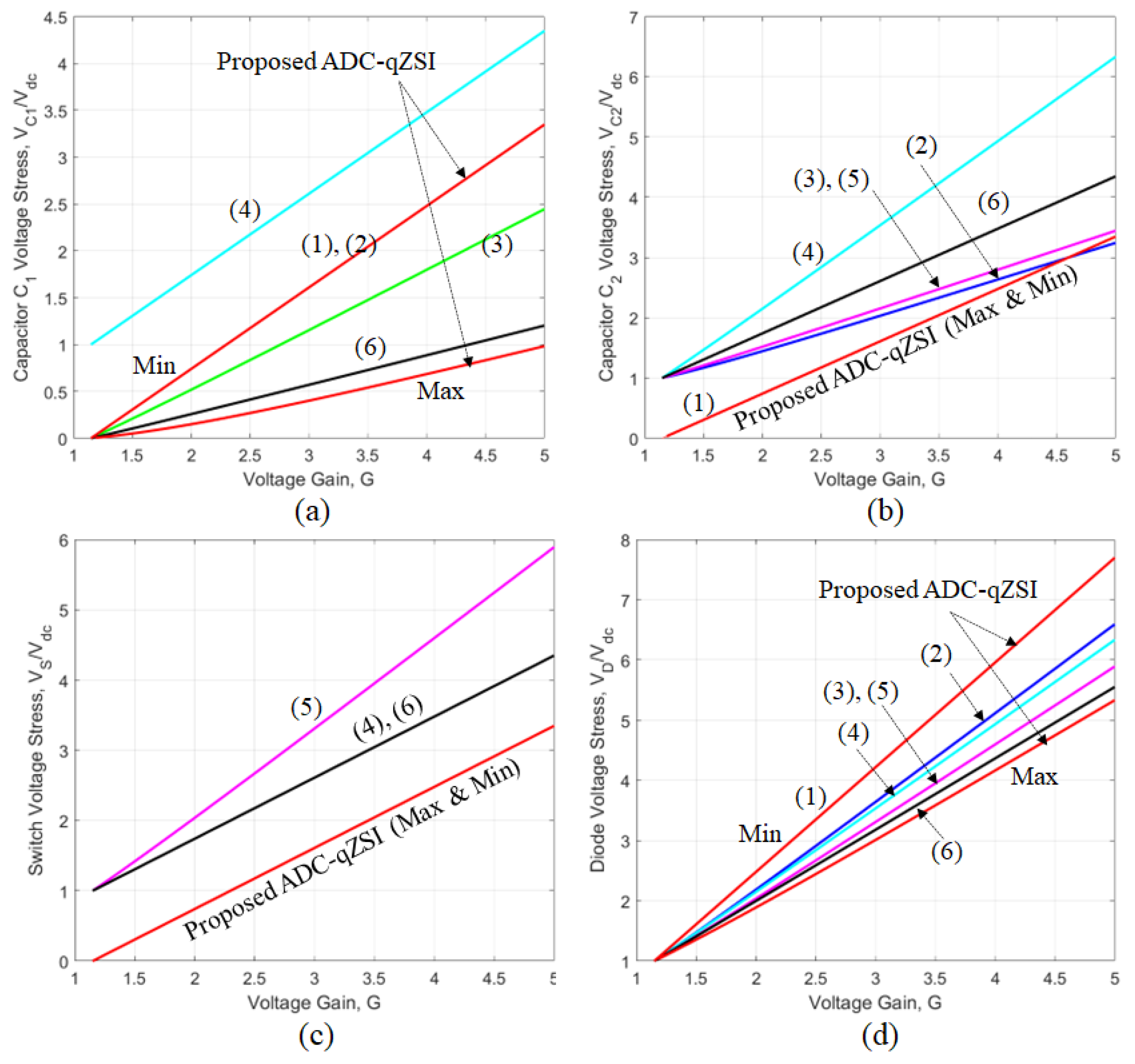
5.3. Component Voltage Rating
Some investigations on capacitor, diode and switch voltage stresses have been conducted, as illustrated in
Figure 7. Note that there are a lot of diodes in these topologies, which have unequal voltage stresses, as shown in
Table 3. Therefore, simply, the maximum values of diode voltage stresses are only considered in this comparison study.
Figure 7a,b show voltage stress comparisons for capacitors
C1 and
C2. The max boost control of the proposed ADC-qZSI produces the smallest capacitors
C1 and
C2 voltage rating compared to others, as shown in
Figure 7a,b. Among these topologies, the impedance-source switch voltage stress is equal to the capacitor voltage. Thus, having a lower capacitor voltage rating causes a lower switch voltage rating, as shown in
Figure 7c.
Having a higher voltage gain makes the proposed ADC-qZSI able to use a higher modulation index compared to other topologies, as shown in
Figure 6b. On the other hand, the boost factor can be calculated as follows:
From (23), it can be seen that the proposed topology with the introduced DPWM method uses a higher modulation index, which leads to requiring a lower boost factor. The max value of diode voltage stress equals the boost factor, as shown in
Table 3. Moreover, it is clear that the inverter side switch voltage rating is also equal to the boost factor. As a result, the proposed ADC-qZSI has the lowest diode and inverter side switch voltage stresses among these configurations, as presented in
Figure 7d.


