Article

Fast DC Fault Current Suppression and Fault Ride-Through in Full-Bridge MMCs via Reverse SM Capacitor Discharge

by
Munif Nazmus Sakib
,
Sahar Pirooz Azad
* and
Mehrdad Kazerani
Electrical and Computer Engineering, University of Waterloo, 200 University Ave. W., Waterloo, ON N2L 3G1, Canada
*
Author to whom correspondence should be addressed.
Energies 2022, 15(13), 4595; https://doi.org/10.3390/en15134595
Submission received: 2 May 2022 / Revised: 11 June 2022 / Accepted: 20 June 2022 / Published: 23 June 2022
(This article belongs to the Section F3: Power Electronics)

Abstract

:
In the event of a DC side fault in modular multilevel converters (MMCs), the fault current contributions are initially made by submodule (SM) capacitor discharge, which occurs before the fault is detected, followed by the AC side contribution to the DC side fault. While the AC side currents can be regulated using fault blocking SMs, the initial discharge of the SM capacitors results in high DC fault currents, which can take several milliseconds to be brought under control. This paper presents a method to actively control the rate of rise of the DC fault current by regulating the discharge of SM capacitors and accelerating the suppression of fault current oscillations during fault ride-through (FRT) in a full-bridge (FB)-MMC system. In the proposed method, the discharge direction of the FBSM capacitors is reversed following the detection of a DC side fault, which leads to a reversal in the fault current direction and a fast drop-off towards the zero-crossing. Immediately after the zero-crossing of the DC fault current, the DC fault is cleared by adjusting the arm voltage references and operating the MMC as a static synchronous compensator (STATCOM) to provide voltage support to the AC grid. The proposed control scheme provides faster fault current suppression, more effective SM capacitor voltage regulation, low AC side and MMC arm current transient peaks, and an overall superior DC-FRT performance compared to methods in which the conventional fault ride-through operation is initiated immediately upon DC fault detection.

1. Introduction

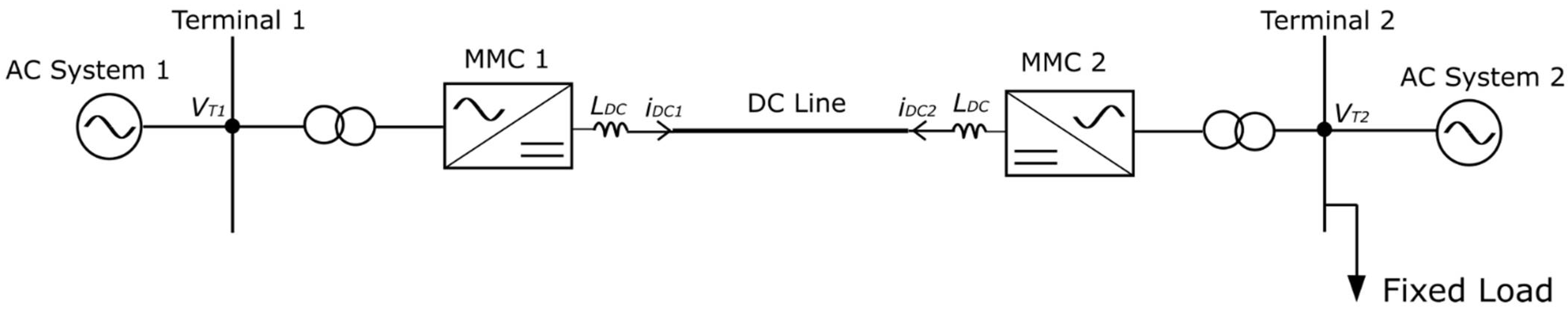
High voltage direct current (HVDC) is more cost-effective than high voltage alternating current (HVAC) for transmitting power over long distances, and therefore is ideal for bulk power transfer from wind, solar, hydroelectric, and tidal power plants located in offshore or in remote locations to load centers [1]. The use of voltage-sourced converters (VSCs) in HVDC transmission systems offers greater flexibility when compared to their counterpart, line commutated converters (LCCs), due to their smaller footprint, improved power quality, as well as decoupled active and reactive power control, voltage support, and black start capabilities [2]. The most recent advancements in VSC technology have led to the emergence of a new converter topology known as the modular multilevel converter (MMC) [3]. The simplest and most economical MMC cell structure is the half-bridge submodule (HBSM), which is unable to prevent AC side contribution to DC side faults in HVDC systems. Therefore, DC fault protection in the HB-MMC requires either installation of expensive DC circuit breakers (DCCBs) [4] or the opening of AC side breakers that are not adequately fast [5]. Adding two extra switches to the HBSM results in the full-bridge submodule (FBSM) configuration, which ensures that, in the event of a DC side fault, there is a reverse voltage in the path of the AC side current feeding the DC side fault through the antiparallel diodes in the SM switches [6]. Furthermore, instead of blocking the fault current, certain fault-tolerant SMs may also be utilized as wave-shaping circuits to control the AC currents during the fault and provide reactive power support to the grid, thereby enabling the MMC to work as a static synchronous compensator (STATCOM) [7].
A DC side fault event in MMC-HVDC systems can be divided into two stages [8]. In the first stage, the MMC can generate the AC side voltages and therefore the AC side currents remain controlled. As a result, the fault current in the first stage consists mainly of a DC component due to the discharge of the SM capacitors. There is also another DC component in the fault current due to the discharge of the transmission line distributed capacitance. However, the line capacitance and therefore its contribution to the fault current is negligible compared to that of the MMC capacitors [9]. The main consequence of the discharge of SM capacitors is that the MMC can no longer generate the AC side voltages and starts to lose control of the AC side currents. Therefore, in the second stage, the AC side starts contributing to the fault; thus, there will be an AC component in the fault current in addition to the DC component. Since the capacitors are the main source of the DC fault current during the initial stage, manipulation of the SM capacitor discharge rate would be an effective means of limiting the DC fault current, especially in HB-MMC systems that are incapable of blocking or riding through DC faults.
A few methods involving SM capacitor discharge control in HB-MMC systems, to achieve fault current control, have been proposed in the literature. One approach is to block the IGBTs and prevent SM discharge completely. Such an action would eliminate the SM capacitor contribution to the fault, but the diode freewheeling effect in HBSMs means the DC fault current, even though reduced, would not be completely suppressed [8]. A significant disadvantage of the blocking action is that it would cause overvoltage across the arm inductors [10]. Another approach is to bypass the SMs entirely by using either the SM IGBTs [11] or double thyristor switches connected in parallel with the SMs [12]. The purpose of installing thyristors in parallel to the SMs is to protect the IGBTs from sustained high levels of fault current; thyristors typically have much higher current ratings than IGBTs. However, this bypassing action would transform the DC side short circuit into an AC short circuit and will lead to an overcurrent on the AC side and in the MMC arms. Such deficiencies in both blocking and bypass approaches have necessitated the development of new methods [13,14] that can provide a degree of control over the SM capacitor discharge rate.
As mentioned earlier, some SMs are capable of either blocking the DC fault current or riding through the DC fault while the MMC is operated as a STATCOM. Fault blocking SMs that are unipolar [15,16] are usually capable of only the former function while bipolar SMs [17,18] can achieve both functionalities [19]. Even though the blocking action realized by fault-tolerant SMs to facilitate fault current suppression can be achieved very quickly (usually within a few milliseconds) [20], it would prevent the converter from working as a STATCOM and provide voltage support at the point of common coupling (PCC). Meanwhile, bipolar SMs such as the FBSM are capable of clearing DC faults and simultaneously allowing the MMC to operate as a STATCOM to provide reactive power support [7] to the AC side. However, it can take tens of milliseconds for the fault current to decay to zero after clearance of the DC fault and initiation of the STATCOM mode, due to the slow damping of the fault current by the DC transmission line [21]. A damping method based on utilizing an active resistance to absorb the inductive energy and accelerate DC fault current suppression was briefly discussed by the authors of [21]. However, no details on the active resistance calculation method were provided. In [22], a novel SM capacitor energy balancing strategy was proposed that has the added advantage of reduced oscillations in the fault current during DC side faults. However, the proposed strategy is complex to implement. A DC FRT strategy with independent pole control is proposed in [23]. However, the strategy is only meant for utilization during pole-to-ground faults. No other notable techniques to decrease oscillations and enable faster DC fault current suppression were found in the literature. To summarize, the existing literature focuses on (i) DC FRT capability of fault-tolerant MMC topologies while working as STATCOMs to provide reactive power support to the grid, and (ii) fault blocking schemes for fault-tolerant MMC topologies that enable fast suppression of DC fault currents. The main shortcoming associated with the first approach is the relatively slow fault current interruption, while the drawback of the second approach lies in its inability to provide reactive power support to the grid leading to voltage instability. This paper attempts to address the gap in research on fast DC fault current suppression techniques during STATCOM operation of MMCs by introducing a new control scheme that can be utilized in fault-tolerant MMC configurations to ride-through DC faults and provide voltage support to the AC grid.
The proposed control scheme of this paper is inspired by [14,24], but in contrast to that of [14,24], it facilitates fast DC fault current suppression and enables the provision of reactive power to the AC grid during DC side faults. In [14,24], the authors focused on the manipulation of DC fault current rate of rise by controlled SM capacitor discharge in HB-MMC systems. The purpose was to reduce the rate of rise of the DC fault current such that the size of the DC line reactors could be decreased, leading to lower costs. Since reduced SM capacitor discharge would by no means facilitate DC fault current suppression, such a method would not be useful in MMC-HVDC systems comprising fault-tolerant SMs capable of either blocking the DC fault current or riding through the DC faults while operating as STATCOMs. The purpose of this paper is to modify the fault current limiting technique of [14], which is only applicable to HB-MMC systems, in a way that it could be implemented in fault-tolerant MMCs to enhance DC-FRT performance. To achieve this goal, a state-space averaging approach that can be utilized in bipolar SM-based MMC systems is developed. Theoretical underpinnings of the proposed control method are presented and simulation results confirming its superior performance in riding through DC faults and suppressing fault current oscillations, compared to the conventional operation of fault-tolerant MMCs as STATCOMs, are provided.

2. MMC Structure and Control

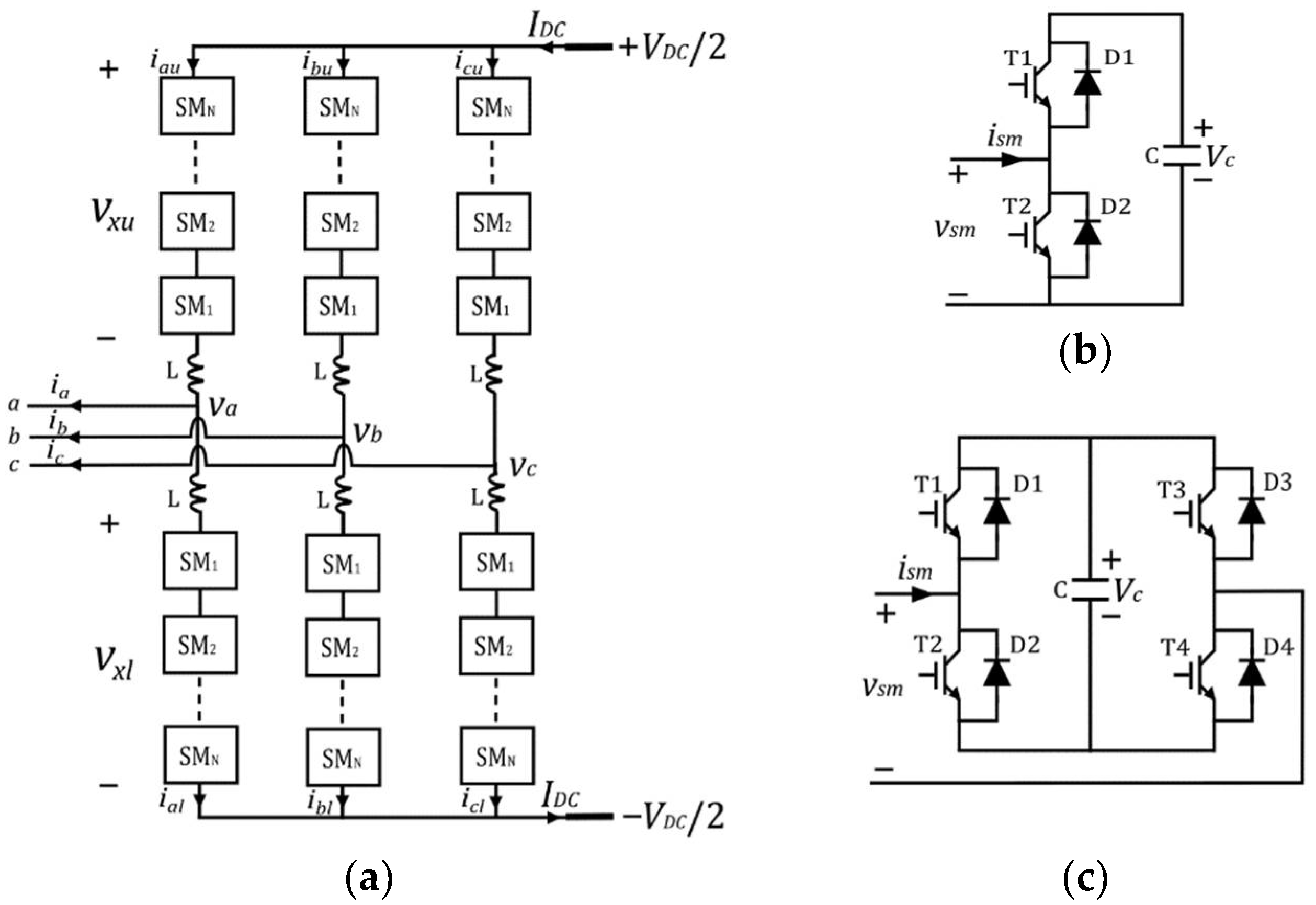
The generic structure of a three-phase MMC is shown in Figure 1a. Each arm of the converter comprises N series-connected SMs along with an inductor. The phase x terminal voltage, v x (xa, b, c) in Figure 1a, may be expressed in either one of the following ways,
v x = V D C 2 v x u L d i x u d t ,
v x = V D C 2 + v x l + L d i x l d t ,
where v x u and v x l denote the total upper and lower arm SM voltages, and i x u and i x l are the upper and lower arm currents in each phase. The arm currents ( i x u and i x l ) in each phase of the MMC, shown in Figure 1a, can be expressed as a combination of the AC output current i x and a common-mode current i x z , i.e.,
i x u = i x z + 1 2 i x ,
i x l = i x z 1 2 i x ,
where the common-mode current represents a combination of the DC bus current ( I D C ) and AC circulating current components. The DC part of the common-mode current is responsible for active power flow through the converter while the AC part, which is a negative sequence current, causes power loss in the converter and needs to be suppressed [25]. Traditional vector control methods [26] are commonly implemented in MMC-HVDC systems. Various modulation methods, such as the nearest level modulation [27] and high-frequency carrier-based sinusoidal pulse width modulation techniques [28] can be employed for the generation of the AC side waveforms. Since SMs contain capacitors, voltage balancing [29] and sorting algorithms [30] are also implemented to keep the capacitor voltages close to their nominal values.
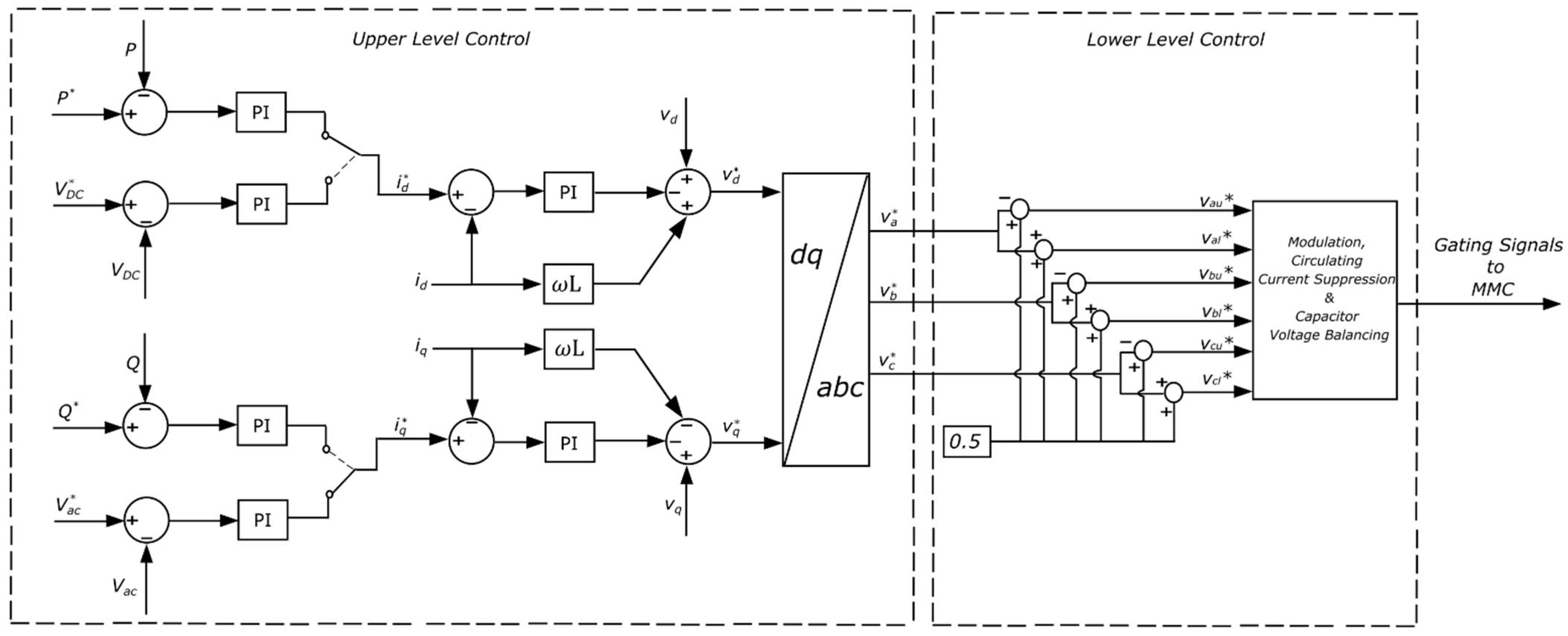
The control can be divided into upper- and lower-level controls. The upper-level controls (based on the traditional vector control methods) are further divided into two parts: outer control and inner decoupled current control. The outer controller consists of two control loops, both using proportional-integral (PI) control blocks. One loop controls either the active power (P) or the DC side voltage ( V D C ), while the other loop controls the reactive power (Q) or AC side voltage ( V a c ). These outer controllers generate d- and q-axis current references for the inner current control blocks, as shown in Figure 2. In the inner decoupled current controller, d- and q-axis current values ( i d , i q ) measured from the AC grid are regulated against their references ( i d * , i q * ) obtained from the outer controller by employing PI control. This generates the references for the d- and q-axis components of the AC voltage ( v d * , v q * ), which are then transformed to abc reference frame components ( v a * , v b * , v c * ). These voltages are then fed into the lower-level control system.
The lower-level control is responsible for modulation, circulating current suppression, and SM capacitor voltage balancing. Common modulation schemes include phase-shifted pulse width modulation [31], phase-disposition pulse width modulation [32], and nearest level control [33]. The primary component in the circulating current is of negative sequence at twice the fundamental frequency [34]. In [35], a controller is presented that can be utilized to suppress the circulating current primary component.
Continuous insertion and bypassing of SM capacitors inevitably leads to fluctuation in individual SM capacitor voltages [36]. The sorting algorithm described in [30] sorts the SM capacitor voltages in the order of magnitude. Then, depending on the arm current direction and the number of SMs to be inserted in the arm (determined in the modulation stage), SMs with the lowest (highest) voltage magnitudes are selected to be in the current path to be charged (discharged). Due to its simplicity, this method has gained widespread recognition.
The HBSM structure, depicted in Figure 1b, is capable of generating two voltage levels of 0 and V c . In contrast, FBSM, shown in Figure 1c, can generate three voltage levels: 0, V c and V c . Hence, the FBSM is a bipolar SM that can generate negative voltage states not only during DC fault blocking but also during regular operation, which is an essential feature when DC FRT capability is required in the converter.
While the blocking action by fault blocking modules suppresses the fault current very quickly, it would prevent the converter from operating as a STATCOM to provide voltage support at the PCC. Bipolar SMs, such as the FBSM, are capable of riding through DC faults, allowing the MMC to operate as a STATCOM and providing reactive power support. However, operation as a STATCOM requires modifications to the balancing approach employed in the arms and legs of the MMC [7]. Moreover, it can take several milliseconds for the fault current to decay to zero after the DC fault has been cleared through adjustments to the MMC arm voltage references. This is due to the low damping characteristics of the DC transmission line [21]. To facilitate fast DC fault current suppression, an approach based on the regulation of SM capacitor discharge is presented in the following sections.

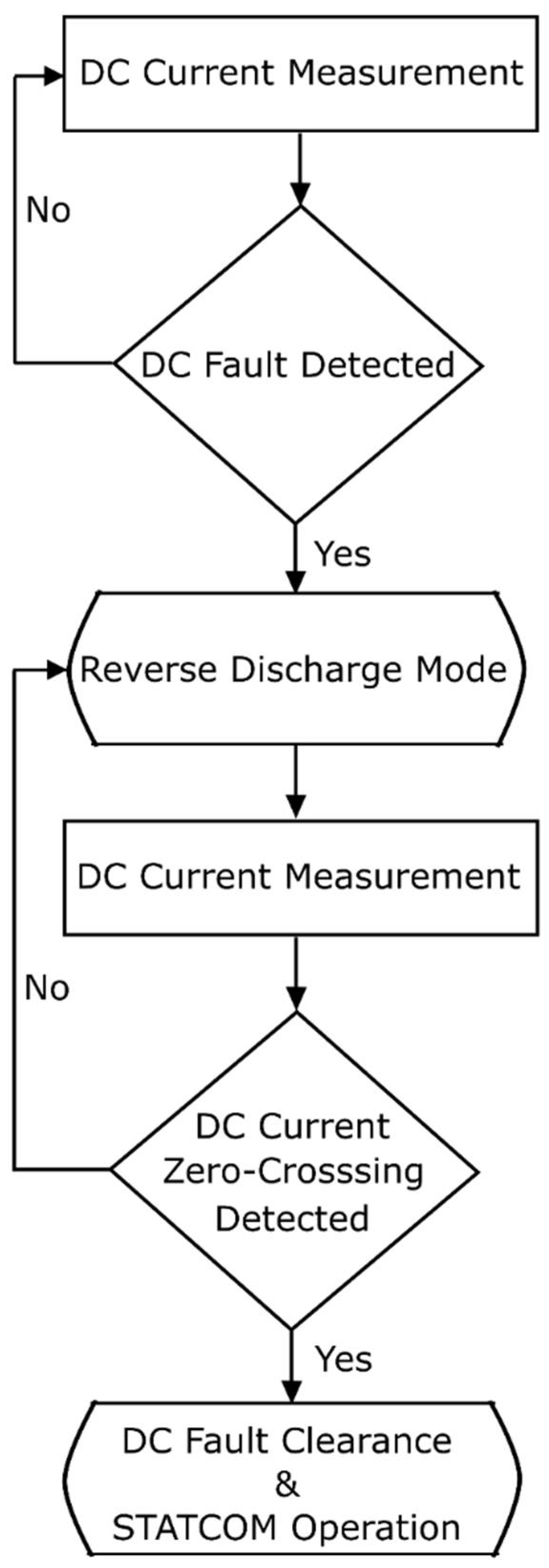
3. Submodule Capacitor Discharge Control & DC Fault Clearance

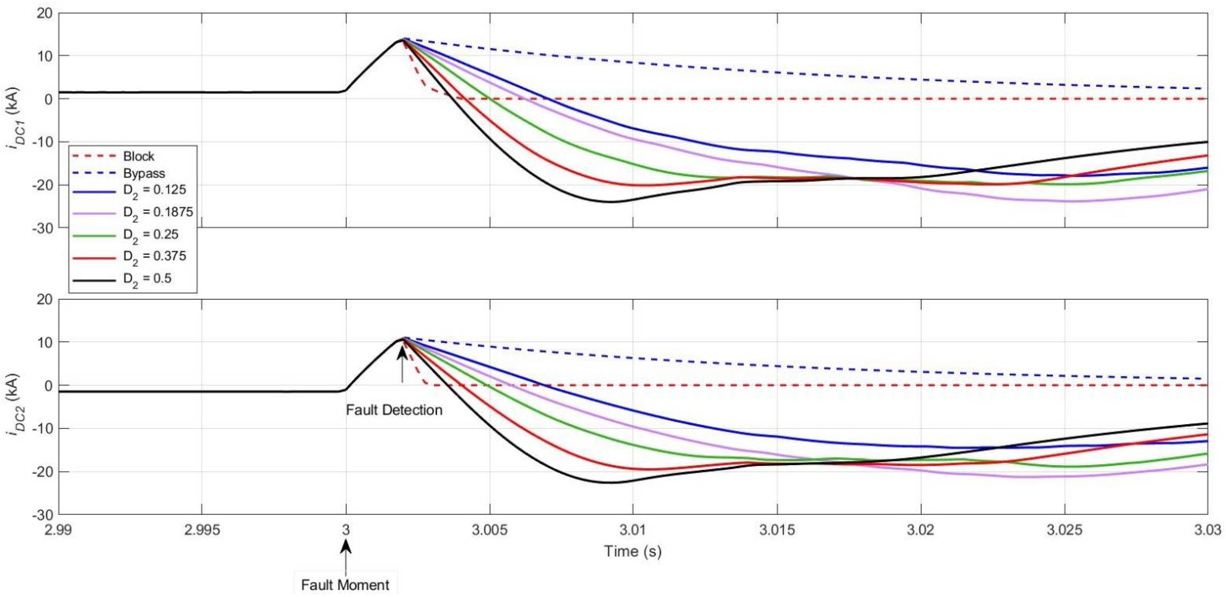
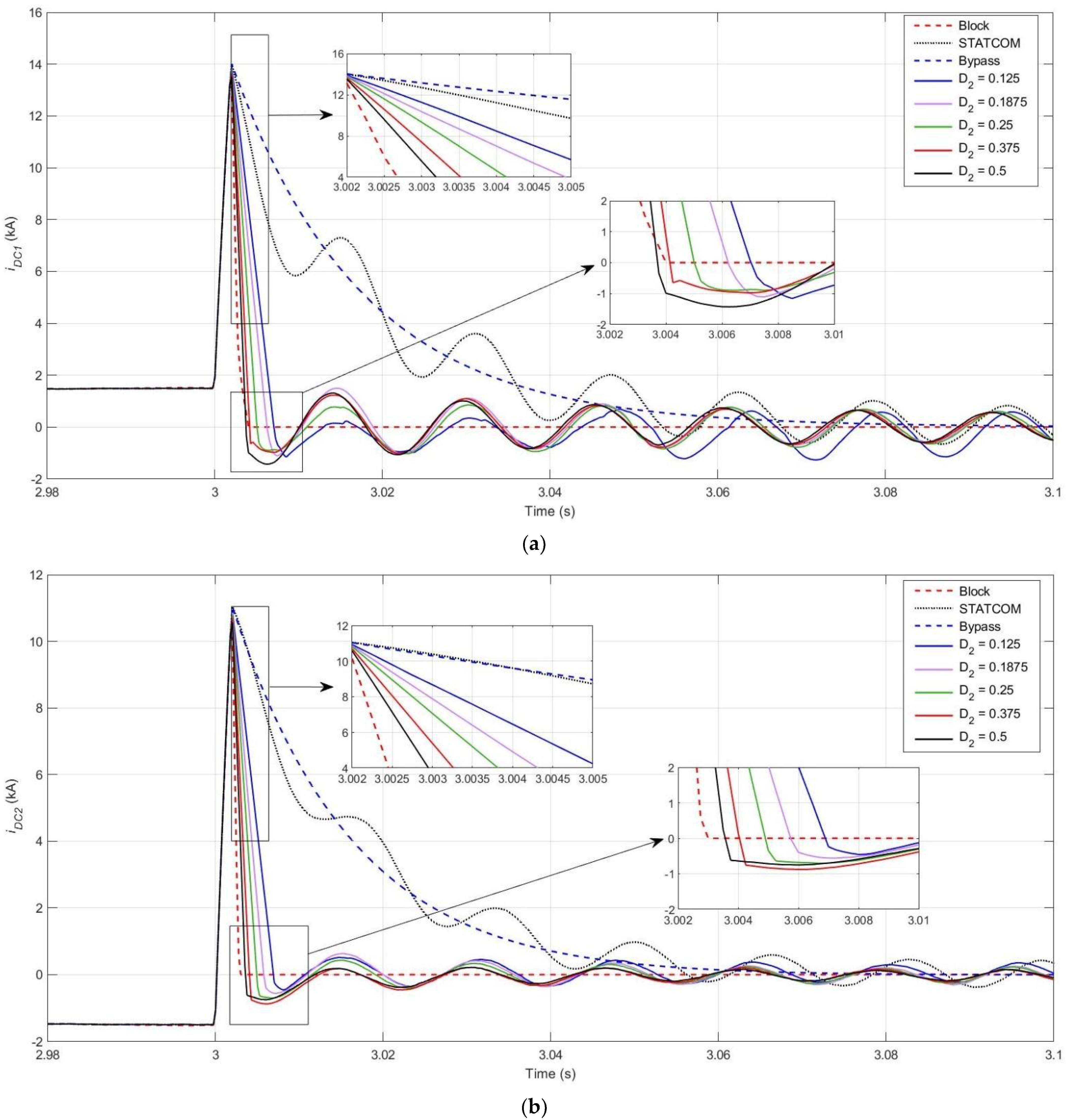
Each MMC arm inserts a certain proportion of N capacitors during each switching period. When a DC side fault occurs, before it is detected, the SM capacitors will discharge whenever they are inserted into the current path, leading to a rapid rise in the DC fault current. In an FB-MMC system, the two extra switches in the FBSM would allow the SM capacitors to be inserted in either polarity into the current path. Capacitor discharge would occur regardless of the insertion polarity, but the difference will be in the direction of the discharge current. If the extra switches in an FBSM are utilized to reverse the polarity of capacitor insertion immediately after DC fault detection, then this should result in a reversal of the direction of flow of fault current as well. Such a change in the direction of the DC fault current will inevitably result in a zero-crossing. The DC fault clearance and STATCOM operation of the MMC(s) can be initiated after detection of the zero-crossing, resulting in quick suppression of the fault current. The control method proposed in this paper is based on this specific idea.
Three independent base circuits, as depicted in Figure 3 can be used to represent the insertion/bypass states of the FB-MMC. Base circuit 1 represents the case when all SM capacitors are inserted in the circuit in the conventional direction, while base circuit 2 portrays the opposite scenario, i.e., when all SM capacitors are inserted in the reverse direction. Base circuit 3 represents the bypass state of the SMs. A variable D 1 can be defined to denote the duty cycle for base circuit 1 during each switching period, Ts, while D 2 represents the duty cycle for circuit 2. Either ( 1 D 1 ) or ( 1 D 2 ) is then the duty cycle for base circuit 3 depending on whether the SMs are being inserted in the conventional or the reverse direction. The capacitor insertions occur in only one specific direction within a switching cycle. Therefore, SM insertions can be accurately represented by utilizing either base circuits 1 and 3 or 2 and 3. It is not necessary to combine base circuits 1,2 and 3 to represent the state of discharge of the SM capacitors.
The variable D 1 represents the state of discharge of the SM capacitors in the conventional direction. Therefore, establishing control over the variable D 1 would enable direct control over SM capacitor discharge, and thus the DC fault current. Since D 1 is an insertion parameter, it can be expressed by the ratio of the sum of the upper and lower arm voltages in a phase divided by the total generation capacity of the two MMC arms,
D 1 = v x u + v l u 2 V D C .
Neglecting the voltage drop across the arm inductors, the arm voltage expressions in phase x are given by,
v x u = V D C 2 v x ,
v x l = V D C 2 + v x .
In the expression for D 1 , the AC terms in the arm voltages would cancel each other out during normal operation, implying that the value of D 1 will be equal to 0.5 in this case. Thus, D 1 is the normalized DC component of the arm voltage reference. Since D 1 is 0.5 during normal operation, controlled capacitor discharge, and subsequent fault current limiting action will be performed when it is varied between 0 and 0.5.
Likewise, the variable D 2 represents the state of discharge of the SM capacitors and is also an insertion parameter described by the same equation as used for D 1 , i.e.,
D 2 = v x u + v l u 2 V D C .
However, during reverse capacitor insertion, the arm voltage references given by (6) and (7) need to be modified as:
v x u = V D C 2 v x ,
v x l = V D C 2 + v x .
Once again, the AC terms cancel each other, and the nominal value of D 2 is −0.5. However, the MMC is never operated in this mode during regular operation since it would lead to a reversal in the DC link polarities. The only possible benefit of operation in the reverse region would be to bring about a change in the DC fault current direction after the onset of a DC side fault. With that in mind, it is essential to derive expressions relating   D 2 with the DC fault current.
The DC fault current i D C (reactor current) and the averaged SM capacitor voltage u C can be chosen as state variables in the state vector x 1 ( t ) . Since the DC fault transient is short (a few milliseconds), the voltages of SM capacitors are assumed to remain balanced. Then, the individual SM capacitor voltage u C can be used to represent the capacitor energy stored in the MMC. The state vector x 1 ( t ) can be expressed as:
x 1 ( t ) = [ i D C ( t ) u C ( t ) ] .
In [14], a relationship between i D C and D 1 was derived by utilizing the state-space representation of base circuits 1 and 3. However, the focus of this paper is on reverse discharge control involving base circuits 2 and 3. The reason is that the reverse discharge control, which is specific to bipolar SMs, results in a zero-crossing. The detection of zero-crossing is used as an indicator during DC FRT to initiate fault clearance and STATCOM operation in the MMC(s), thereby enabling fast DC fault current suppression. To that end, a second variable i D C R for the DC fault current is introduced whose direction is opposite to that of i D C , as shown in Figure 3. The discharge of the capacitor, controlled by the duty cycle D 2 would then affect i D C R in the same manner as D 1 influences i D C . Another state vector x 2 ( t ) in terms of i D C R and u C can then be defined as:
x 2 ( t ) = [ i D C R ( t ) u C ( t ) ] .
In this paper, x 2 ( t ) rather than x 1 ( t ) is selected as the state vector to maintain similarity between the two derivation processes. For a switching period denoted by T s , the span of the first subinterval corresponding to base circuit 2 with all capacitors inserted in the reverse direction would be D 2 T s . The length of the second subinterval with all capacitors bypassed, as depicted in base circuit 3, would then be ( 1 D 2 ) T s . Applying Kirchhoff’s voltage and current laws (KVL and KCL) in base circuit 2, the following expressions involving the state variables can be obtained,
2 N u C ( t ) L e d d t i D C R ( t ) R e i D C = 0 ,
C e d d t { 2 N u C ( t ) } + i D C R ( t ) = 0 ,
where N is the number of SMs per arm, L e is the equivalent inductance, R e refers to the equivalent resistance, and C e denotes the equivalent capacitance, given by (15)–(17), respectively,
L e = 2 L s 3 + L D C ,
R e = 2 R s 3 + R f ,
C e = 3 C d 2 N .
Similar expressions can be derived for base circuit 3, by applying KVL and KCL, as:
L e d d t i D C R ( t ) R e i D C R = 0 ,
C e d d t u C ( t ) = 0 .
The state-space expressions for base circuits 2 and 3, in matrix form, are given by (20) and (21), respectively,
[ L e 0 0 C e ] d d t [ i D C R ( t ) u C ( t ) ] = [ R e 2 N 1 2 N 0 ] [ i D C R ( t ) u C ( t ) ] ,
[ L e 0 0 C e ] d d t [ i D C R ( t ) u C ( t ) ] = [ R e 0 0 0 ] [ i D C R ( t ) u C ( t ) ] .
To combine the two sets of state-space equations, an averaged matrix R can be derived, based on the duty cycles of the two base circuits, as:
R = D 2 R 1 + ( 1 D 2 ) R 2 = [ R e 2 N D 2 D 2 2 N 0 ] ,
where,
R 1   = [ R e 2 N 1 2 N 0 ] ,
R 2   = [ R e 0 0 0 ] .
The complete time-averaged expression can now be expressed as,
[ L e 0 0 C e ] d d t [ i D C R ( t ) T s u C ( t ) T s ] = [ R e 2 N D 2 D 2 2 N 0 ] [ i D C R ( t ) T s u C ( t ) T s ] ,
where i D C R ( t ) T s and u C ( t ) T s are time averages of i D C R and u C ( t ) , respectively.
Differentiating the first equation in (23) with respect to time yields the second-order differential equation
d 2 d t i D C R ( t ) T s + R e L e d d t i D C R ( t ) T s 2 N D 2 L e d d t u C ( t ) T s = 0 .
From the second equation in (23),
d d t u C ( t ) T s = D 2 2 N C e i D C R ( t ) T s .
Substituting (25) into (24) yields:
d 2 d t i D C R ( t ) T s + R e L e d d t i D C R ( t ) T s + D 2 2 L e C e i D C R ( t ) T s = 0 ,
with initial conditions for the fault current and capacitor voltage at the time of DC fault occurrence given by:
i D C R ( 0 + ) T s = I D C R 0 = I D C 0 ,
u C ( 0 + ) T s = U C 0 .
Due to small values of fault resistance, the underdamped solution of (26) ( D 2 > R e 2 L e / C e ) would occur most frequently while overdamped and critically damped cases would be rare. Therefore, the focus of this paper will be SM capacitor discharge control in underdamped conditions. The test system parameters and selected duty cycle values would ensure underdamped conditions when the theoretical expectations are verified through simulation. For the underdamped case, the characteristic roots are complex conjugates:
r = δ ± j ω r R
where,
δ = R e 2 L e ,
ω r R = | ω 0 R 2 δ 2 | ,
ω 0 R = D 2 2 L e C e .
The general solution of such a differential equation is of the form:
i D C R ( t ) T s = A R e δ t { s i n ( ω r R t + β R ) } .
Substituting (27) into (29) yields,
A R = I D C 0 s i n β .
Differentiating (29) with respect to time,
d d t i D C R ( t ) T s = A R { δ e δ t s i n ( ω r R t + β R ) + ω r R e δ t c o s ( ω r R t + β R ) } .
From the state space representation in (23),
d d t i D C ( t ) T s = 1 L e { R e i D C ( t ) T s + 2 N D 1 u C ( t ) T s } .
Equating the right-hand sides of (31) and (32) yields:
A R { δ e δ t s i n ( ω r R t + β R ) + ω r R e δ t c o s ( ω r R t + β R ) } = 2 N D 2 u C ( t ) T s R e i D C R ( t ) T s L e .
Utilizing initial conditions and substituting the expressions for A R and δ yields,
I D C 0 s i n β R ( R e 2 L e s i n β R + ω r R c o s β R ) = 1 L e ( 2 N D 2 U C 0 + R e I D C 0 ) .
Rearranging the terms and simplifying,
t a n β R = ( 2 ω r R L e I D C 0 4 D 2 N U C 0 + R e I D C 0 ) ,
β R = a r c t a n ( 2 ω r R L e I D C 0 4 D 2 N U C 0 + R e I d c 0 ) .
Therefore, the parameters of (29) can be expressed as:
A R = I D C 0 s i n β ,
δ = R e 2 L e ,
ω r R = | ω 0 R 2 δ 2 | ,
ω 0 R = D 2 2 L e C e ,
β R = a r c t a n ( 2 ω r R L e I D C 0 4 D 2 N U C 0 + R e I D C 0 ) .
Having found the solution to the second-order differential equation for the underdamped condition, the next step would be to derive a simpler relationship between the fault current and the duty cycle. With that in mind, R e is assumed to be zero, considering that the circuit resistances are very small. By extension, δ also becomes equal to zero. Therefore,
ω r R = ω 0 R = D 2 1 L e C e ,
β R = a r c t a n ( ω r R L e I D C 0 2 D 2 N U C 0 ) = a r c t a n ( I D C 0 2 N U C 0 1 L e C e ) .
The simplified expression for β R is used to obtain the value of A R by making use of Pythagoras’ Theorem as:
A R = I D C 0 ( 2 N U C 0 ) 2 + ( I D C 0 L e C e ) 2 I D C 0 L e C e = 2 L e [ 2 C e ( N U c 0 ) 2 + L e I D C 0 2 2 ] .
The initial capacitor and reactor energy can be written [14] as:
E C 0 = 6 × 1 2 N C d U c 0 2 = 2 C e ( N U c 0 ) 2 ,
E L 0 = 6 × 1 2 L s ( I d c 0 3 ) 2 + 1 2 L d c I d c 0 2 = L e I d c 0 2 2 .
Therefore,
A R = 2 L e ( E C 0 + E L 0 ) .
The capacitor energy is typically much higher than the inductor energy. Hence, the expression for A can be approximated to:
A R = 2 L e E C 0 .
Substituting the simplified form of A R and ω r R into the expression for fault current yields
i D C R ( t ) T s A R ω r R t + A R s i n β R = 2 E C 0 C e D 2 L e t I D C 0 = 2 D 2 L e . N U C 0 . t I D C 0 .
Thus, an expression involving D 2 and rate of change of DC fault current i D C R is found as
D 2 = L e 2 N U C 0 [ d i D C R ( t ) d t ] .
Recalling that i D C R is actually i D C ,
D 2 = L e 2 N U C 0 . [ d i D C ( t ) d t ] .
Equation (48) indicates that the rate of fall of the DC fault current is proportional to the value of D 2 . Similarly, a linearized expression involving D 1 and i D C with i D C ( 0 + ) T s = I D C 0 can be found as,
i D C ( t ) T s A ω r t + A s i n β = 2 E C 0 C e D 1 L e t + I D C 0 = 2 D 1 L e . N U C 0 . t + I D C 0 ,
where,
A = I D C 0 s i n β ,
ω r = | ω 0 2 δ 2 | ,
ω 0 = D 1 2 L e C e ,
β = a r c t a n ( 2 ω r R L e I D C 0 4 D 2 N U c 0 R e I D C 0 ) .
Therefore, the rate of rise of i D C is given by,
d i D C ( t ) d t = 2 D 1 L e . N U C 0 ,
D 1 = L e 2 N U C 0 d i D C ( t ) d t .
Thus, similar to D 2 , varying the value of D 1 results in an adjustment of the rate of rise of the DC fault current. As established previously, D 1 is the normalized DC component of the arm reference voltages. Therefore, it can be simply appended to the arm voltage references for the six arms of the MMC. To ensure symmetry when the value of D 1 is varied after DC fault occurrence, a dynamic limiter with the range 0 to 2 D 1 is required. Although conventional SM discharge control is not utilized in this paper, the arm reference voltages during D 1 control is shown in Figure 4a to highlight the differences with respect to those during D 2 reverse discharge control and DC fault clearance/STATCOM operation.
Equation (48) confirms that variations in the value of D 2 can also be used to influence the rate of change of the fault current i D C . However, the effect will be in the reverse direction when compared to the control over the rate of change of i D C by variation of D 1 in the conventional discharge control method. The arm reference voltages and the control diagram involving D 2 are given in Figure 4b. The arm reference DC component will be equal to 0.5 with no dynamic limiters during normal operation. During reverse discharge control, D 2 cannot simply be added to the arm reference voltage as was the case with D 1 . This is because the SMs will be inserted in reverse polarity and therefore the arm voltage range will need to be changed from (0,1) to (0,−1). The DC component of the arm voltage references, which is equal to 0.5 during normal operation, is first subtracted from the references, followed by the subtraction of D 2 from the arm voltage references, yielding a combined factor of ( 0.5 D 2 ).
The DC side voltage needs to be synthesized as zero [37] by the MMC arms after DC side fault detection to clear the fault and allow the MMC to operate as a STATCOM. This can be achieved by simply removing the DC component from the arm voltage references [37,38]. Figure 4c depicts the changes made to the arm voltage references to facilitate DC fault clearance and initiate STATCOM operation. The figure illustrates that bipolar SMs are necessary for DC-FRT in the STATCOM mode since the SMs need to be capable of following both positive and negative excursions of the arm reference voltages.
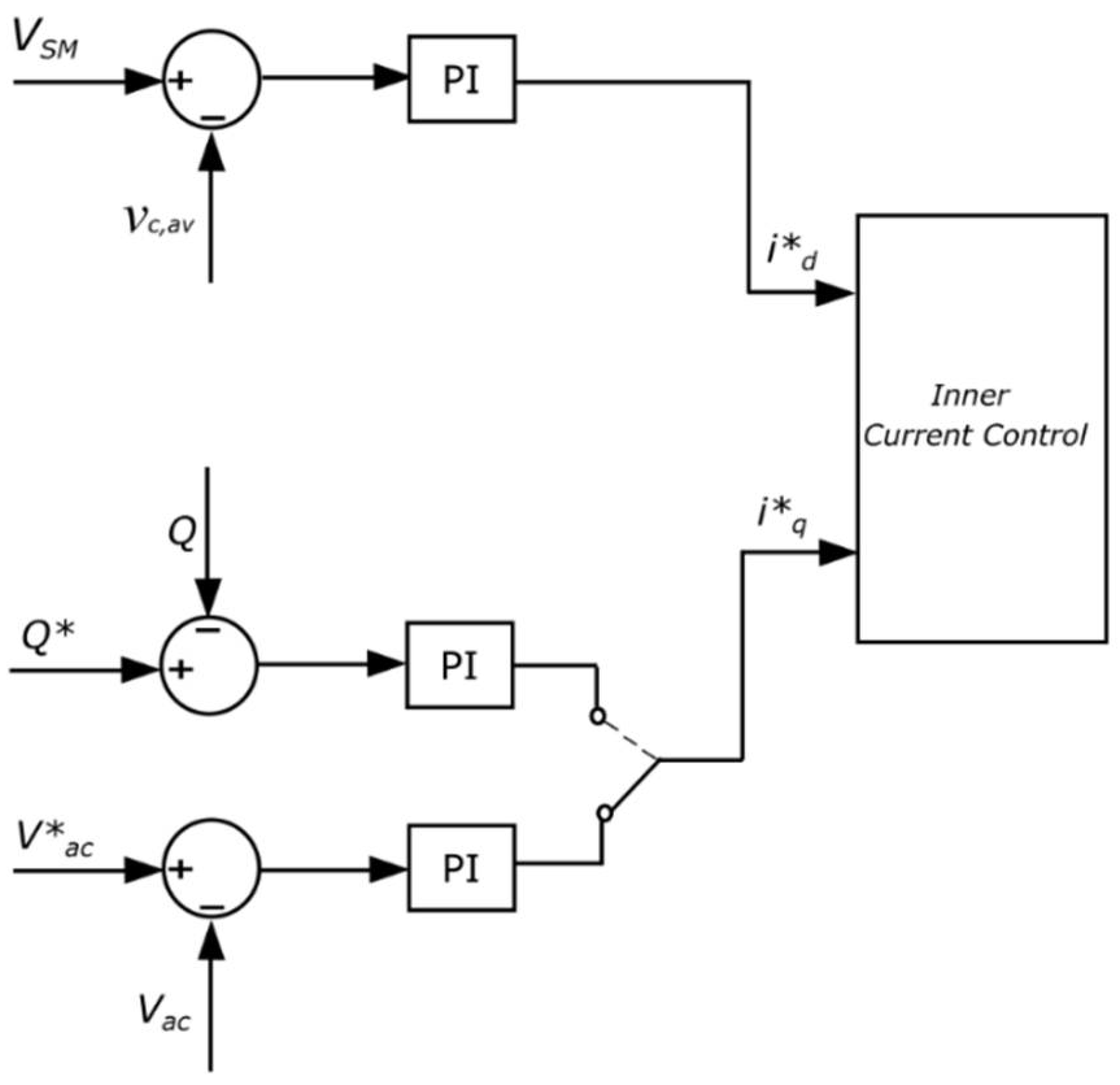
Another essential change in the MMC control to maintain energy balance when operating as a STATCOM during the fault is in the outer controllers as suggested by the authors in [38], more specifically in the P / V D C loop that provides the reference for the d-axis current. When a DC fault occurs, active power cannot be transferred through the DC line. Therefore, the active power reference should be set to zero. However, some active power will need to be provided to the SMs to account for the losses in the switches. Therefore, the d-axis current reference should be provided by some other means than P / V D C . This change is illustrated in Figure 5, where the d-axis current reference is obtained through a PI controller involving V S M , the nominal SM capacitor voltage, and v c , a v , the average value of the measured capacitor voltages of all SMs in the MMC.
Such an outer loop would ensure that the average capacitor voltage, and therefore the total energy stored in the MMC capacitors, is kept reasonably constant during the fault. The conventional sorting algorithm [30] is kept in place to ensure equal voltage distribution in all six MMC arms. The control diagram for all three modes of operation is shown in Figure 6.

4. Proposed Control Scheme to Enable Fast DC Fault Current Suppression

It has already been established that activating reverse discharge control after detection of DC fault will force the DC fault current to change direction and have a zero-crossing. However, the fault current will continue to increase in the reverse direction after the zero-crossing if no further action is taken. Therefore, the arm voltage references must be modified so that they synthesize zero volts at the DC poles thereby clearing the fault. The MMC(s) can then be operated as STATCOM(s) to provide AC side voltage support. The benefit of utilizing reverse discharge control after fault detection is that it would bring about a rapid zero-crossing following which the fault can be cleared and the switch to the STATCOM operation can be made. Clearing the fault and initiating STATCOM operation at lower values of the DC fault current leads to lower oscillations and, by extension, faster fault current suppression. The flow chart for the proposed control scheme to provide fast fault current suppression during DC-FRT and reactive power support to the AC grid is shown in Figure 7. In the next section, the proposed scheme is verified through simulations in a point-to-point HVDC connection. Reverse SM discharge is based on local current measurements and can bring about a zero-crossing in any MMC terminal contributing to the DC fault. Therefore, the proposed scheme can be used in multi-terminal HVDC systems as well.

5. Simulation Results

In this section, first, the test system is described and then the performance of the proposed control scheme is verified through various simulation studies in the PSCAD/EMTDC environment. The simulation results are mainly provided for terminal 2, while similar observations and conclusions can be made about terminal 1.

5.1. Test System

The test system consists of a point-to-point HVDC connection, with FBSM-based MMCs at either end, as shown in Figure 8. The relevant parameters are given in Table 1 and Table 2.
The parameters of the equivalent circuit corresponding to the test system are:
L e = 2 L s 3 + L D C = 83.33   mH ,
R e = 2 R s 3 + R f = 1   Ω ,
C e = 3 C d 2 N = 59.21   μ F .
Table 3 shows D 2 values to ensure critical damping for different values of the fault resistance and the inductance of the DC line reactor. As an example, if the test system fault resistance is 1 Ω and the DC line reactor’s inductance is 50 mH, then any value of D 2 selected over 0.013 will ensure an underdamped fault circuit.
The selection of D 2 can be made according to inductor specifications since a high di/dt can cause an overvoltage in the inductors. If the inductors have an upper voltage limit, then D 2 can be used to meet specific di/dt targets.
In the test system, the MMCs are controlled by the conventional dq method described earlier. The circulating current suppression controller described in [35] is implemented as well. MMC 1 controls the active power while MMC 2 controls the DC voltage. The DC line voltage is 640 kV and transfers 900 MW of power, which results in a DC current of 1.5 kA. The fixed power load draws an active power of 150 MW and reactive power of 150 MVAr per phase. A permanent pole-to-pole fault is applied in the middle of the 300 km-long DC line at t = 3 s, with a fault resistance of 1 Ω. As soon as the fault occurs, the fault current increases rapidly due to the discharge of FBSM capacitors. The fault detection delay is assumed to be 2 ms. After the fault is detected, both converters are put into D 2 reverse discharge control mode. When the measurement of the DC line current at the corresponding terminal reaches zero, the fault is cleared by adjusting the arm voltage references and STATCOM operation is initiated to provide AC side voltage support. The outer control loops making the d-axis current references in both MMCs are switched to V S M control to ensure energy balance.

5.2. DC Fault Current Suppression

Figure 9 shows the DC currents at both terminals after the occurrence of a pole-to-pole DC fault and subsequent reverse discharge control initiation for different D 2 values. The waveforms clearly show that initiating controlled reverse discharge of the SMs impacts the rate of fall of the DC fault current, with higher values of D 2 resulting in faster zero-crossings for both i D C 1 and i D C 2 .
The next step is to check the viability of the proposed control method where the reverse SM discharge control is followed by DC fault clearance and subsequent switch to the STATCOM operation mode after the DC current zero-crossing at the respective MMCs. The value of D 2 is varied between 0.125 and 0.5 and the DC currents measured at both MMCs are plotted in Figure 10. DC current values for cases when the MMCs are blocked, bypassed and when STATCOM operation is initiated immediately upon fault detection are added to the plots to provide an effective comparison between the proposed control scheme and conventional FRT methods.
The results show that blocking the MMCs is the fastest way to suppress the fault currents while the bypass mode is the slowest. Furthermore, Figure 10 shows that higher values of D 2 result in higher DC fault current falling slopes. Therefore, reverse discharge control with higher values of D 2 causes the DC current to cross zero in a shorter timeframe. Once the zero-crossing is reached, the DC fault is cleared by adjusting the arm voltage references and initiating the STATCOM operation. Due to the fault being cleared at lower values of the DC current, the proposed control scheme is seen to be significantly superior in terms of fault current suppression time when compared to the conventional FRT method, in which the converter is immediately operated as a STATCOM upon detection of the fault. The proposed scheme with D 2 = 0.125 can bring the DC fault current at both terminals under 1 p.u. (1.56 kA on transformer high-voltage side) within 0.005 s, while this takes around 0.05 s using the conventional method (STATCOM in the plots). Meanwhile, the blocking method suppresses the fault current in 0.004 s, which is comparable to the suppression times obtained through the proposed scheme.

5.3. AC Side Currents

Figure 11 shows the AC side currents for terminal 2. The blocking mode can suppress the fault current through the MMC very quickly, resulting in smooth AC side currents at terminal 2, although this mode cannot provide voltage support to the AC grid. As expected, the bypass mode ( D 2   = 0) results in very high AC side currents. This is because when the SMs are bypassed, the DC side fault is transformed into an AC side short circuit leading to drops in the DC and hence the AC side voltages at the terminal. Lower D 2 values imply a higher proportion of SMs are bypassed, thus resulting in higher transient peaks in the AC side currents. No noticeable differences are observed in the AC side current waveforms between the conventional operation of the converter as a STATCOM upon fault detection and the proposed scheme utilizing high values of D 2 .
Figure 12a shows the phase a voltage and current waveforms at Terminal 2. It can be observed that the phase angle between the current and voltage is approximately 21° during normal operation and 90° after fault detection. This implies the post-fault operation of the MMC as a STATCOM. In Figure 12b, the magnitudes of the fundamental component, as well as the second and third harmonics of phase a current measured at Terminal 2, are shown. Figure 12b shows that the proposed scheme does not increase the harmonic contents of the current.

5.4. Arm Currents

Figure 13 shows the currents in all six arms of MMC 2. Blocking the IGBTs results in very fast suppression of the MMC arm currents. Meanwhile, the bypass mode results in the highest arm current amplitudes. This is to be expected since bypassing the SMs converts the DC side short circuit to an AC side short circuit. These high AC side currents do not flow into the DC fault; instead, they circulate within the arms of the converter. The proposed scheme is seen to keep better control over the arm current transient peaks compared to conventional DC fault clearance/STATCOM operation mode, provided high D 2 values are utilized. This is a direct consequence of reduced oscillations in the DC side current since approximately one-third of the DC current flows through each leg of the MMC. It should be noted that lower D 2 values will lead to higher transient fluctuations in the arm currents and, therefore, IGBT ratings must be taken into account when the selection is made.

5.5. Terminal Voltage

Figure 14 shows the RMS value of the line-line voltage at terminal 2 before and after DC side fault occurrence. In blocking mode, terminal 2 voltage shows a significant drop to about 200 kV. This is because there is a fixed load connected to it that draws a constant power of 150 MW and 150 MVAr per phase. MMC 2 being blocked cannot provide reactive power support to the AC grid, causing a drop in terminal 2 voltage. In bypass mode, the DC side fault transforms into an AC side short circuit leading to a significant voltage drop at the terminal to about 75 kV. As for the performance of the proposed scheme with high D 2 values, the results are similar to the conventional DC fault clearance/STATCOM operation mode. Lower D 2 values result in greater fluctuations due to higher voltage drop at the terminal during reverse discharge control.

5.6. Capacitor Voltages

Figure 15 shows the sum of the capacitor voltages ( S x u and S x l where x = a , b , c ) for all arms of MMC 2. In the blocking mode, there is no current flow through the MMC arms and the SM capacitor voltages remain constant throughout the fault. The outcome is similar to the bypass mode in which the arm currents do not flow through the SM capacitors. The results also indicate that in the proposed control scheme, the modified V S M control, along with the conventional sorting method, keeps the arm energies very well balanced. The proposed control scheme maintains arm energy balance better than the conventional DC fault clearance/STATCOM mode of operation during the transient period provided that high D 2 values are utilized. This is because in the conventional method, the arm current transient peaks are higher, leading to greater fluctuations in the capacitor voltages.

6. Conclusions

This paper presents a control scheme suitable for fast DC fault current suppression in full-bridge modular multi-level converters (FB-MMCs). The goal behind the proposed scheme was to provide a simple method for fault-tolerant MMC systems to facilitate fast DC fault current suppression, as well as providing AC side voltage support while riding through DC faults. The regulation of SM capacitor discharge was performed in the reverse direction, facilitating a fast drop-off of the DC fault current towards zero-crossing and an immediate reversal in the fault current direction. DC fault clearance by the adjustment of arm voltage references and STATCOM operation was initiated in the MMCs immediately after zero-crossing of the DC fault current was detected. Extensive simulation studies verified the performance of the proposed control method and demonstrated how it reduced oscillations leading to significantly faster fault current suppression when compared to existing DC FRT methods. Furthermore, with the proposed control scheme, MMC arm currents were kept under control more effectively during DC fault transients compared to the conventional method of clearing the DC fault and initiating STATCOM operation immediately upon fault detection. Consequently, fluctuations in the capacitor voltages were reduced during fault transients, leading to better overall DC-FRT performance. Utilization of high values of the insertion parameter in the proposed scheme was seen to be beneficial in almost all aspects such as low AC side and MMC arm current transient peaks, resulting in a better SM capacitor voltage balancing performance and lower peak current rating requirement for the IGBTs. The only drawback of utilizing high values of the insertion parameter in the proposed scheme lies in the possibility of causing overvoltage in the MMC arm inductors.

Author Contributions

Conceptualization, M.N.S., S.P.A. and M.K.; methodology, M.N.S.; software, M.N.S.; validation, S.P.A. and M.K.; formal analysis, M.N.S.; investigation, M.N.S.; resources, S.P.A. and M.K.; data curation, M.N.S.; writing—original draft preparation, M.N.S.; writing—review and editing, S.P.A. and M.K.; visualization, M.N.S.; supervision, S.P.A. and M.K.; project administration, S.P.A. and M.K. All authors have read and agreed to the published version of the manuscript.

Funding

This research was funded by a Discovery Grant provided by the Natural Sciences and Engineering Research Council (NSERC) of Canada and an Ontario Graduate Scholarship (OGS) provided by the provincial Government of Ontario, Canada.

Institutional Review Board Statement

Not applicable.

Informed Consent Statement

Not applicable.

Data Availability Statement

The data utilized in this study are available within the article.

Conflicts of Interest

The authors declare no conflict of interest.

References

  1. Halder, T. Comparative study of HVDC and HVAC for a bulk power transmission. In Proceedings of the 2013 International Conference on Power, Energy and Control (ICPEC), Dindigul, India, 6–8 February 2013; pp. 139–144. [Google Scholar]
  2. Oni Davidson, I.; Mbangula, K. A review of LCC-HVDC and VSC-HVDC technologies and applications. In Proceedings of the IEEE 16th International Conference on Environment and Electrical Engineering (EEEIC), Florence, Italy, 7–10 June 2016; pp. 1–7. [Google Scholar]
  3. Lesnicar, A.; Marquardt, R. An innovative modular multilevel converter topology suitable for a wide power range. In Proceedings of the 2003 IEEE Bologna Power Tech Conference Proceedings, Bologna, Italy, 23–26 June 2003. [Google Scholar]
  4. Wang, S.; Li, C.; Adeuyi, O.D.; Li, G.; Ugalde-Loo, C.E.; Liang, J. Coordination of MMCs With Hybrid DC Circuit Breakers for HVDC Grid Protection. IEEE Trans. Power Deliv. 2019, 34, 11–22. [Google Scholar] [CrossRef] [Green Version]
  5. Song, S.-M.; Kim, J.-Y.; Choi, S.-S.; Kim, I.-D.; Choi, S.-K. New Simple-Structured AC Solid-State Circuit Breaker. IEEE Trans. Ind. Electron. 2018, 65, 8455–8463. [Google Scholar] [CrossRef]
  6. Nami, A.; Liang, J.; Dijkhuizen, F.; Demetriades, G. Modular Multilevel Con-verters for HVDC Applications: Review on Converter Cells and Functionalities. IEEE Trans. Power Electron. 2015, 30, 18–36. [Google Scholar] [CrossRef]
  7. Nguyen, T.H.; Hosani, K.A.; Moursi, M.S.E.; Blaabjerg, F. An Overview of Modular Multilevel Converters in HVDC Transmission Systems with STATCOM Operation During Pole-to-Pole DC Short Circuits. IEEE Trans. Power Electron. 2019, 34, 4137–4160. [Google Scholar] [CrossRef]
  8. Wang, Y.; Yuan, Z.; Fu, J.; Li, Y.; Zhao, Y. A feasible coordination protection strategy for MMC-MTDC systems under DC faults. Int. J. Electr. Power Energy Syst. 2017, 90, 103–111. [Google Scholar] [CrossRef]
  9. Li, B.; He, J.; Tian, J.; Feng, Y.; Dong, Y. DC fault analysis for modular multilevel converter-based system. J. Mod. Power Syst. Clean Energy 2017, 5, 275–282. [Google Scholar] [CrossRef] [Green Version]
  10. Kontos, E.; Tsolaridis, G.; Teodorescu, R.; Bauer, P. On DC Fault Dynamics of MMC-Based HVdc Connections. IEEE Trans. Power Deliv. 2018, 33, 497–507. [Google Scholar] [CrossRef]
  11. Cwikowski, O.; Wickramasinghe, H.; Konstantinou, G.; Pou, J.; Barnes, M.; Shuttleworth, R. Modular Multilevel Converter DC Fault Protection. IEEE Trans. Power Deliv. 2018, 33, 291–300. [Google Scholar] [CrossRef] [Green Version]
  12. Li, X.; Song, Q.; Liu, W.; Rao, H.; Xu, S.; Li, L. Protection of Nonpermanent Faults on DC Overhead Lines in MMC-Based HVDC Systems. IEEE Trans. Power Deliv. 2013, 28, 483–490. [Google Scholar] [CrossRef]
  13. Ni, B.; Xiang, W.; Zhou, M.; Zuo, W.; Yao, W.; Lin, W.; Wen, J. An Adaptive Fault Current Limiting Control for MMC and Its Application in DC Grid. IEEE Trans. Power Deliv. 2021, 36, 920–931. [Google Scholar] [CrossRef]
  14. Li, X.; Li, Z.; Zhao, B.; Lu, C.; Song, Q.; Zhou, Y.; Rao, H.; Xu, S.; Zhu, Z. HVdc Reactor Reduction Method Based on Virtual Reactor Fault Current Limiting Control of MMC. IEEE Trans. Ind. Electron. 2020, 67, 9991–10000. [Google Scholar] [CrossRef]
  15. Qin, J.; Saeedifard, M.; Rockhill, A.; Zhou, R. Hybrid Design of Modular Multi-level Converters for HVDC Systems Based on Various Submodule Circuits. IEEE Trans. Power Deliv. 2015, 30, 385–394. [Google Scholar] [CrossRef]
  16. Li, R.; Fletcher, J.; Xu, L.; Holliday, D.; Williams, B. A Hybrid Modular Multilevel Converter with Novel Three-Level Cells for DC Fault Blocking Capability. IEEE Trans. Power Deliv. 2015, 30, 2017–2026. [Google Scholar] [CrossRef] [Green Version]
  17. Nami, A.; Wang, L.; Dijkhuizen, F.; Shukla, A. Five level cross connected cell for cascaded converters. In Proceedings of the 2013 15th European Conference on Power Electronics and Applications (EPE), Lille, France, 2–6 September 2013. [Google Scholar]
  18. Ilves, K.; Bessegato, L.; Harnefors, L.; Norrga, S.; Nee, H.-P. Semi-full-bridge submodule for modular multi-level converters. In Proceedings of the 2015 9th International Conference on Power Electronics and ECCE Asia (ICPE-ECCE Asia), Seoul, Korea, 1–5 June 2015. [Google Scholar]
  19. Sakib, M.; Azad, S.; Kazerani, M. A Critical Review of Modular Multilevel Converter Configurations and Submodule Topologies from DC Fault Blocking and Ride-Through Capabilities Viewpoints for HVDC Applications. Energies 2022, 15, 4176. [Google Scholar] [CrossRef]
  20. Debnath, S.; Qin, J.; Bahrani, B.; Saeedifard, M.; Barbosa, P. Operation, control, and applications of the modular multilevel converter: A Review. IEEE Trans. Power Electron. 2015, 30, 37–53. [Google Scholar] [CrossRef]
  21. Cui, S.; Sul, S.-K. A Comprehensive DC Short-Circuit Fault Ride through Strategy of Hybrid Modular Multilevel Converters (MMCs) for Overhead Line Transmission. IEEE Trans. Power Electron. 2016, 31, 7780–7796. [Google Scholar] [CrossRef]
  22. Shahriari, E.; Gruson, F.; Vermeersch, P.; Delarue, P.; Colas, F.; Guillaud, X. A Novel DC Fault Ride through Control Methodology for Hybrid Modular Multilevel Converters in HVDC Systems. IEEE Trans. Power Deliv. 2020, 35, 2831–2840. [Google Scholar] [CrossRef]
  23. Xiang, W.; Lin, W.; Xu, L.; Wen, J. Enhanced Independent Pole Control of Hybrid MMC-HVdc System. IEEE Trans. Power Deliv. 2018, 33, 861–872. [Google Scholar] [CrossRef] [Green Version]
  24. Li, X.; Zhao, B.; Wei, Y.; Xie, X.; Hu, Y.; Shu, D. DC fault current limiting effect of MMC submodule capacitors. Int. J. Electr. Power Energy Syst. 2020, 115, 105444. [Google Scholar] [CrossRef]
  25. Hagiwara, M.; Akagi, H. Control and Experiment of Pulsewidth-Modulated Modular Multilevel Converters. IEEE Trans. Power Electron. 2009, 24, 1737–1746. [Google Scholar] [CrossRef]
  26. Durrant, M.; Werner, H.H.; Abbott, K. Modelling and controller design for VSC-HVDC attached to an AC network. In Proceedings of the European Control Conference (ECC), Cambridge, UK, 1–4 September 2003. [Google Scholar]
  27. Meshram, P.M.; Borghate, V.B. A Simplified Nearest Level Control (NLC) Voltage Balancing Method for Modular Multilevel Converter (MMC). IEEE Trans. Power Electron. 2015, 30, 450–462. [Google Scholar] [CrossRef]
  28. Konstantinou, G.S.; Ciobotaru, M.; Agelidis, V.G. Analysis of multi-carrier PWM methods for back-to-back HVDC systems based on modular multilevel converters. In Proceedings of the IECON 2011—37th Annual Conference of the IEEE Industrial Electronics Society, Melbourne, Australia, 7–10 November 2011. [Google Scholar]
  29. Lizana, R.F.; Pérez, M.A.; Rodríguez, J. DC voltage balance control in a modular multilevel cascaded converter. In Proceedings of the IEEE International Symposium on Industrial Electronics (ISIE), Hangzhou, China, 28–31 May 2012. [Google Scholar]
  30. Saeedifard, M.; Iravani, R. Dynamic Performance of a Modular Multilevel Back-to-Back HVDC System. IEEE Trans. Power Deliv. 2010, 25, 2903–2912. [Google Scholar] [CrossRef]
  31. Nguyen, M.; Kwak, S.; Kim, T. Phase-Shifted Carrier Pulse-Width Modulation Algorithm with Improved Dynamic Performance for Modular Multilevel Converters. IEEE Access 2019, 7, 170949–170960. [Google Scholar] [CrossRef]
  32. Ronanki, D.; Williamson, S.S. Modified Phase-disposition PWM Technique for Modular Multilevel Converters. In Proceedings of the 2018 IEEE Transportation Electrification Conference and Expo (ITEC), Long Beach, CA, USA, 13–15 June 2018. [Google Scholar]
  33. Deng, Y.; Saeedifard, M.; Harley, R.G. An improved nearest-level modulation method for the modular multilevel converter. In Proceedings of the 2015 IEEE Applied Power Electronics Conference and Exposition (APEC), Charlotte, NC, USA, 15–19 March 2015; pp. 1595–1600. [Google Scholar] [CrossRef]
  34. Moon, J.-W.; Kim, C.-S.; Park, J.-W.; Kang, D.-W.; Kim, J.-M. Circulating Current Control in MMC under the Unbalanced Voltage. IEEE Trans. Power Deliv. 2013, 28, 1952–1959. [Google Scholar] [CrossRef]
  35. Guide for the Development of Models for HVDC Converters in a HVDC Grid; B4.57 CIGRE Brochure 604 (Working Group); CIGRE: Paris, France, 2014.
  36. Wang, K.; Li, Y.Y.; Zheng, Z.; Xu, L. Voltage Balancing and Fluctua-tion-Suppression Methods of Floating Capacitors in a New Modular Multilevel Converter. IEEE Trans. Ind. Electron. 2013, 60, 1943–1954. [Google Scholar] [CrossRef]
  37. Cui, S.; Kim, S.; Jung, J.-J.; Sul, S.-K. Principle, control and comparison of modular multilevel converters (MMCs) with DC short circuit fault ride-through capabil-ity. In Proceedings of the 2014 IEEE Applied Power Electronics Conference and Exposition—APEC 2014, Fort Worth, TX, USA, 6–20 March 2014. [Google Scholar]
  38. Kontos, E.; Tsolaridis, G.; Teodorescu, R.; Bauer, P. Full-bridge MMC DC fault ride-through and STATCOM operation in multi-terminal HVDC grids. Bull. Pol. Acad. Sci. Tech. Sci. 2017, 65, 653–662. [Google Scholar] [CrossRef] [Green Version]
  39. Gao, S.; Ye, H.; Liu, Y. Accurate and Efficient Estimation of Short-Circuit Current for MTDC Grids Considering MMC Control. IEEE Trans. Power Deliv. 2020, 35, 1541–1552. [Google Scholar] [CrossRef]
Figure 1. (a) Structure of a three-phase MMC; (b) the Half-Bridge SM (HBSM); (c) the Full-Bridge SM (FBSM).
Energies 15 04595 g001
Figure 2. MMC control.
Energies 15 04595 g002
Figure 3. Equivalent circuits for SM capacitor discharge control: (a) Base Circuit 1; (b) Base Circuit 2; and (c) Base Circuit 3.
Energies 15 04595 g003
Figure 4. Arm voltage references for (a) conventional discharge control using D 1 ; (b) reverse discharge control using D 2 ; (c) DC fault clearance and STATCOM operation.
Energies 15 04595 g004
Figure 5. Outer controllers during STATCOM operation.
Energies 15 04595 g005
Figure 6. Control diagram.
Energies 15 04595 g006
Figure 7. Flowchart for the proposed control scheme.
Energies 15 04595 g007
Figure 8. Test System.
Energies 15 04595 g008
Figure 9. DC currents at the terminals during reverse discharge control mode.
Energies 15 04595 g009
Figure 10. DC currents during reverse discharge control scheme and conventional FRT methods: (a) Terminal 1; (b) Terminal 2.
Energies 15 04595 g010
Figure 11. AC side currents at Terminal 2.
Energies 15 04595 g011
Figure 12. (a) Waveforms of the phase a current injected by MMC 2 into Terminal 2 and the voltage at Terminal 2; (b) Magnitude of fundamental component, and the second and third harmonics of phase a current at Terminal 2.
Energies 15 04595 g012
Figure 13. Arm currents of MMC 2.
Energies 15 04595 g013
Figure 14. Line-to-line RMS voltage at Terminal 2.
Energies 15 04595 g014
Figure 15. Sum of capacitor voltages in all six arms of MMC 2.
Energies 15 04595 g015
Table 1. Test System Parameters.
ParametersMMC 1MMC 2
Operating Condition−900 MW
(Active Power Control)
640 kV
(DC Voltage Control)
Capacity (Prated)1000 MW1000 MW
SM Capacitance (C)3 mF3 mF
Carrier Frequency (fc)300 Hz300 Hz
Number of SMs per arm (N)7676
IGBT and Diode On-State Resistance (Rd)0.005 Ω 0.005 Ω
Arm Inductance (Ls)50 mH50 mH
Arm Resistance (Rs)0 Ω0 Ω
DC Line Reactor Inductance (LDC)50 mH50 mH
Nominal AC Voltage (Vac,LL)240 kV230 kV
Transformer Reactance (Xt)0.1 pu0.1 pu
Transformers230 kV: 370 kV230 kV: 370 kV
Table 2. HVDC Transmission Line Parameters [39].
ItemValue
Resistance per unit length0.009735 Ω/km
Inductance per unit length0.0176 mH/km
Capacitance per unit length0.001367 µF/km
Table 3. Critical values of D2 with variation in Rf and LDC.
Rf (Ω)LDC (mH)Critical D2
1500.013
11000.009
12000.0067
10500.13
101000.094
102000.067
Publisher’s Note: MDPI stays neutral with regard to jurisdictional claims in published maps and institutional affiliations.

