Abstract
In this paper, a voltage-boost-type non-voltage drop single-phase full-bridge inverter connected to a switched-capacitor structure is proposed. The output voltage of the inverter is controlled by the pulse width modulation of a DSP to control the lead and break of the active switches. The full-bridge switches work at low frequency; the other switches work at high frequency. The inverter uses two capacitor modules to charge and discharge alternately so as to overcome the problem of voltage drop on the output side of the inverter in the transition stage from series capacitor discharge to parallel charge. By analyzing the charge–discharge characteristics of the RC charge–discharge circuit, the capacitor charge–discharge cycle can be adjusted to alter the output voltage within a certain range. The results from the physical construction verify the Simulation results achieved well, which demonstrates satisfactory performance that supports the verification of the above theory.
1. Introduction
Fossil fuels are the world’s main resource for energy production [1,2], with the use of coal, oil, and natural gas underpinning the progress of human civilization and its economic and social development since the 19th century. The use of fossil fuel energy generates huge amounts of gases, such as CO2, which intensify the greenhouse effect, causing thermal pollution and threatening the global ecology. It has therefore become even more pressing to seek abundant, clean, and pollution-free renewable energy sources, with photovoltaic power generation, wind power generation, and tidal power generation becoming the mainstream in alternative clean energy sources widely adopted and valued by society [3,4,5].
In the renewable energy utilization system, the power electronic inverter is the key link between electric energy conversion and transmission [6]. With the development of power and electronic technologies, the industry has been putting an increasing demand on the efficiency of the inverter system and the characteristics of the output voltage waveform [7,8]. However, traditional inverter-based distributed power generation has a flaw in its application. Its output side voltage is always lower than the input side voltage value, which cannot meet the requirements of the voltage level at the DC side of the grid-connected inverter. As a result, it is impossible to directly use distributed electric energy to supply power to the load [9,10,11].
In order to solve this problem, the common practice is to use many traditional boost converters. However, in practical applications, their boosting capacity is limited. If the boosting capacity needs to be continuously improved, the duty cycle must be increased, which brings problems such as increased stress on the diode voltage and current [12,13,14,15]. The authors of [16,17,18] propose a Z-source inverter, which realizes the boost of the inverter by changing the through duty cycle, resulting in a good waveform of the inverter output current. However, the Z-source inverter has disadvantages, such as large starting current impact, and comes with large volume. In addition, high-gain boost converters can be classified into two categories: isolated and non-isolated. In comparison to isolated converters, non-isolated converters demonstrate many advantages, such as simple structure, small size, and high efficiency [19], but changes in their common-mode voltage will bring conduction losses [20]. Coupled inductor usage can also increase the boost ratio of the converter, but the efficiency is low and the circuit is complicated. The active clamp flyback converter can suppress the voltage spike of the switching tube, but the input current of the converter is intermittent, and the pulsation is large [21,22,23]. In the isolation transformer, the transformer plays a role in voltage matching, and electrical isolation improves the safety of the system. However, the transformer increases the volume and cost of the entire system and reduces its efficiency [24]. Relevant scholars proposed multi-phase inverters [25,26], which increase the output power by paralleling the outputs of multiple inverters. However, the circulating current caused by the parameter difference between the inverters needs to be eliminated.
In order to overcome the shortcomings of the traditional inverter structure and reduce the number of components and control complexity of the system, switched-capacitor technology has been applied to the multi-level inverter structure in recent years [27,28,29,30]. This structure can convert non-adjustable voltage direct current into adjustable voltage direct current [31,32]. The authors of [33] combined multiple switched-capacitor modules in series and parallel and increased the gain of the converter by increasing the number of input terminals. The authors of [34] proposed a design method that combines switched capacitors with coupled inductance technology. This scheme integrates boost circuit and fly-back circuit, connecting their output sides in series, with the converter obtaining a higher boost multiple.
However, when domestic and foreign scholars chose a switched-capacitor converter to boost the voltage, there was an output side voltage drop caused by the parallel charging of capacitors, and this has not been effectively resolved.
Therefore, this paper proposes that the switched-capacitor structure can bring about a significant voltage boost effect. Two capacitor modules with the same structure and different pulse sequences can be used to control their alternating charging and discharging, which helps overcome the problem of voltage drop on the output side of the converter during the stage of capacitor series discharge to parallel charging. By adjusting the charge and discharge cycle of the capacitor, the output side voltage can be independently adjusted within a certain range. Compared with other inverters, the proposed inverter has the advantages of simple modulation strategy, strong flexibility, small power switching voltage stress, and high conversion efficiency. Two symmetrical capacitor charging and discharging modules solve the problem of inverter output voltage sag during capacitor charging.
2. Circuit Structure and Working Principle
2.1. Circuit Structure
The topology of the new converter is shown in Figure 1. The inverter includes a full-bridge inverter module, the first capacitor module, the second capacitor module, and a DC input power supply Vin; the full-bridge inverter module is managed by MOSFET S1, S2, S3, S4, and load resistor R1; the first capacitor module is composed of resistor R1, capacitor C1, MOSFET S5, S6, S9, and DC input power Vin; the second capacitor module is composed of resistor R3, capacitor C2, MOSFET S7, S8, S11, and DC input power Vin.
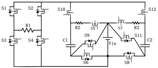
Figure 1.
Circuit structure.
Turning on S5 and S6, S7 and S8 simultaneously, the resistor and the capacitor are energized in series, and C1 and C2 are charged in parallel through the DC input power supply, where the resistance is the current limiting resistor; turning off S5 and S6, S7 and S8, and meanwhile, turning on S9 and S10, S11 and S12, the capacitors C1 and C2 are, respectively, discharged in series with the DC input power supply.
When the inverter starts to work, in the first stage, C1 and C2 are charged at the same time. In the remaining stages, S10 and S9 of the first capacitor module are turned on and off synchronously, S12 and S11 of the second capacitor module are turned on and off synchronously, and S12 and S11 are opposite to S10 and S9. Similarly, S5 and S6 of the first capacitor module are turned on and off synchronously, S7 and S8 of the second capacitor module are turned on and off synchronously, and S5 and S6 are opposite to S7 and S8. In a power frequency cycle, the two capacitor modules work alternately under high frequency conditions.
2.2. Working Principle
This article defines the direction of current flowing through the MOS tube as D (drain) into S (source). From the circuit structure diagram of Figure 1, it can be seen that except for MOSFET S10, S12, S5, and S7, the other MOS tubes are all anti-parallel diodes. The reason is that these four MOS tubes must meet the forward conduction and reverse cut-off conditions. If the diodes are in reverse parallel, current loops will appear, which will affect the charging and discharging process of the capacitor and change the output voltage. Figure 2 shows the situation in which four MOS tubes can be replaced during the actual implementation (a special case).
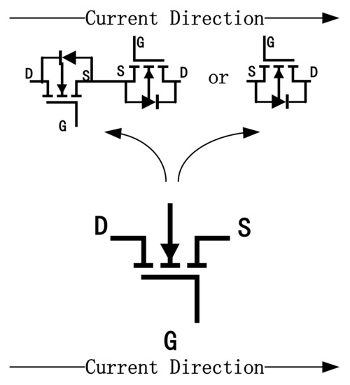
Figure 2.
The specific circumstances under which the MOS tube can be replaced.
If MOSFET S10, S12, S5, and S7 are anti-parallel diodes, this article takes a pair of bridge arms as an example, and the circuit situation that appears is shown in Figure 3 and Figure 4.
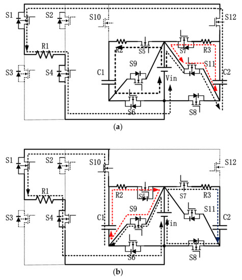
Figure 3.
Disallowed working current path: (a) S7 anti-parallel diode case; (b) S5 anti-parallel diode case.
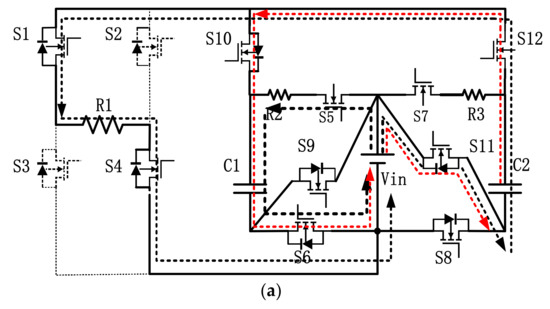
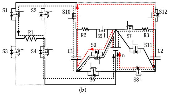
Figure 4.
Disallowed working current path: (a) S10 anti-parallel diode case; (b) S12 anti-parallel diode case.
The black current loop is the normal working loop, and the red loop is the unnecessary loop formed when the MOS tube is inversely parallel with the diode.
The situation of S7 and S5 is similar. For example, the situation of S7 anti-parallel diode can be explained as follows:
The VGS (gate-source) voltage of S7 is removed. At this time, the capacitor C2, resistor R3, S11 and the anti-parallel diode of S7 form a new working circuit. In the current state, the fully charged capacitor C2 is discharged in series with the DC input power supply. C2 itself is equivalent to a power supply, and the resistor R3 is connected in series, so the average voltage at the output side of the inverter is lower than normal. The current path of this working state is shown in Figure 3a,b.
The situation of S10 and S12 is similar. For example, the situation of S10 anti-parallel diode can be explained as follows:
The VGS (gate-source) voltage of S10 is removed. At this time, the DC input power supply Vin, capacitor C2, capacitor C1, S11, S12, and S6 form a new working circuit through the anti-parallel diode of S10. In the current state, the average voltage of capacitor C1 rises compared to normal, the voltage formed by the series connection of the DC source Vin and the capacitor C2 is divided, and the average voltage at the output side of the inverter decreases. The current path of this working state is shown in Figure 4a,b.
Under normal circumstances, the proposed topology has five different operating modes:
First mode: This mode occurs before the full-bridge switching action. In this mode, S5 and S6 of the first capacitor module and S7 and S8 of the second capacitor module are turned on at the same time, and the remaining MOS tubes are all turned off. At this time, capacitors C1 and C2 are charged in series with R2 and R3 through the DC input power supply. The current path of this specific working state is shown in Figure 5.
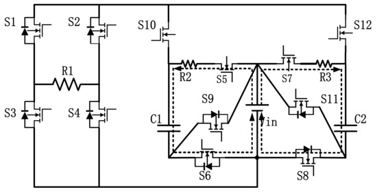
Figure 5.
First-mode working current path.
Second mode: Full bridge 1, four bridge arms are active; S1 and S4 work at 50 Hz; S2 and S3 are turned off. In the first half of the cycle, the first capacitor module and the second capacitor module alternately charge and discharge at a high frequency.
In this mode, when the first capacitor module is charged and the second capacitor module is discharged, S9 and S10 are turned off; S5 and S6 are turned on. When S11 and S12 are turned on, S7 and S8 are turned off. Capacitor C1 remains charged, and the fully charged capacitor C2 is discharged in series with the DC input power supply. The current path of this working state is shown in Figure 6a.
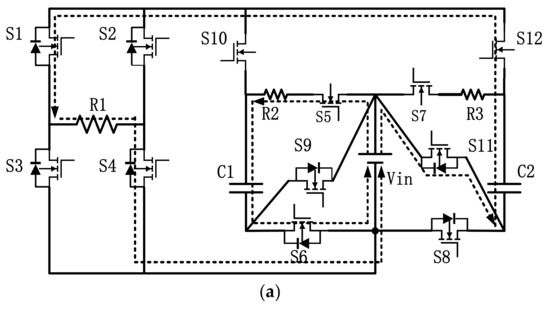
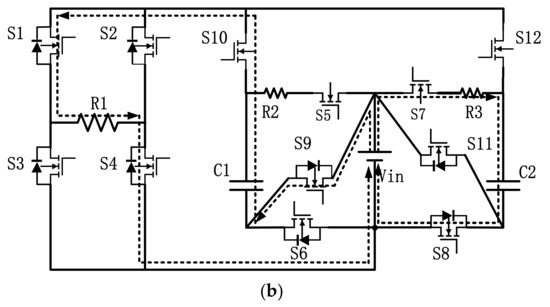
Figure 6.
Full bridge 1, 4 bridge arms are active; working current path: (a) second-mode working current path; (b) third-mode working current path.
Third mode: Full bridge 1, four bridge arms are active; S1 and S4 work at 50 Hz; S2 and S3 are turned off. In the first half of the cycle, the first capacitor module and the second capacitor module are alternately charging and discharging at a high frequency.
In this mode, when the first capacitor module is discharged and the second capacitor module is charged, S9 and S10 are turned on; S5 and S6 are turned off. When S11 and S12 are turned off, S7 and S8 are turned on, the capacitor C2 enters the charging state, and at this time, the capacitor C1 is discharged in series with the DC input power supply. The current path of this working state is shown in Figure 6b.
Fourth mode: S2 and S3 work at a power frequency 50 Hz; S1 and S4 are turned off. In the second half of the cycle, similar to the second mode, the first capacitor module is charged, and the second capacitor module is discharged. Pulse width modulation is performed by the DSP to control the MOS tubes to turn on and off; C1 enters the charging state; and the fully charged capacitor C2 is discharged in series with the DC input power supply. The current path of this working state is shown in Figure 7a.
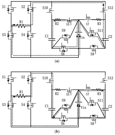
Figure 7.
Full bridge 2, 3 bridge arms are active; working current path: (a) fourth-mode working current path; (b) fifth-mode working current path.
Fifth mode: S2 and S3 work at a power frequency of 50 Hz; S1 and S4 are turned off. In the second half of the cycle, similar to the third mode, the first capacitor module discharges, and the second capacitor module charges. Pulse width modulation is performed by the DSP to control the MOS tubes to turn on and off; C2 enters the charging state; and the fully charged capacitor C1 is discharged in series with the DC input power supply. The current path of this working state is shown in Figure 7b.
The working mode of the new inverter is shown in Table 1.

Table 1.
Working Modes of Full-Bridge Inverter.
3. Modulation Strategy and Capacitance Analysis
3.1. Modulation Strategy Analysis
For the proposed step-up single-phase full-bridge inverter based on a switched-capacitor structure without voltage drop, it is necessary to design a reasonable modulation strategy to generate the switching tube control signal in order to obtain the expected voltage waveform and higher output side waveform quality. This article uses an enhanced pulse width modulator (ePWM) to modulate the inverter.
In continuous up-counting mode (that is, counting up the counting time base), when the count value is equal to the period register value, the counter is reset to 0. Coordinating the counting comparison sub-module (CC) with the action limiting sub-module (AQ) can generate asymmetrical PWM waves.
In continuous down-counting mode (that is, down-counting on the counting time base), when the count value is equal to 0, the counter starts the next cycle operation from the cycle register value. Similarly, with CC and AQ modules, it can generate asymmetrical PWM waves [35].
The period of the two modes to generate the PWM wave is
In the formula, TTBCLK is the time base period of TB (time base submodule); TPWM is the PWM wave period; TBPRD is the period register.
Using the continuous up-counting mode to generate a unilateral asymmetric (highly effective) PWM wave, the value of the compare register is as follows:
In the formula, , is the duty cycle of the PWM wave; TCMPRA is the value of the comparison register expressed in time.
In the formula, CMPA and CMPB are the values of the comparison register represented by the number of time base pulses.
According to the modulation principle of the ePWM and the working mode of the new inverter in Table 1, the sequence of drawing the inverter mode is as shown in Figure 8. In inverter mode, the operating frequency of S1, S2, S3, and S4 is 50 Hz, as shown in Figure 8a; the other switches operate at high frequency, as shown in Figure 8b.
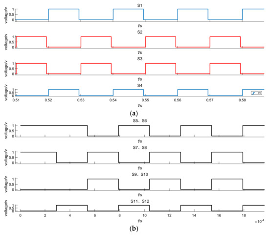
Figure 8.
The proposed inverter working waveform: (a) S1–S4 working waveform; (b) working waveforms of other MOS tubes.
3.2. Capacitance Parameter Analysis
The purpose of the capacitance parameter analysis is to derive the charging and discharging time and to change the voltage on the output side by adjusting the period. It also provides a basis for the selection of capacitance and pulse width modulation, considering that all switches, diodes, capacitors, and inductors have no internal resistance.
RC circuit charging time: As can be seen from the circuit structure diagram in Figure 9, supposing V0 is the initial voltage value on capacitor C, Vin is the voltage value at which capacitor C is fully charged, and Vt is the voltage value on capacitor C at any time t, then
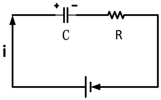
Figure 9.
RC charging circuit structure.
If a battery with a voltage of Vin charges a capacitor C with an initial value of 0 through a resistor R, then at any time t, the voltage on the capacitor is
If it is known that the voltage on the capacitor at a certain moment is Vt, then t can be derived according to the following formula:
Discharge time of RC circuit: It can be seen from the circuit structure diagram of Figure 10 that the capacitor C with the initial voltage of Vin is discharged through R. At any time t, the voltage on the capacitor is
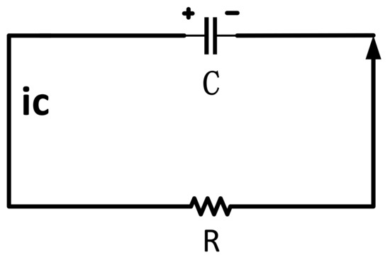
Figure 10.
RC discharge circuit structure.
If it is known that the voltage on the capacitor at a certain moment is Vt, then t can be derived according to the following formula:
The capacitor is connected in series with the DC input power supply Vin to discharge the resistor R; from the circuit structure diagram in Figure 11, the initial voltage value of the capacitor is V0 = Vin, and at any time t, the voltage on the capacitor is
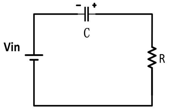
Figure 11.
The capacitor is connected in series with the DC input power to release the voltage to the resistance.
If it is known that the voltage on the capacitor at a certain moment is Vt, then t can be derived according to the following formula:
In particular, when the voltage on the capacitor is 0 (that is, the capacitor is completely discharged), then at this time
By adjusting the charge and discharge cycle of the capacitor, the output voltage can be changed within a certain range. Capacitor selection also has a certain relationship with output frequency, load, and capacitor ripple. A larger capacitor value can prolong the service life of the capacitor. However, an excessively large capacitor will increase the system cost and floor space required. Therefore, it is necessary to consider the relationship between cost and performance, and at the same time, select an appropriate capacitor value in combination with its own output side voltage requirements.
4. Loss Analysis
4.1. Switch Tube Loss
Switching loss includes conduction loss and turn-off loss. The former generally refers to the power loss generated when the power tube is turned from off to on, and the latter generally refers to the power loss generated when the power tube is turned from on to off.
Switch tube conduction loss (this article aims at MOS analysis):
Switch tube turn-off loss (this article aims at MOS analysis):
Here, represents the operating frequency of the switching tube; represents the voltage across the drain-source of the switching tube; and represent the turn-on and turn-off time of the switch tube, respectively; and represent the current before the switch tube is turned on and turned off, respectively.
4.2. Capacitance Loss Analysis
During the operation of the inverter, there will be leakage current flowing through the capacitor, and its loss can be expressed by :
where represents the voltage across the capacitor, and represents the leakage current flowing through the capacitor.
During the operation of the capacitor, there is loss between the plates. The loss tangent of the capacitor plates can be expressed as
Then, the power loss of the capacitor plate:
Here, IC represents the current flowing through the capacitor; represents the equivalent resistance of the plate; represents the tangent value of the loss angle of the capacitor plate; is the capacitive reactance value; and represents the switching tube operating frequency.
5. Simulation and Experiment
5.1. Simulation Result Analysis
In order to verify the correctness of the theoretical analysis of the proposed new inverter, this paper uses the Simulink simulation platform in MATLAB to simulate and analyze the inverter, and set the working frequency of the four Mos tubes of the full bridge to 50 Hz, and the remaining Mos tubes work The frequency is 2 kHz, the capacitance C1 = C2 = 10 μF, R2 = R3 = 5.80 Ω, and the output load R1 = 86.90 Ω. Figure 12 is a waveform diagram of the voltage on the output side of the inverter when the DC input power supply Vin = 4 V. According to the capacitor charging and discharging cycle and demand-side analysis, the output-side voltage was between 6 and 8 V; within the acceptable error, it did not fall below the lowest effective value of 6 V; and the voltage remained stable throughout the inverter working cycle. The average output voltage of the inverter was 6.72 V, and the average current was 80.33 mA. According to our calculations, its efficiency could reach 80%.
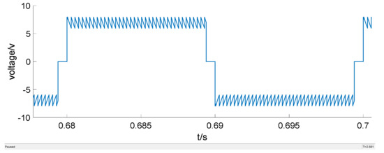
Figure 12.
The inverter output voltage waveform with the circuit operating normally.
Figure 13 and Figure 14 show the simulation comparison between the normal operation of the circuit and the work of S7 and S10 anti-parallel diodes. According to the analysis and comparison diagram, it is obvious that the anti-parallel diode has a significant impact on the inverter output voltage; that is, the average output voltage when compared with the normal operation of Figure 12 is significantly reduced, and there is a significant voltage drop within the specified demand range of 6~8 V. Therefore, it can be concluded that S10, S12, S5, and S7 cannot be connected in reverse parallel with diodes.
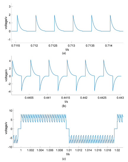
Figure 13.
S7 anti-parallel diode compared with normal working conditions: (a) the circuit works normally, and the voltage is across R3; (b) Voltage across R3 when S7 anti-parallel diode; (c) Inverter output voltage waveform when S7 anti-parallel diode.
Figure 14.
S10 anti-parallel diode compared with normal working conditions: (a) voltage at both ends of the circuit’s normal working capacitor C1; (b) Voltage across capacitor C1 when S10 anti-parallel diode; (c) Inverter output voltage waveform when S10 anti-parallel diodes.
5.2. Experimental Results
In order to validate the proposed structure of the new inverter and its modulation strategy, a small test prototype was built. The test configuration is shown in Figure 15, and Figure 16 shows the physical display diagram of the inverter.
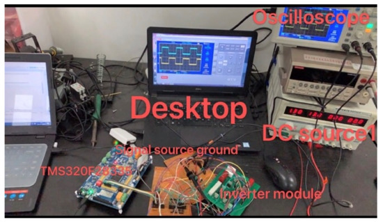
Figure 15.
Test on site.
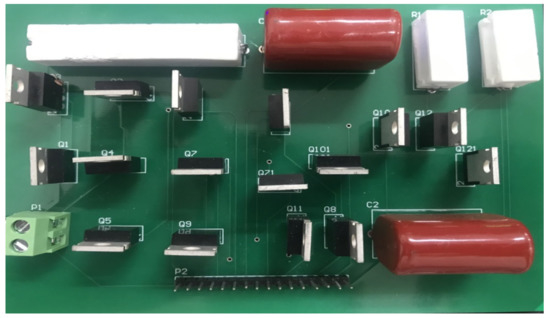
Figure 16.
Inverter physical display.
Figure 17 shows the experimental waveform of the driving voltage of the full bridge (S1, S2, S3, and S4); Figure 18 is a comparison diagram of the alternative switch drive voltage waveforms; and Figure 19 is the inverter output voltage waveform.
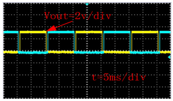
Figure 17.
S1 (S4) and S2 (S3) drive voltage waveform comparison.
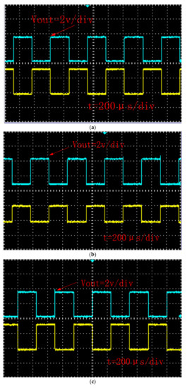
Figure 18.
Comparison of alternative switch drive voltage waveforms: (a) S5 (S6) and S9 (S10); (b) S10 (S9) and S12 (S11); (c) S5 (S6) and S7 (S8).
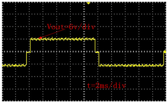
Figure 19.
Inverter output voltage waveform.
DC input voltage was 4 V; DC output voltage was 6–8 V; and output frequency was 50 Hz. From analysis of the results, it can be concluded that the experimental waveforms of the driving signals in Figure 17 and Figure 18 are consistent with those in Figure 8 and the theoretical analysis. The switching frequency of switch tubes S1–S4 is 50 Hz, and the duty cycle is 47%. The deadband can clearly be seen in the figures. The operating frequency of the other switches is 2 kHz. Figure 18 shows the waveform comparison, which is in line with the state of the switch when the system is working normally.
Figure 19 shows the experimental waveform of the output voltage of the inverter when the output frequency is 50 Hz. It can be seen from the figure that the deadband is present correctly, indicating that the full-bridge switch S1–S4 is working normally, and the output voltage waveform of the inverter is ideal and remains stable without falling below the DC input voltage, which is consistent with the results of the simulation experiment. The design of the inverter structure and the feasibility of stable operation are therefore verified.
6. Conclusions
The traditional step-up inverter based on switched capacitors uses the mechanism of capacitors to be charged in parallel and discharged in series in order to achieve the boost effect. When the capacitors are charged in parallel, the inverter output voltage drops. In order to solve this problem, a solution such as the use of inductive energy storage freewheeling has been proposed. However, average voltage and waveform quality on the output side still have defects. Referencing past challenges that have been faced, this paper proposes a new inverter based on switched capacitors, which uses two capacitor modules to charge and discharge alternately. This overcomes the problem of voltage drop on the inverter output side during the transition period from capacitor series discharge to parallel charging. Additionally, the inverter has the characteristics of simple modulation strategy and strong flexibility. Based on the circuit structure and working principle of the inverter, this paper used the Simulink simulation platform in MATLAB to further verify the theoretical feasibility. In addition, experimental verification was carried out on the basis of simulation, which proved the feasibility of the proposed inverter and its modulation strategy.
7. Patents
This article supports the publication of an invention patent: a step-up type non-voltage drop switched-capacitor inverter.
Author Contributions
Conceptualization, H.Q. and J.Z.; methodology, Z.W. and T.X.; software, T.X.; validation, Z.W., T.X., and P.K.; formal analysis, Z.W.; investigation, S.M.; resources, P.K. and S.M.; data curation, H.Q.; writing—original draft preparation, Z.W.; writing—review and editing, Z.W.; supervision, J.Z.; project administration, H.Q.; funding acquisition, T.X. and P.K. All authors have read and agreed to the published version of the manuscript.
Funding
This research was funded by Postgraduate Practice Innovation Program of Jiangsu Province under the grant number [SJCX20_0993].
Institutional Review Board Statement
Not applicable.
Informed Consent Statement
Not applicable.
Data Availability Statement
No new data were created or analyzed in this study. Data sharing is not applicable to this article.
Conflicts of Interest
The authors declare no conflict of interest.
References
- Gang, W.U.; Xinbo, R.U.A.N.; Zhihong, Y.E. Non-isolated High Step-up DC-DC Converters Adopting Switched-capacitor Cell. Proc. CSEE 2015, 35, 442–450. [Google Scholar]
- Shan, L.I.; Wenxu, S.I.; Yan, C.H.E.N.; Sen, C.U.I. Modeling and Analysis of High-frequency Isolated Quasi-Z Source Inverter. J. Power Supply 2018, 16, 52–60. [Google Scholar]
- Qingfa, G.U.; Jie, W. Parameter selection and stability analysis of inverter type microgrid droop controller. Adv. Technol. Electr. Eng. Energy 2017, 36, 34–40. [Google Scholar]
- Wenhua, L.I.; Qi, H.U.; Shannian, L.U.; He, Z.; Hang, Z. Research on the Working Characteristics of the Secondary Boost Inverter. Adv. Technol. Electr. Eng. Energy 2018, 37, 39–44. [Google Scholar]
- Hussan, M.R.; Sarwar, A.; Siddique, M.D.; Mekhilef, S.; Ahmad, S.; Sharaf, M.; Zaindin, M.; Firdausi, M. A Novel Switched-Capacitor Multilevel Inverter Topology for Energy Storage and Smart Grid Applications. Electronics 2020, 9, 1703. [Google Scholar] [CrossRef]
- Guanqian, J.; Zhiyong, L.; Huixia, Y.; Jing, Y. Research review on topological structure of flexible HVDC system. Power Syst. Prot. Control 2015, 43, 145–153. [Google Scholar]
- Zhaohui, D.; Junxi, O.; Bin, B.; Wenguang, C. Design of a frequency adjustable and single-phase output boost type inverter. Electron. Des. Eng. 2017, 25, 110–113. [Google Scholar]
- Yonggao, Z.; Lingtao, K.; Yingying, X. Novel Micro-inverter Power Decoupling Circuit Based on Buck/Boost Circuit. Proc. CSU-EPSA 2020, 32, 29–34. [Google Scholar]
- Shou, L.; Shengyun, J.; Liyong, Y. Research on the Topology of Three-phase Continuous Switching Boost Inverter. Electr. Drive 2018, 48, 31–36. [Google Scholar]
- Lei, C.; Tinglong, P. High gain step-up converter based on switched-capacitor network. Electron. Des. Eng. 2016, 24, 173–177. [Google Scholar]
- Anas, M.; Sarwar, A.; Ahmad, A.; Alam, A.; Ahmad, S.; Sharaf, M.; Zaindin, M.; Firdausi, M. Generalized Structures for Switched-Capacitor Multilevel Inverter Topology for Energy Storage System Application. Appl. Sci. 2021, 11, 1319. [Google Scholar] [CrossRef]
- Nan, L.; Ping, W.; Taizhou, B.; Likun, X.; Cai, Q. Novel high-gain switched capacitor DC boost converter. J. Electr. Power Syst. Autom. 2017, 29, 83–89. [Google Scholar]
- Shiying, H.; Jianfei, C.; Tao, S.; Buyun, M.; Ming, L.; Jia, D. A Single-Switch Step-Up Converter Based on Switched-Capacitor Networks in Parallel. Transact. Chin. Electrotech. Soc. 2015, 30, 242–248. [Google Scholar]
- Luo, F.L.; Ye, H. Positive output cascade boost converters. Proc. Inst. Elect. Eng. Elect. Power Appl. 2004, 151, 590–606. [Google Scholar] [CrossRef]
- Ma Guadalupe Ortiz Lopez, J.; Leyva Ramos, L.H. Multiloop controller for n-stage cascade boost converter. In Proceedings of the 16th IEEE International Conference on Control Applications, Hokkaido, Japan, 6–9 July 2020; pp. 587–592. [Google Scholar]
- Hong, P.; Lejie, T. Boost and Neutral-point Balance Control of Z-source Three-level Inverter Based on SPWM. J. Power Supply 2019, 17, 63–69. [Google Scholar]
- Yikun, J.; Shaoru, Z.; Lingling, L.; Shuai, W. Improved Switching Boost Inverter. Electr. Drive 2016, 46, 33–36. [Google Scholar]
- Li, J.; Jianyong, Z. Z-source photovoltaic grid-connected direct current single-cycle control system. Autom. Electr. Power Syst. 2008, 32, 87–90. [Google Scholar]
- Xuhui, Z.; Xuhui, W.; Feng, Z. A Direct Power Control Scheme for Bi-directional BUCK/Boost Converters in Motor Drive Systems. Proc. CSEE 2012, 32, 15–22. [Google Scholar]
- Cungang, H.; Pei, Y.; Yunlei, Z.; Qunjing, W.; Changbao, Z. Topology and Control Strategy for High-Efficient Non-Isolated Single-Phase Grid-Connected MOSFET Inverter. Transact. Chin. Electrotech. Soc. 2016, 31, 82–91. [Google Scholar]
- Zhao, Q.; Lee, F. High-efficiency, high step-up dc-dc converter. IEEE Trans. Power Electron. 2003, 18, 65–73. [Google Scholar] [CrossRef]
- Wai, R.; Lin, C.; Chu, C. High step-up dc-dc converter for fuel cell generation system. In Proceedings of the 30th Annual Conference of IEEE Industrial Electronics Society, Busan, Korea, 2–6 November 2004; pp. 57–62. [Google Scholar]
- Wu, T.-F.; Lai, Y.-S.; Hung, J.-C.; Chen, Y.-M. Boost convener with coupled inductors and buck-boost type of active clamp. IEEE Trans. Ind. Electron. 2008, 55, 154–162. [Google Scholar] [CrossRef]
- Zhengguo, P.; Yongjie, H.; Yuqi, G. High-Frequency Isolated Grid-Connected Inverter Based on Parallel Resonance. Trans. Chin. Electrotech. Soc. 2018, 33, 322–330. [Google Scholar]
- Covic, G.A.; Boys, J.T.; Kissin, M.L.G.; Lu, H.G. A three-phase inductive power transfer system for roadway-powered vehicles. IEEE Trans. Ind. Electron. 2007, 54, 3370–3378. [Google Scholar] [CrossRef]
- Matsumoto, H.; Neba, Y.; Ishizaka, K.; Itoh, R. Model for a three-phase contactless power transfer system. IEEE Trans. Power Electron. 2011, 26, 2676–2687. [Google Scholar] [CrossRef]
- Dongyuan, Q.; Bo, Z. Composition Principles and Development Trends of Switched Capacitor Converters. Electr. Appl. 2007, 26, 6–12. [Google Scholar]
- Singer, Z.; Emanuel, A.; Erlicki, M.S. Power regulation by means of a switched capacitor. Proc. Inst. Electr. Eng. 1972, 119, 149–153. [Google Scholar] [CrossRef]
- Midgley, D.; Sigger, M. Switched capacitors in power control. Proc. Inst. Electr. Eng. 1974, 121, 703–704. [Google Scholar] [CrossRef]
- Xun, Z.; Ding, H.; He, Z. A Novel Switched-Capacitor Inverter with Reduced Capacitance and Balanced Neutral-Point Voltage. Electronics 2021, 10, 947. [Google Scholar] [CrossRef]
- Umeno, T.; Takahashi, K.; Ueno, F.; Inoue, T. A new approach to low ripple-noise switching converters on the basis of switched-capacitor converters. In Proceedings of the IEEE International Sympoisum on Circuits and Systems, Singapore, 11–14 June 1991; pp. 1077–1080. [Google Scholar]
- Ueno, F.; Inoue, T.; Oota, I.; Harada, I. Power supply for electroluminescence aiming integrated circuit. In Proceedings of the IEEE International Symposium on Circuits & Systems, San Diego, CA, USA, 10–13 May 1992; pp. 1903–1906. [Google Scholar]
- Yang, L.S.; Liang, T.J.; Lee, H.C.; Chen, J.F. Novel high step-up DC-DC converter with coupled-in-ductor and voltage-doubler circuits. In Proceedings of the IEEE Trans on Industrial Electronics, Tainan, Taiwan, 3–6 November 2013; Volume 58, pp. 4196–4206. [Google Scholar]
- Hsieh, Y.P.; Chen, J.F.; Liang, T.J.; Yang, L.S. Novel high step-up DC-DC converter with coupled-inductor and switched capacitor techniques. IEEE Trans Ind. Electron. 2012, 59, 998–1007. [Google Scholar] [CrossRef]
- Fuzhuan, W.; Yongping, D.; Haiquan, W.; Sheng, P.; Geng, W.; Qiangsong, Z.; Tao, H.; Hongli, L. Principle of TMS320F28335 and Its Application in Electrical Engineering; Electronic Industry Press: BeiJing, China, 2020. [Google Scholar]


Publisher’s Note: MDPI stays neutral with regard to jurisdictional claims in published maps and institutional affiliations. |
© 2021 by the authors. Licensee MDPI, Basel, Switzerland. This article is an open access article distributed under the terms and conditions of the Creative Commons Attribution (CC BY) license (https://creativecommons.org/licenses/by/4.0/).