Article

Investigation of Compact Hollow-Anode Discharge Source for Copper Thin Films by Sputtering Processes

1
Institute of Plasma Technology, Korea Institute of Fusion Energy, Gunsan 54004, Korea
2
Department of Electrical Engineering, Hanyang University, Seoul 133791, Korea
*
Author to whom correspondence should be addressed.
Energies 2021, 14(11), 3138; https://doi.org/10.3390/en14113138
Submission received: 13 April 2021 / Revised: 19 May 2021 / Accepted: 23 May 2021 / Published: 27 May 2021

Abstract

:
A compact hollow-anode discharge (HAD) source with a size of 60 mm in radius and 70 mm in length has been developed to stably generate plasma jets for various sputtering processes in semiconductor and display fabrications. A developed HAD plasma source has been investigated by cylindrical electric probes, and the experimental results were compared to the values of numerical calculations. A uniform density discharge model with a geometry factor was proposed to estimate the profiles of plasma parameters. Owing to the difference of absolute magnitude, even with the similar trend of spatial variation, plasma parameters such as electron temperature (Te) and plasma density (ne) measured at z = 3 cm have been calibrated by the values of numerical calculations at the nozzle entrance (z = 0 cm, at the throat of the jet), and the calibration factors for Te and n0 have been deduced by comparing the experimental values to numerical calculations. These are to be explained by the decay mechanism along the axis of the jet with elastic collisions in terms of the mean free path. The developed HAD plasma source was tested for the deposition of Cu thin films with an optimized condition as a plausible application to sputtering processes.

1. Introduction

Plasma jets or ion beam sources have been developed for various material applications, such as plasma enhanced chemical vapor deposition (PECVD), dry etching and plasma surface treatments to improve qualities of substrates and efficiency of processing [1,2,3,4]. A hollow-anode discharge (HAD) source invented by Miljevic [5] was proposed as a plasma source for generating plasma jets. It has provided high-density and high-energy electrons in the hollow-anode region. This is because the probability for collisions of electrons with atoms increases when passing through the hollow anode, and the intensive ionization and excitation of the atoms can be observed [5,6]. As a DC plasma source, it has the advantage of easy operation, low cost and high homogeneity [7]. However, analysis of plasma jets from the hollow-anode plasma is insufficient for material applications, and more practical data are needed in addition to previous research, due to the lack of measurements of plasma parameters and comparison with theory [5,6,8,9].
In this work, a compact HAD source has been developed to stably generate plasma jets for sputtering processes. A uniform density discharge model [10] has been introduced for estimating profiles of the plasma parameters of a present plasma source. The characteristics of the plasma parameters inside plasma jets with various operating conditions were experimentally investigated using IV characteristics measured by cylindrical probes. Experimental results were compared with values of numerical calculations to check the applicability of the developed plasma source, according to the uniform density model for various sputtering processes.

2. Model

To estimate electron temperature (Te) and plasma density (ne) in a cylindrical discharge reactor, a uniform density discharge model by Lieberman is considered [10]. This model assumes a uniform density in the cylindrical plasmas with a sharp boundary at the sheath edge (i.e., a box shape). Electrons as the major energy carrier are assumed to have the Maxwell–Boltzmann distribution. Te is calculated using the particle balance between the total surface particle losses and the total volume ionization, while ne is calculated using an energy balance between the total power absorbed and the total power losses. Considering the particle balance to determine Te, the equilibrium equation is given as [10]:
n 0 u B A e f f = η i z n g n 0 π R 2 L ,
where A e f f = 2 π R 2 h L + 2 π R L h R is the effective area for particle losses. n 0 ,   u B ,   η i z ,   n g ,   R ,   and L are the plasma density of the central reactor region, Bohm speed, the ionization rate constant, the neutral gas density, radius and axial length of the chamber, respectively. Using the definition of the Bohm speed,   u B = T e / m i 1 / 2 where m i is the mass of an ion, the electron temperature can be obtained as:
T e = m i u B 2 = m i π R 2 L A e f f n g η i z 2 = m i n g 2 η i z 2 ξ e f f 2 ,
where ξ e f f is an effective plasma size for particle losses, which is given as ξ e f f   π R 2 L / A e f f = 0.5 R L / R h L + L h R . It can be estimated using Godyak’s formulae of hL and hR: h L n s L / n 0   0.86 3 + L / 2 λ i 1 / 2 for the axial sheath edge density (nsL) and h R n s R / n 0   0.8 4 + R / 2 λ i 1 / 2 for the radial sheath density (nsR), where λ i is ion mean free path [10,11,12]. The ionization rate constant is given as [10]:
η i z = σ 0 v ¯ e 1 + 2 T e E i z e E i z / T e ,
where σ 0 = π 1 4 π ϵ 0 E i z 2 is the initial condition for the Thomson cross-section, and v ¯ e = 8 T e π m 1 2 is the average electron speed. E i z and ϵ 0 are the ionization energy of gas and permittivity of free space, respectively. The uniform density model assumes the sharp fall near the wall, while the practical plasma density profile would follow a Gaussian distribution. Between the uniform distribution and the Gaussian distribution, there is a non-negligible and physically important difference: Uniform distribution assumes that the density at the boundary or at the sheath is the same as the density of the center or equilibrium ( n 0 ) by assuming that the sheath potential is the same as the plasma potential ( V s = V p : n e r = s = n 0 exp V s V p = n 0 ) . This is a common assumption that Child, Langmuir, Chen, Franklin and Lieberman have already made [10,13]. However, the real boundary condition at the sheath is the Bohm condition, i.e., the ion speed at the sheath is the Bohm speed ( u B = T e / m i 1 / 2 ) if Ti = 0, which leads to the sheath potential, which should be such that V s V p = T e / 2 e , which again makes the sheath density n s = n 0 / 2 . Thus, under Bohm’s criterion [10,13,14], the boundary density or sheath density should not be n 0 , but rather n 0 / 2 , which makes the uniform source distribution un-acceptable, physically [14]. Therefore, although a Gaussian profile is not the only physical one, it would be a better one than the uniform profile. By assuming a Gaussian distribution for a plasma density profile, this indicates that plasma particle losses are smaller than those of the uniform density model as shown in Figure 1. Therefore, to compensate for the difference of loss of particles and energy between the uniform and Gaussian models, we need to introduce a geometry factor (k) to the uniform model by reducing the effective area of loss ( A e f f ), or by increasing effective plasma size ( ξ e f f ). The effect of k is to be shown in the results of numerical calculations for plasma density and electron temperature. From Equation (2), Te can be rewritten as:
T e = m i n g 2 η i z 2 ξ e f f k 2 .  
Assuming uniform energy loss at all surfaces, plasma density (n0, in the central region of plasma source) from the energy balance can be calculated by equating the total power generation ( P g ), which is absorbed into the electrons [10]:
P g = n 0 u B A e f f E T ,
where total energy loss ( E T ) is given as E T = E i + E e + E c [eV] and the other constants are the same as mentioned previously. Mean kinetic energy loss per ion loss, Ei, is given as V s + 0.5 T e for argon gas. V s = T e ln m i / 2 π m e 1 / 2 is the sheath voltage, where m e is the mass of an electron when ion and electron fluxes which are balanced in the steady state are assumed. Mean kinetic energy loss per electron loss, Ee, is approximated as 2 T e . Collisional energy loss per electron–ion pair created ( E c ) is indicated as [10]:
E c = [ η i z E i z + η e x E e x + η e l 3 m e / m i T e ] / η i z ,
where η i z ,   η e x , η e l and E e x are rate constants for ionization, excitation, elastic scattering and excitation energy, respectively. In the RHS of Equation (6), the numerator means collisional energy losses due to ionization, excitation and elastic scattering against neutral atoms. Finally, for estimation of n0, Equation (5) is rewritten as:
n 0 = P g / E T A e f f T e / m i 1 / 2 ,  
where Te for calculation of u B is used from Equation (4), where k is applied to check its effects for the compensation of A e f f for plasma particle losses. To simulate plasma parameters, the discharge current between electrodes was assumed to be given by the Child–Langmiur space-charge limited equation [10,15,16], along with the following conditions: radius of cylindrical source (R) = 10 mm, axial length (L) = 10 mm and argon gas as working gas.

3. Experiment

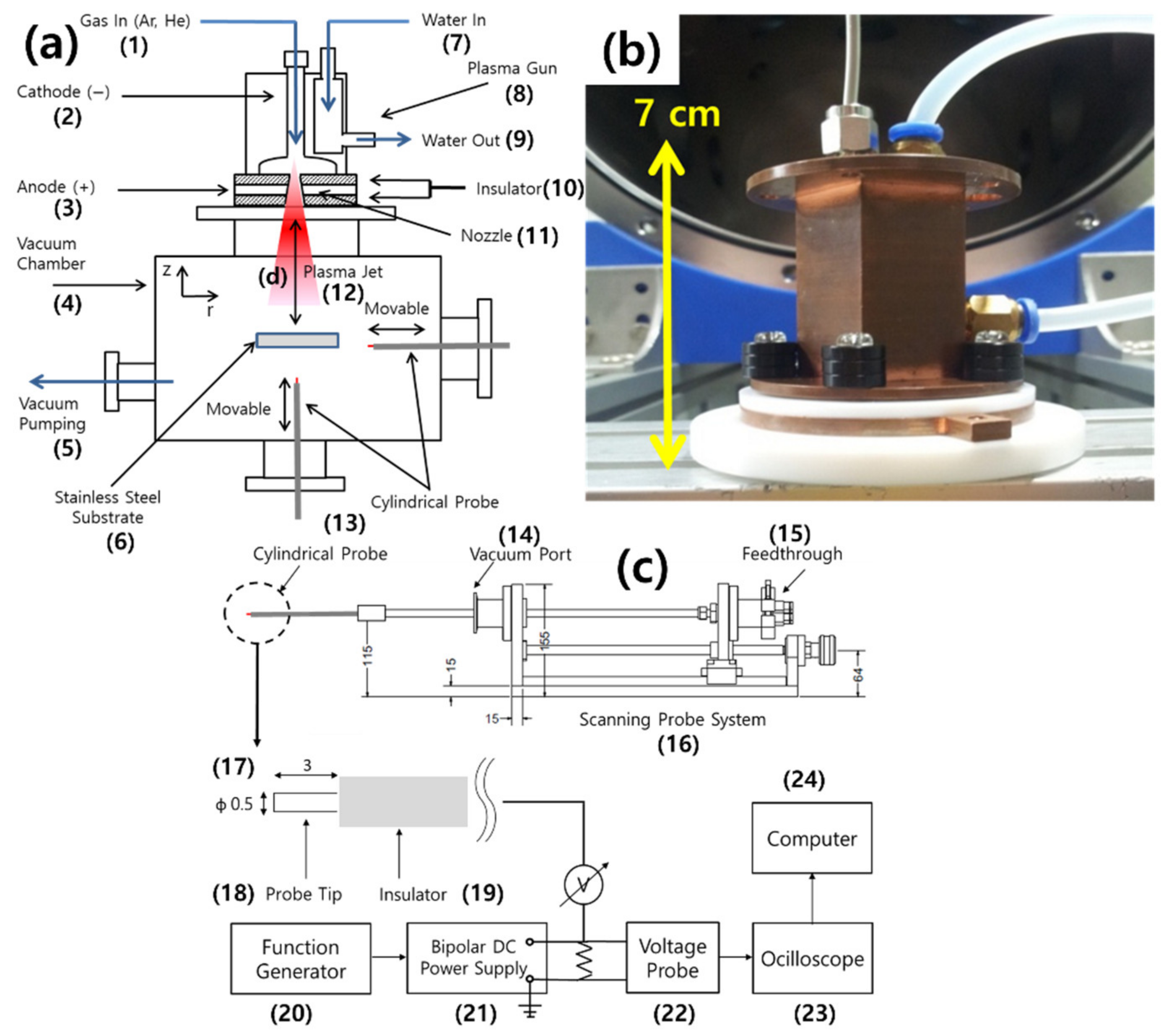
The operating principle, schematic view and photograph of the developed HAD source for generating plasma jets with the experimental set-up are shown as Figure 2 and Figure 3. The developed source has a compact size with a length of 70 mm and radius of 60 mm. The cathode of HAD has a hemisphere shape with a diameter of 20 mm, while the anode has a narrow throat with a diameter of 3 mm and a wide exit with 9 mm in diameter. Oxygen-free electrolytic coppers (OFC) are used for electrodes. To cover 98% of the anode area, excluding the nozzle vicinity, a Teflon (PTFE) insulator between electrodes is used with a thickness of 3 mm. A water-cooling system is introduced inside the cathode to prevent and reduce thermal damage from plasmas. Argon gases are fed into the plasma source, where the pressure is approximately 100 Pa (0.8 Torr) at a flow rate in a 1–100 sccm range, through a stainless tube fixed by vacuum fitting. Figure 3b is a photograph of the plasma source after fabrication. The exposed anode area for generating hollow-anode plasma at the nearby nozzle throat, such as a plasma ball [6], is about 13 mm2. For the ignition of plasmas between electrodes, the DC power was supplied to electrodes with an applied voltage of 0–450 V and a discharge current of 0–150 mA.
At 0.4~7 Pa (3~5 × 10⁻³ Torr), parameters such as Te and ne inside plasma jets generated from the nozzle throat were measured by cylindrical scanning probes [17,18], which were made of a molybdenum tip with 0.5 × 3 mm (dia. × length) and an Al2O3 ceramic holder with 3 mm of diameter. The current–voltage (IV) characteristic curve is obtained from collected ion and electron currents by sweeping the probe bias voltage from −100 V to + 100 V for the measurement of scanning the probe system with a single probe tip, as shown in Figure 3b. T e is obtained from the slope of the IV characteristic curve, and n e can be determined from the ion saturation current ( I s a t = α n e e A s K T e / m i ) with an assumption of T e T i at non-thermal plasma, where α , e, A s and K are coefficients for the collective ion saturation current, electron charge, sheath area and Boltzmann constant, respectively. A s A p (probe tip area 2 × 10 4 cm2) is assumed and α 0.61 is used for un-magnetized plasmas [19,20]. To reduce the signal uncertainty, two cylindrical probes are used, as shown in Figure 3. One scans for radial direction and the other scans for axial direction. The average value of plasma parameters measured from two cylindrical probes is used.

4. Results

Figure 4 shows the VI characteristics of the plasma jets with various gas flow rates. At each specified gas flow rate, one voltage transition occurred within a specified threshold of the applied voltage, which was increased as gas flow rates decreased. After the voltage transition, generated plasma jets became more stable with high discharge currents. Applied voltages were maintained as almost constant, even when discharge currents increased up to 150 mA, showing fully developed state plasmas between the electrodes. This may be explained by a “layered-glows mode” which plays a crucial role on the relation of higher discharge currents with applied voltages only at a hollow-anode plasma source [9]. Hence, we intensively focused on plasma jets, generated by the high current mode, after voltage transition.
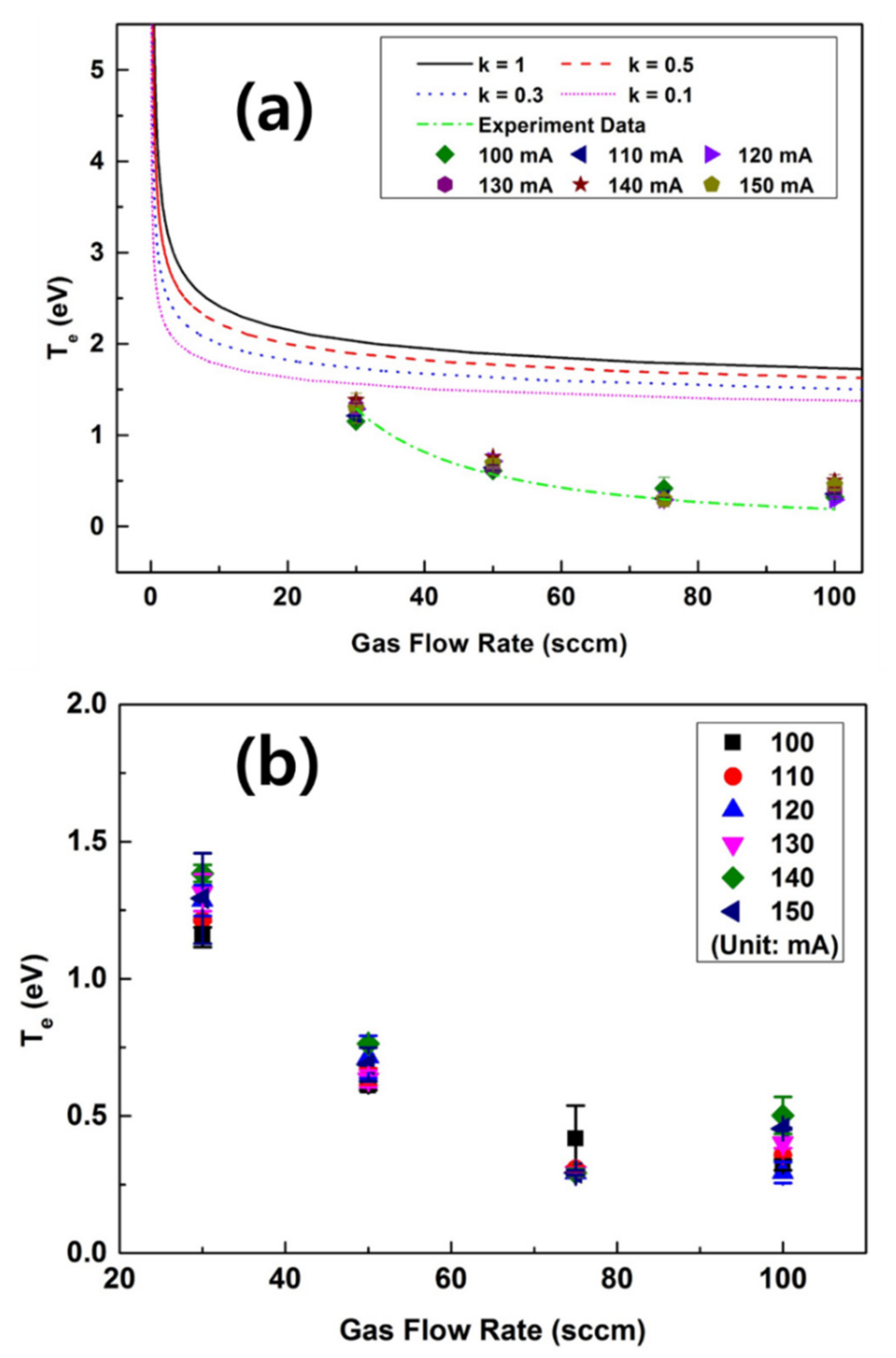
Figure 5a shows the experimental results of Te measured by a cylindrical electric probe, which are to be compared to values of numerical calculations according to gas flow rates. The various k values were checked, such as k = 0.1–1, e.g., k = 0.5 means that the amount of plasma particle losses is half that of those by the uniform density model (k = 1). Comparing this to the original uniform density discharge model by applying k = 0.1, the absolute simulated Te values come closer to the experimental results with similar tendencies than the original model (i.e., k = 1) but need further analysis to optimize the model. Increasing gas flow rates produced lower Te of the plasma jets. Significant effects of discharge currents on Te are not observed, as shown in Figure 5b. In our developed HAD source, Te was nearly saturated at approximately 0.45 eV at the gas flow rate of 75 sccm, irrespective of the geometry factor k. Experimental results showed lower electron temperatures than values of numerical calculations, which clearly seems to be caused by the difference of position for the numerical calculations from that of the experimental measurement by an electric probe. The value of numerical calculations was given at the center of plasma source (z = 0 cm), while the one measured is at the middle of plasma jet (z = 3 cm) generated from the nozzle.
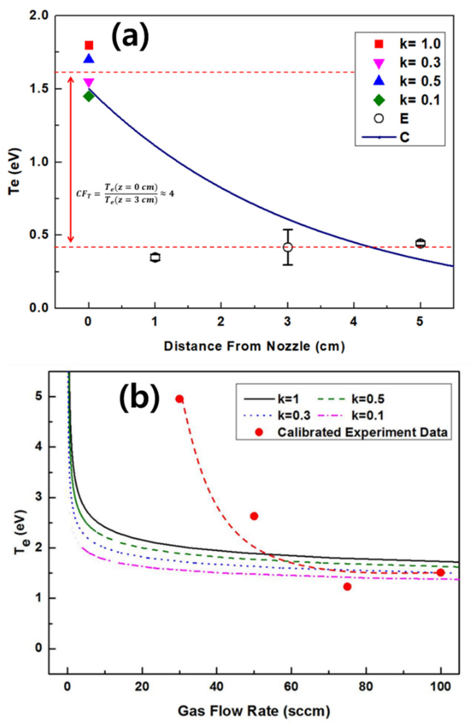
To compensate for the difference due to the positions of measurement and numerical calculations, a calibration factor ( C F T ) is introduced to Te profiles as C F T = T e   ( z 0 , s i m u l a t i o n ) / T e   z 3 c m , e x p e r i m e n t . By using the Te profiles given as functions of distance (z) from the nozzle, a calibration factor is obtained, as shown in Figure 6a. The calibration factor for Te ( C F T ) is given by taking the average of the ratio: C F T 4 . As for the calibration factors of Te ( C F T ), one could consider the small angle elastic scattering of charged particles via Coulomb collisions [21], where the ratios of different collision frequencies are given in terms of momentum relaxation rates ( ν m / ν 0 e / i ) and energy relaxation rates ( ν ε / ν 0 e / i ) as the following: ν m e / i / ν 0 e / i = 1 , ν m e / e / ν 0 e / i = 1.2 , ν ε e / i / ν 0 e / i = 2 ( m e / m i )   ~   10 4 and ν ε e / e / ν 0 e / i = 0.6 , where ν is the elastic collision frequency. Then, the ratio of total energy transfer to total momentum (velocity) transfer is calculated as ν m /   ν ε = ( ν m e / e + ν m e / i ) / ν ε e / e + ν ε e / i = 3.7   . Since the mean free path is inversely proportional to the collision frequency ( λ n   1 / ν ), the spatial variation of electron temperature can be expressed as:
T z = T 0 exp z / λ T   = T 0 exp [ z / { ( ν m / ν ε ) λ n } ] .
Hence, the calibration factor of electron temperature is calculated as C F T = T 0 / T 3 c m = 2.5 , which is close to our experimental calibration factor of electron temperature, C F T   ~   4 . Here z = 3 cm, ν m /   ν ε = 3.7   and λ n = 0.9   cm are used. Similar values of calibration factors between the numerical calculations and experiments indicate our approach as being valid and relevant. Figure 6b shows the compensated Te profiles comparing experimental data with values of numerical calculations, showing a similar scale and trend, yet there is another difference in terms of the gas flow rate, which is for the refinement of the present layered-glows model, with inclusion of the tremendous loss of electron energies by frequent collisions at low discharge voltages.
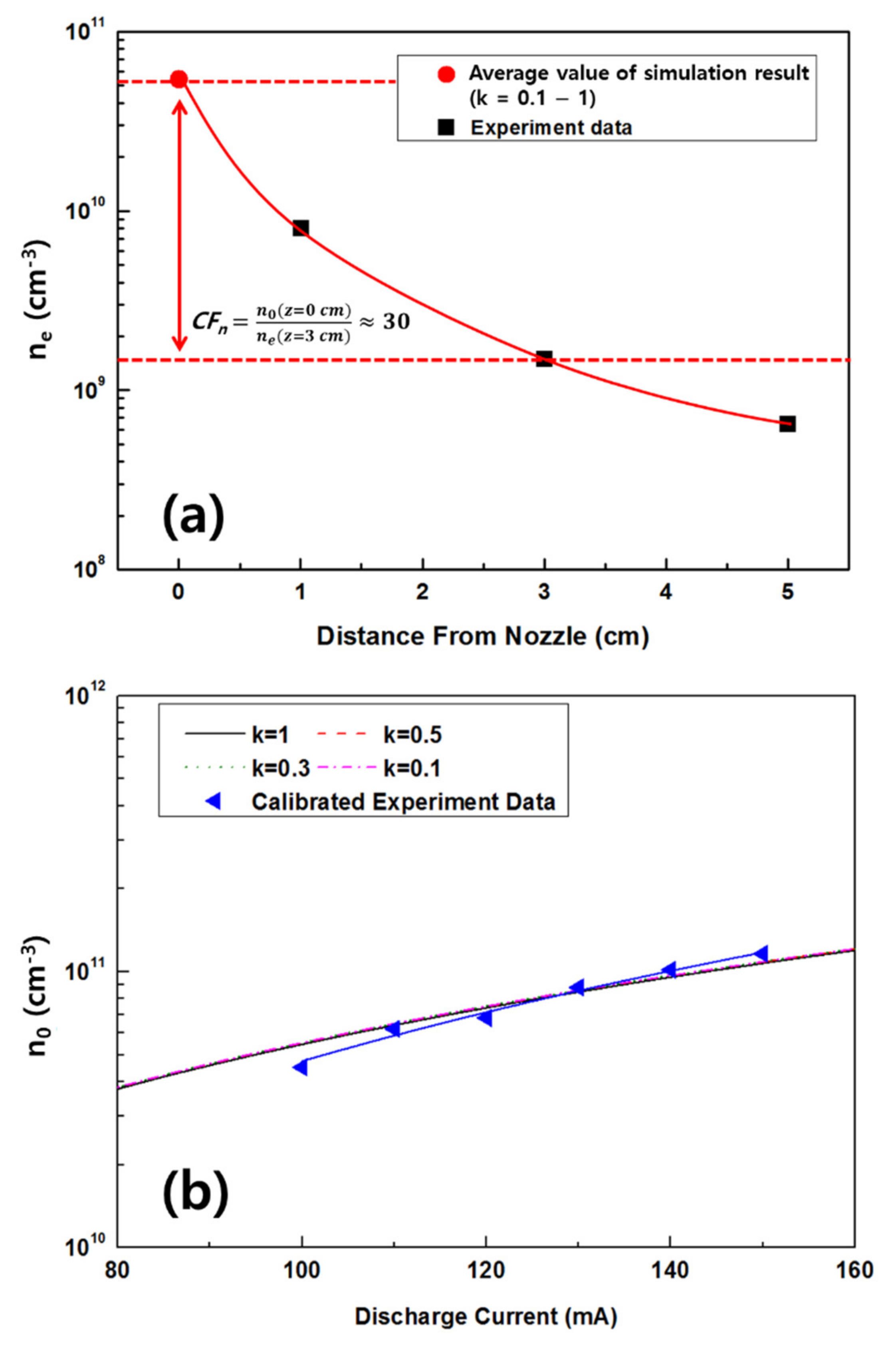
The profiles of plasma density, the numerical calculation results of the center of plasma source and the measurement data at 3 cm from a nozzle throat, which depend on the discharge currents with various gas flow rates, are shown in Figure 7. In comparison with the numerical calculation values, the experimental results were more dependent on gas flow rates. Plasma density measured by a cylindrical probe, which was slightly increased by raising discharge currents, shows a similar tendency with numerical calculation results. To check the effects of k to n0, the numerical calculation values in Figure 7a are magnified as shown in Figure 7b. By comparing the difference of experimental data with the numerical calculation values, the effects of k seem to be insignificant, but n 0 slightly increases as much as k decreases. Based on Figure 6b and Figure 7b, it does affect the analytic values of electron temperature and density: ΔTe/avg. Te ~ 0.25 = 25% and Δ n 0 / avg . n 0   ~ 0.1 = 10%. Thus, the k factor seems to affect the numerical calculation results of electron temperature more than those of density. The difference of absolute values between numerical calculations and experimental results is for the same reasons as with Te as mentioned above, i.e., the difference of measured and simulated positions. To easily understand the reason and calibrate ne profiles for position difference, the relation between the n0 and ne according to distances (1 cm, 3 cm and 5 cm) from the nozzle throat is shown in Figure 8a. As a function of the distance from the nozzle, n0 profiles seem to be in exponential decay. This means that calibration is required for the correct comparison of experiment data with numerical calculation values at the same position. The calibration factor for n 0 is given by taking the average of the ratio: C F n = n 0 z 0 , s i m u l a t i o n / n e z 3 c m ,   e x p e r i m e n t 30 . Calibrated experimental data seem to be fairly matched with numerical calculation results, as shown in Figure 8b. As for the calibration factors of Te and ne ( C F T and C F n ), one could expect the exponential decay of density and temperature along the axial direction of jets due to collisions since the density of plasma jets is strongly dependent on the mean free path ( λ n ) which could be expressed as
n z = n 0 exp z / λ n ,  
where n 0 is the density at the exit of the plasma jet ( z = 0 ). Applying the relation by Liebermann for the mean free path λ n = 1 / 330 p (p in Torr, λ n in cm) at Ti ~ 0.01 eV [10,22] to our experimental condition (gas flow rate: 75 sccm at 3.5 × 10⁻³ Torr), which is nonthermal plasma with low energy ions, we can obtain the calibration factor of the density profile as C F n = n 0 / n 3 c m = 32 . This is very close to our experimental calibration factor of plasma density, C F n   ~     30 . From this calibration factor, one can deduce the mean free path as the following: λ n = z / ln n 0 / n 3 c m = 3 / ln 30 = 0.9   cm .
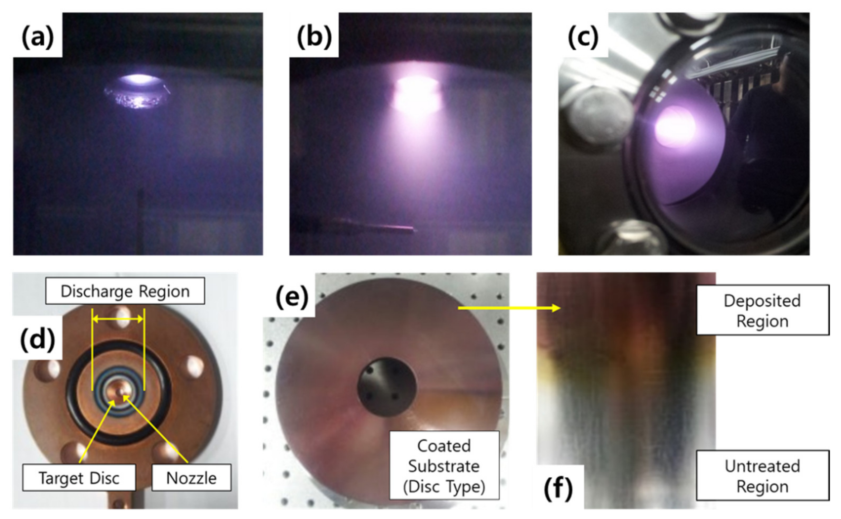
Finally, the applicability of the developed plasma source was checked for sputtering processes. Figure 9 shows the formation of the plasma jets produced by using a DC power, a pulsed DC power and a RF power for material application such as metal thin films. The deposition of copper thin films on a stainless-steel substrate with the operating source condition is given as the following: ne ~   3 × 10 9 cm3; Te ~ 0.45 eV at 3 cm from the nozzle exit; gas flow rate ~ 75 sccm, discharge currents ~ 150 mA and the applied voltage ~ 300 V. From the etched target disc, as shown in Figure 9d, we predict that the efficiency of sputtering processes by ions generated from Cu, Pt, ITO or the other metal target discs could be improved. This is because this concept uses higher-density plasmas near a hole of anode, rather than a commercial source used by glow discharge plasmas. This is explained by the formation of stable plasma jets with a high discharge current after the voltage transition, in the section of VI characteristics. Additionally, the report [9] of experimental analyses on the plasma phenomena inside the hollow-anode discharge source to maintain the discharge at a higher sustaining current, with high efficiency in constricted DC plasmas, is a clearer rationale for improving the efficiency of sputtering processes by the developed plasma source.
In future works, we will conduct sputtering processes using the developed plasma source and investigate its treatment on various substrates for verification of experimental conditions once more.

5. Conclusions

A new compact plasma jet with the concept of a HAD structure has been developed for an application to sputtering processes. As a DC plasma source, it has a small size with a tiny plasma volume (R = 60 mm, L = 70 mm, plasma volume = 4 × 103 mm3) and a high plasma density (ne ~   3 × 10 9 cm3). It is analyzed by IV curves of discharge, electric probe measurement and numerical analysis with a collisional model. A uniform density discharge model was used to estimate the plasma parameters. To compensate the ideal uniform discharge model with respect to the plausible Gaussian profile of density, a geometry factor (k) was introduced. Plasma jets generated by the developed plasma source were experimentally investigated using voltage–current (VI) characteristics and the measurement of electric probes. After a certain voltage transition, the plasma jets became very stable with a high discharge current, which could be explained by a layered-glows model. By applying k = 0.1, Te became closer to the experimental results than the ideal model and showed similar tendencies, while n0 seems to be insensitive to the density profile. To compensate for the discrepancy due to the different position of measurement from that of numerical calculations, calibration factors for Te and ne are introduced: C F T = 4 ,   C F n = 30 , which are to be explained by the decay mechanism of density and temperature along the axial direction in terms of elastic scattering and mean free path. Experimental results with the calibration of position difference for plasma parameters such as Te and n0 became very similar to the numerical calculation values at the same position (z = 0 cm). With the optimized conditions, the developed HAD source was tested for the deposition of copper thin films, which showed a plausible application to various sputtering processes.

Author Contributions

Conceptualization, I.-J.K. and K.-S.C.; methodology, I.-J.K.; software, I.-J.K. and I.-S.P.; validation, J.-H.K. and K.-S.C.; formal analysis, I.-J.K. and I.-S.P.; investigation, I.-J.K., J.-H.K. and I.-S.P.; data curation, I.-J.K. and K.-S.C.; writing—original draft preparation, I.-J.K.; writing—review and editing, I.-J.K. and K.-S.C.; visualization, I.-J.K.; supervision, J.-H.K. and K.-S.C.; project administration, I.-S.P.; funding acquisition, J.-H.K. and K.-S.C. All authors have read and agreed to the published version of the manuscript.

Funding

This research was supported by R&D Program of “Plasma Convergence & Fundamental Research (1711124796)” through the Korea Institute of Fusion Energy (KFE) and funded by the Government funds, Republic of Korea. This research was supported by the National R&D Program through the National Research Foundation of Korea (NRF) funded by the Ministry of Science, ICT and Future Planning (2019M1A7A1A03088471).

Institutional Review Board Statement

Not applicable.

Informed Consent Statement

Not applicable.

Data Availability Statement

The data presented in this study are available on request from the corresponding author.

Conflicts of Interest

The authors declare no conflict of interest.

References

  1. Kang, I.J.; Joa, S.B.; Lee, H.J. Study on effect of plasma surface treatments for diamond deposition by DC arc plasmatron. J. Nanosci. Nanotechnol. 2013, 13, 7370–7375. [Google Scholar] [CrossRef] [PubMed]
  2. Kang, I.J.; Ko, M.G.; Yang, J.K.; Lee, H.J. Plasma surface treatments by using a dielectric barrier discharge for the deposition of diamond films. J. Korean Phys. Soc. 2013, 63, 199–205. [Google Scholar] [CrossRef]
  3. Terasawa, T.; Saiki, K. Growth of Graphene on Cu by Plasma Enhanced Chemical Vapor Deposition. Carbon 2012, 50, 869–874. [Google Scholar] [CrossRef]
  4. Jeong, J.Y.; Babayan, S.E.; Tu, V.J.; Park, J.; Henins, I.; Hicks, R.F.; Selwyn, G.S. Etching materials with an atmospheric-pressure plasma jet. Plasma Source Sci. Technol. 1998, 7, 282–285. [Google Scholar] [CrossRef]
  5. Miljevic, V.I. Hollow anode ion–electron source. Rev. Sci. Instrum. 1984, 55, 931–933. [Google Scholar] [CrossRef]
  6. Anders, A.; Anders, S. The working principle of the hollow-anode plasma source. Plasma Source Sci. Technol. 1995, 4, 571–575. [Google Scholar] [CrossRef]
  7. Granda-Gutiérrez, E.E.; López-Callejas, R.; Peña-Eguiluz, R.; Valencia, A.R.; Mercado-Cabrera, A.; Barocio, S.R.; de la Piedad-Beneitez, A.; Benítez-Read, J.S.; Pacheco-Sotelo, J.O. V-I curves and plasma parameters in a high density DC glow discharge generated by a current-source. J. Phys. Conf. Ser. 2008, 100, 062019. [Google Scholar] [CrossRef]
  8. Abdelsalam, F.W.; Helal, A.G.; Saddeek, Y.B.; Abdelrahman, M.M.; Soliman, B.A. Investigation and application of hollow anode glow discharge ion source. Nucl. Instrum. Methods Phys. Res. Sect. B 2010, 268, 3464–3467. [Google Scholar] [CrossRef]
  9. Park, Y.-S.; Hwang, Y.S. Enhancement in ion beam current with layered-glows in a constricted dc plasma ion source. Rev. Sci. Instrum. 2010, 81, 02B309. [Google Scholar] [CrossRef] [PubMed]
  10. Lieberman, M.A.; Lichtenberg, A.J. Principles of Plasma Discharges and Materials Processing, 2nd ed.; Wiley: Hoboken, NJ, USA, 2005. [Google Scholar]
  11. Godyak, V.A. Soviet Radio Frequency Discharge Research; Delphic: Falls Church, VA, USA, 1986. [Google Scholar]
  12. Kimura, T.; Ohe, K. Global model of inductively coupled Ar plasmas using two-temperature approximation. J. Appl. Phys. 2001, 89, 4240–4246. [Google Scholar] [CrossRef]
  13. Chen, F.F. Introduction to Plasma Physics and Controlled Fusion, 3rd ed.; Springer: Los Angeles, CA, USA, 2016. [Google Scholar]
  14. Hutchinson, I.H. Principles of Plasma Diagnostics, 2nd ed.; Cambridge University Press: New York, NY, USA, 2002. [Google Scholar]
  15. Green, T.S. Beam Formation and Space Charge Neutralisation. IEEE Trans. Nucl. Sci. 1976, NS-23, 918–928. [Google Scholar] [CrossRef]
  16. Abdelsalam, F.W.; Helal, A.G.; Abdelrahman, M.M.; Soliman, B.A. Operating characteristics of the hollow anode glow discharge ion source. Vacuum 2010, 84, 405–409. [Google Scholar] [CrossRef]
  17. Chung, K.-S.; Hong, S.-H.; Chung, K.-H. Measurements of Plasma Flow Velocity in DC Plasma Jets Using Perpendicular and Parallel Mach Probes. Jpn. J. Appl. Phys. 1995, 34, 4217–4222. [Google Scholar] [CrossRef]
  18. Kim, J.-W.; Cho, S.-G.; Bae, M.-K.; Kim, H.-J.; Chung, T.H.; Chung, K.-S. Analysis of Electron Temperature in DC Ar/SF6 Plasma Using Cylindrical and Planar Probes. Jpn. J. Appl. Phys. 2013, 52, 11NC03. [Google Scholar] [CrossRef]
  19. Kang, I.J.; Bae, M.-K.; Lho, T.; Chung, K.-S. Experimental investigation of free and bounded presheaths in weakly magnetized plasmas. Curr. Appl. Phys. 2017, 17, 358–365. [Google Scholar] [CrossRef]
  20. Chen, F.F. Langmuir probe analysis for high density plasmas. Phys. Plasmas 2001, 8, 3029–3041. [Google Scholar] [CrossRef] [Green Version]
  21. Callen, J.D. Model of Plasma Confinement and Heating in Tokamaks; University of Wisconsin: Madison, WI, USA, 1989. [Google Scholar]
  22. Choi, Y.-S.; Woo, H.-J.; Chung, K.-S.; Lee, M.-J. Determination of Plasma Flow Velocity by Mach Probe and Triple Probe with Correction by Laser-Induced Fluorescence in Unmagnetized Plasmas. Jpn. J. Appl. Phys. 2006, 45, 5945–5950. [Google Scholar] [CrossRef]
Figure 1. Comparison of plasma density distribution for the complement of A e f f for plasma particle losses: (a) uniform density discharge model and (b) plasma density assuming Gaussian distribution.
Energies 14 03138 g001
Figure 2. Principle of hollow-anode plasma source for sputtering processes. It uses a high-density plasma (plasma ball) formed near a hollow and after an applied voltage transition.
Energies 14 03138 g002
Figure 3. (a) Schematic view of a source system, (b) photograph of the developed source and (c) scanning probe system with the electric probe for measurement of plasma parameters. The distance (d) is 3 cm between the nozzle and substrate. (1) Gas in, (2) cathode, (3) anode, (4) vacuum chamber, (5) vacuum pumping, (6) stainless steel substrate, (7) water in, (8) plasma gun, (9) water out, (10) insulator, (11) nozzle, (12) plasma jet, (13) cylindrical probe, (14) vacuum port, (15) feedthrough, (16) scanning probe system, (17) 0.5 × 3 mm (dia. × length), (18) probe tip, (19) insulator, (20) function generator, (21) bipolar DC power supply, (22) voltage probe, (23) oscilloscope and (24) computer.
Energies 14 03138 g003
Figure 4. VI characteristics (applied voltage vs. discharge current) of the developed plasma source with various gas flow rates.
Energies 14 03138 g004
Figure 5. The Te profiles according to gas flow rates: (a) for comparing numerical calculations with the geometry factor (k) = 0.1–1 (z: 0 cm, at a center of plasma source) and experimental results (z: 3 cm, at plasma jet: 3 cm from a nozzle throat) and (b) experimental results with various discharge currents in detail.
Energies 14 03138 g005
Figure 6. The Te profiles: (a) according to distance from nozzle (argon gas flow rate: 75 sccm) to calibrate position difference for correct comparison of numerical calculation results with experiment data and (b) comparison of numerical calculation results with calibrated experiment average values of 100–150 mA as function of gas flow rates compensated for position difference (z: 0 cm). (E) and (C) in this figure legend are experiment and calculation results by Equation (8), respectively.
Energies 14 03138 g006
Figure 7. (a) The n0 profiles as a function of discharge currents with various gas flow rates for comparing numerical calculations (z: 0 cm, at a center of plasma source and k: 0.1–1) and experimental results (z: 3 cm, at plasma jet from a nozzle exit) and (b) numerical calculation results in detail.
Energies 14 03138 g007
Figure 8. (a) The ne profiles according to distance from nozzle (argon gas flow rate: 75 sccm) to calibrate position difference for correct comparison of numerical calculation results with experiment data and (b) comparison of numerical calculation results with calibrated experiment data as a function of discharge currents at the same position (Z: 0 cm, argon gas flow rate: 75 sccm).
Energies 14 03138 g008
Figure 9. The developed hollow-anode plasma source for material applications: formation of plasma jets by using (a) a DC power (25 W), (b) a pulsed DC power (40 W), (c) RF power (100 W), (d) the used anode and target disc (e) and (f) copper thin films deposited on a stainless steel.
Energies 14 03138 g009
Publisher’s Note: MDPI stays neutral with regard to jurisdictional claims in published maps and institutional affiliations.