Abstract
This paper presents a full-bridge active-clamp forward-flyback (FBACFF) converter with an integrated transformer sharing a single primary winding. Compared to the conventional active-clamp-forward (ACF) converter, the proposed converter has low voltage stress on the primary switches due to its full-bridge active-clamp structure, which can leverage high performance Silicon- metal–oxide–semiconductor field-effect transistor (Si-MOSFET) of low voltage rating and low channel resistance. Integrating forward and flyback operations allows the proposed converter to have much lower primary root mean square (RMS) current than the conventional phase-shifted-full-bridge (PSFB) converter, while covering wide input/output voltage range with duty ratio over 0.5. The proposed integrated transformer reduces the transformer conduction loss and simplify the secondary structure of the proposed converter. As a result, the proposed converter has several advantages: (1) high heavy load efficiency, (2) wide input voltage range operation, (3) high power density with the integrated transformer, and (4) low cost. The proposed converter is a very promising candidate for applications with wide input voltage range and high power, such as the low-voltage DC (LDC) converter for eco-friendly vehicles.
1. Introduction
Nowadays, eco-friendly vehicles such as hybrid electric vehicle and electric vehicle have been researched and developed to satisfy the strengthened CO2 emission regulations as well as to increase fuel economy [1,2,3]. A lot of power conversion systems have been studied for eco-friendly vehicles. These power conversion systems require not only a high efficiency to improve the fuel economy but also a high power density because those are installed in the engine and trunk rooms of eco-friendly vehicles. Moreover, the price of eco-friendly vehicles is much higher than that of the traditional vehicles due to additional power conversion systems, i.e., drive motor, inverter, converters, and battery. Therefore, reducing the production cost is also one of the most important design considerations for eco-friendly vehicles. Furthermore, the power consumption caused by electronic devices of vehicles has been rapidly increased due to the remarkable improvement of information technology and development of electronic system such as advanced driver assistance system (ADAS), motor drive steering system (MDPS), traction control system (TCS), information devices, etc. [4].
To supply power to electronic devices of vehicles, a LDC converter that charges low voltage (LV) battery (e.g., 13.6 V) with the energy stored in high voltage (HV) battery (e.g., 300 V) is commonly used in eco-friendly vehicles. The LV battery is usually controlled to maintain its nominal voltage. Namely, the LDC converter should be designed to cover wide input voltage range of the HV battery. Due to the increased power consumption of high-performance electronic devices (ADAS, MDPS, and so on) in vehicles, the discharging current of the LV battery has been increased. Accordingly, to maintain the LV battery in normal range, the nominal output current of the LDC converter, i.e., charging current of the LV battery, has been also continuously increased. As a result, it is getting important for the LDC converter to achieve higher heavy load efficiency. Currently, plug-in hybrid electric vehicles (PHEVs) usually adopt a HV battery with 240–413 V (nominal 360 V), and HEVs do a HV battery with 200–310 V operating range (nominal 270 V). Both uses approximated 13.6 V LV battery. In addition, the LDC converter is designed up to 2 kW meaning very high output current of 140–160 A.
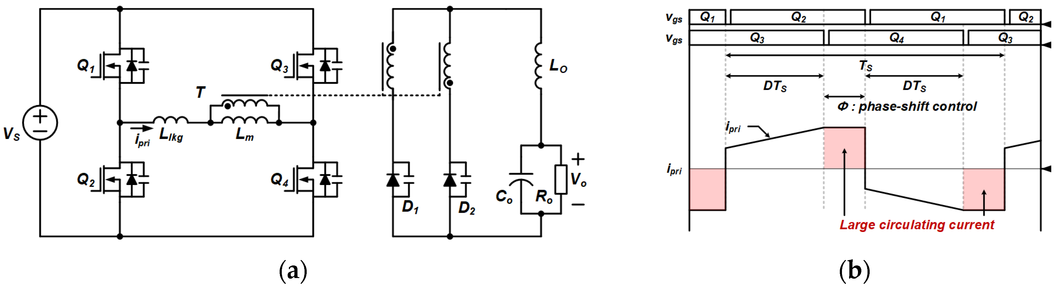
In order to achieve high efficiency and high power density under wide input voltage range and high output current specifications, the conventional LDC converter adopts a phase-shifted full-bridge (PSFB) converter as shown in Figure 1 due to the zero-voltage switching (ZVS) characteristic and twice powering operation in one switching period of the PSFB converter [5,6,7,8,9]. However, since the operating duty ratio at the nominal input voltage is far small, the PSFB converter has large circulating current during freewheeling periods as shown in Figure 1b, which causes significant high conduction loss at heavy load condition. Furthermore, the PSFB converter has large system volume because of two magnetic components (transformer and output inductor shown in Figure 2b), which must be firmly fixed by using additional bulky devices, and large size of snubber circuits to constraint voltage stresses on the secondary diodes. As a result, the conventional PSFB converter makes difficult to minimize the size of the power control unit (PCU) shown in Figure 2a which includes an inverter, LDC converter, and control board.
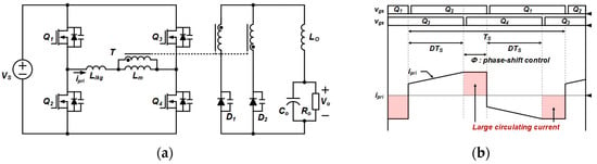
Figure 1.
Conventional phase-shifted full-bridge (PSFB) converter. (a) Circuit diagram. (b) Primary current waveform.

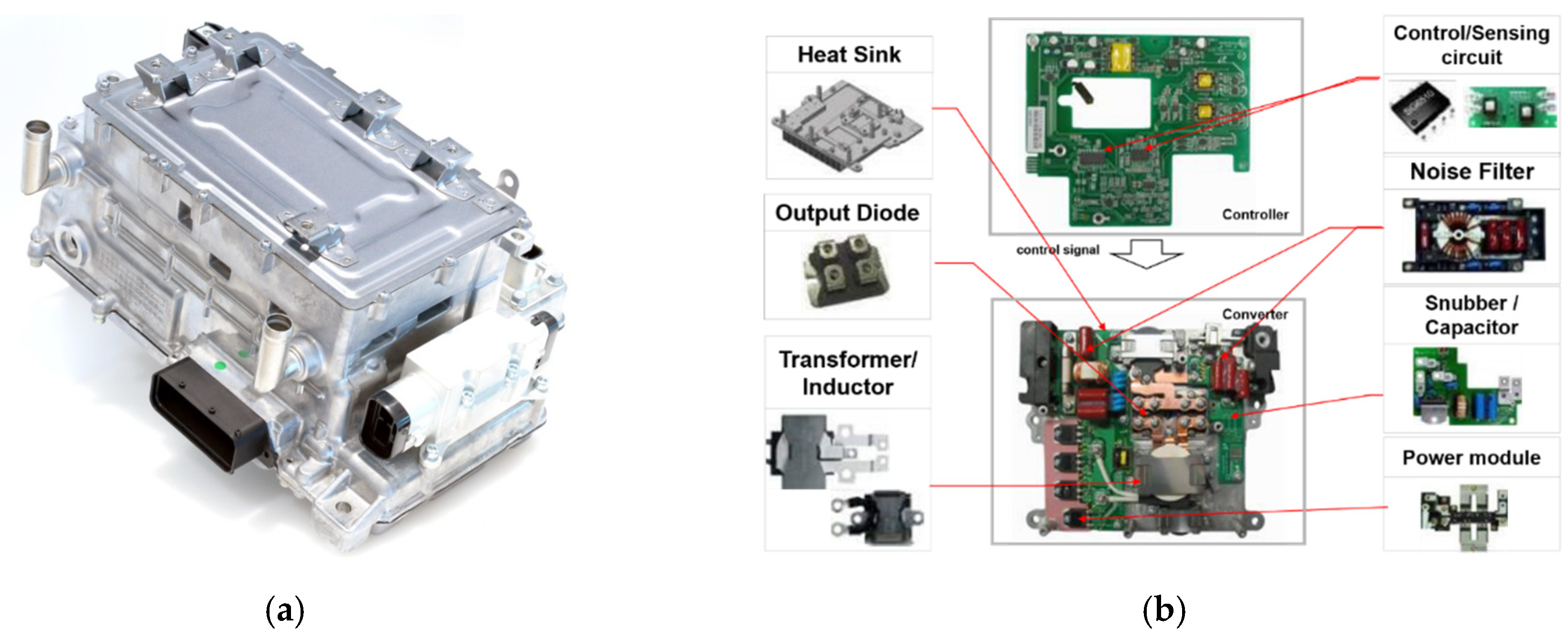
Figure 2.
Pictures of power control unit (PCU) and LDC converter for vehicle applications. (a) PCU. (b) LDC.
Many DC/DC topologies with low circulating current have been developed to reduce the conduction loss of the conventional PSFB converter [5,6,7,8,9,10,11]. The converter presented in [7] reduces the circulating current of the PSFB converter by using large resonant inductance. However, it has serious disadvantages of two additional switches and large volume of auxiliary inductor, which results in increasing the volume and cost of the LDC converter. The converters shown in [8,11] can obtain small circulating current by using an additional capacitor in the primary side or a coupled inductor in the secondary side. However, an additional capacitor in [8] cannot be small to handle high voltage stress and high current stress. A coupled inductor in [11] requires larger core size compared to a discrete output inductor to keep the same power loss. Moreover, these converters should have two separate magnetic components. Therefore, these converters are still limited in improving power density of the LDC converter.
To complement large circulating current of the conventional PSFB converter, many active-clamp-forward (ACF) converters have been studied [12,13,14,15,16,17,18,19]. These ACF converters have advantages of the zero circulating current and low number of switches, which results in lower conduction loss compared to the conventional PSFB converter. However, despite of low conduction loss, these converters suffer from high voltage stress on the primary switches, which becomes far worse taking into account wide input voltage range. As a result, the ACF converters in [12,13,14,15,16,17,18,19] should use low performance of Si-MOSFETs increasing conduction loss and switching loss. In order to improve this drawback and achieve high efficiency, the ACF converters can adopt silicon-carbide (SiC) MOSFETs which has high voltage rating, small on-resistance, and small parasitic capacitance. However, using SiC-MOSFETs significantly increases the cost of LDC converter. Moreover, the ACF converters still use two magnetic components increasing the volume of converter. To relieve the voltages stress on the primary switches of the ACF converters, three-switch ACF converters were researched and developed [14,15]. However, one of three switches still suffer from high voltage stress. Moreover, the converters in [14,15] should use complex driving circuits and two magnetic components. To reduce the number of the magnetic components, ACF converters with an integrated magnetic were represented as shown in Figure 3 [16,17]. Although these converters utilize only one integrated magnetic, the primary and secondary windings are wound the outside of the core shown in Figure 3, which requires additional shield and structure causing the extra cost and volume to minimize the adverse effect of electromagnetic interference (EMI). As a result, the conventional and previously studied ACF converters have limitations in commercialization especially for vehicle applications.
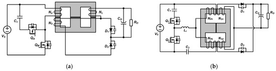
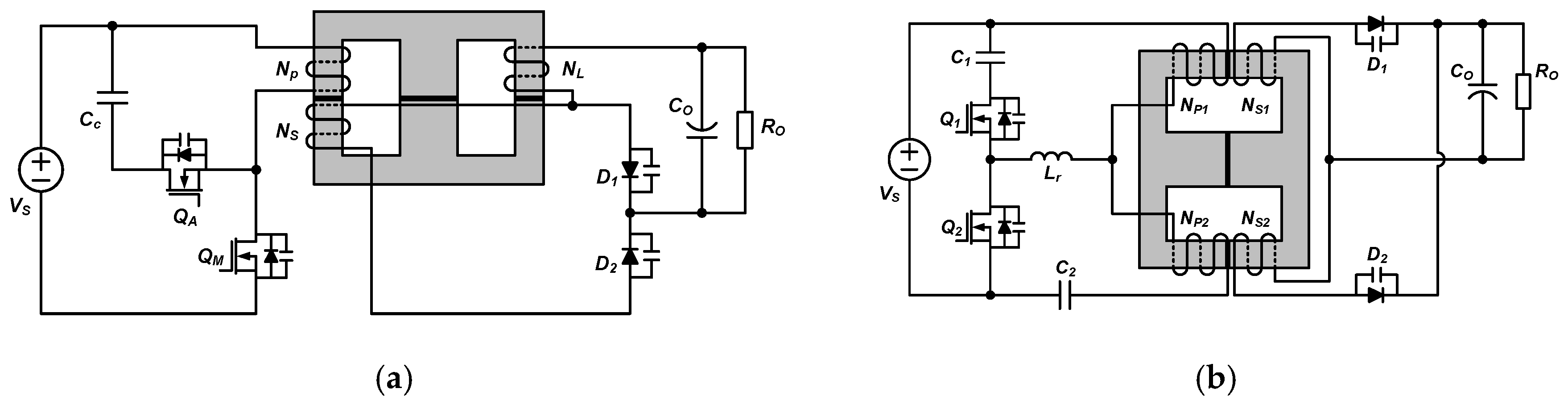
Figure 3.
Conventional active-clamp-forward (ACF) converters with integrated magnetics. (a) Integration of a transformer and an output inductor [16]. (b) Integration of two transformers [17].
In this paper, the full-bridge active-clamp-forward-flyback (FBACFF) converter adopting an integrated transformer sharing single primary winding is proposed for the LDC converter of vehicle applications. The proposed FACFF converter has the following advantages compared to conventional topologies: (1) active-clamp structure of the proposed converter minimizes the circulating current of the conventional PSFB converter, which results in higher efficiency; (2) full-bridge structure of the proposed converter relieves high voltage stress on the primary switches of the conventional ACF converter and thus the proposed converter can adopt cost-competitive Si-MOSFETs and achieve high efficiency without high-cost SiC-MOSFETs; (3) it can have lower diode voltage stress than the PSFB converter, which enables the proposed converter to use high-current rating diodes; and (4) a proposed single integrated transformer reduces volume and cost of the LDC converter. The primary and secondary windings of the proposed integrated transformer are wound inside of the transformer core, which enables the proposed converter not only to minimize the adverse effect of EMI but also to eliminate additional snubber circuits due to small leakage inductance. As a result, the proposed converter can achieve high efficiency, high power density, and low cost compared to the conventional topologies. In order to verify the validity of the proposed converter, a prototype with 200–310 V input and 1.8 kW (13.6 V/130 A) output was built and the experimental results are presented compared with the conventional PSFB converter which is the most widely used in the commercialized LDC converter.
2. Operational Principle
Figure 4 and Figure 5 show the circuit diagram and operational key waveforms of the proposed converter, respectively. In the proposed converter, the primary switches Q1 and Q4 are turned on at the same time to transfer the power from the input to the output through the forward transformer (Tfor). Meanwhile, the switches Q2 and Q3 are driven complementarily with Q1 and Q4 to reset Tfor as well as to deliver the energy stored in the flyback transformer (Tfly) into the output. For the sake of analysis, several assumptions are made as follows:
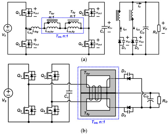
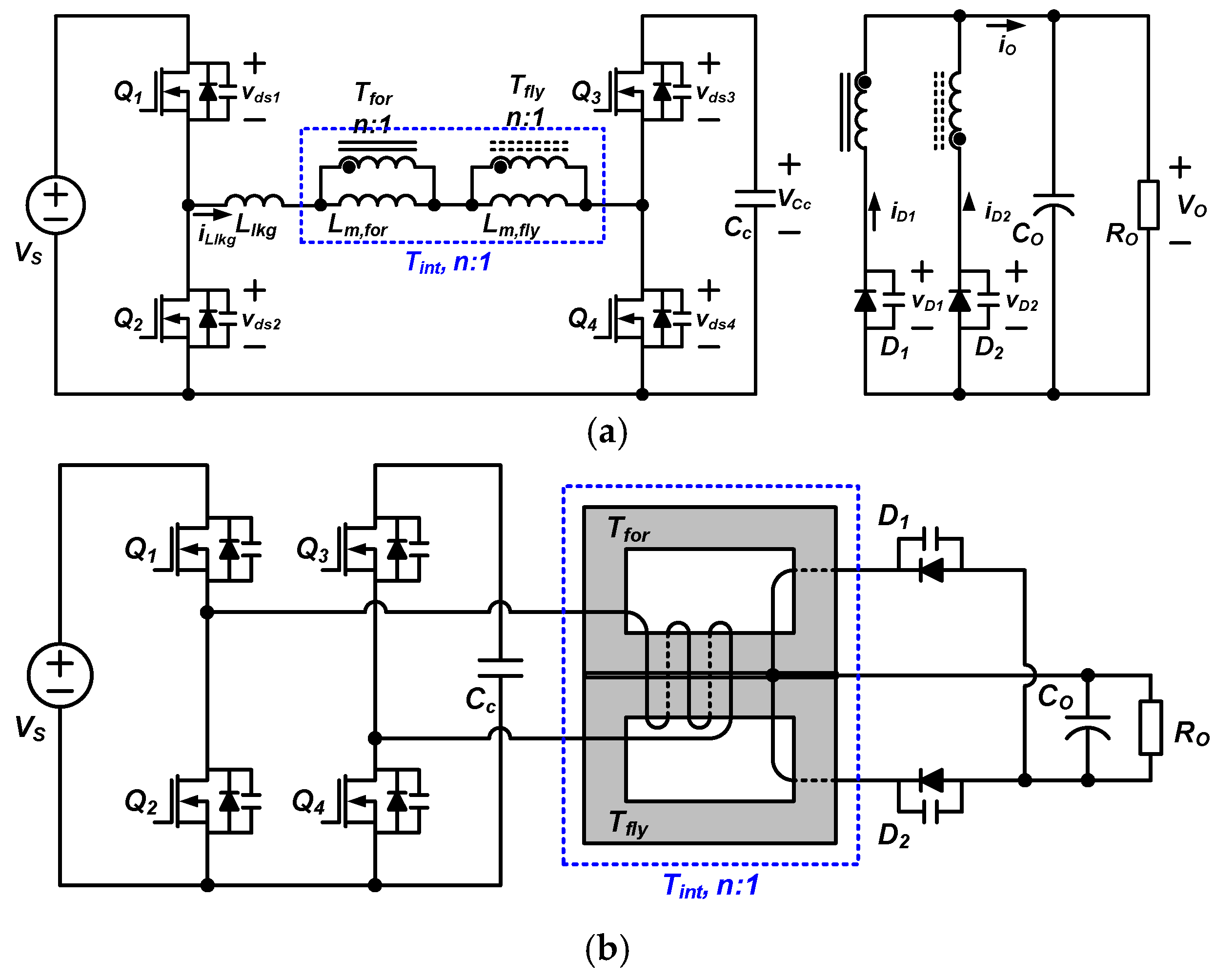
Figure 4.
Proposed converter. (a) Circuit diagram. (b) Circuit diagram with a proposed integrated transformer.
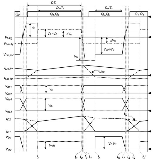
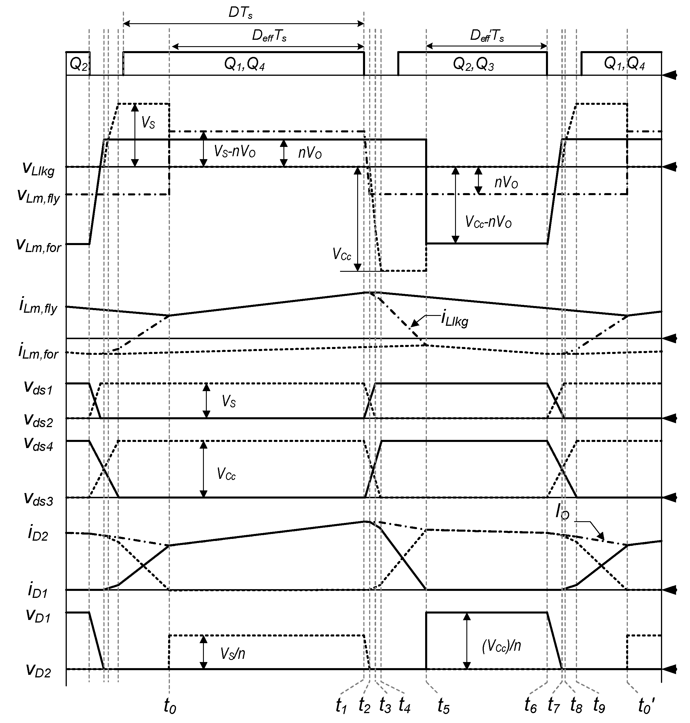
Figure 5.
Key operational waveforms of the proposed converter.
- (1)
- all parasitic components except for those specified in Figure 4 are ignored;
- (2)
- a clamp capacitor (CC) is large enough to be considered as a constant voltage source (VCc );
- (3)
- the output voltage (VO) is constant;
- (4)
- the transformer turns ratio (n) of the forward and flyback transformers (Tfor and Tfly) is N/1, where N is the number of the primary winding.
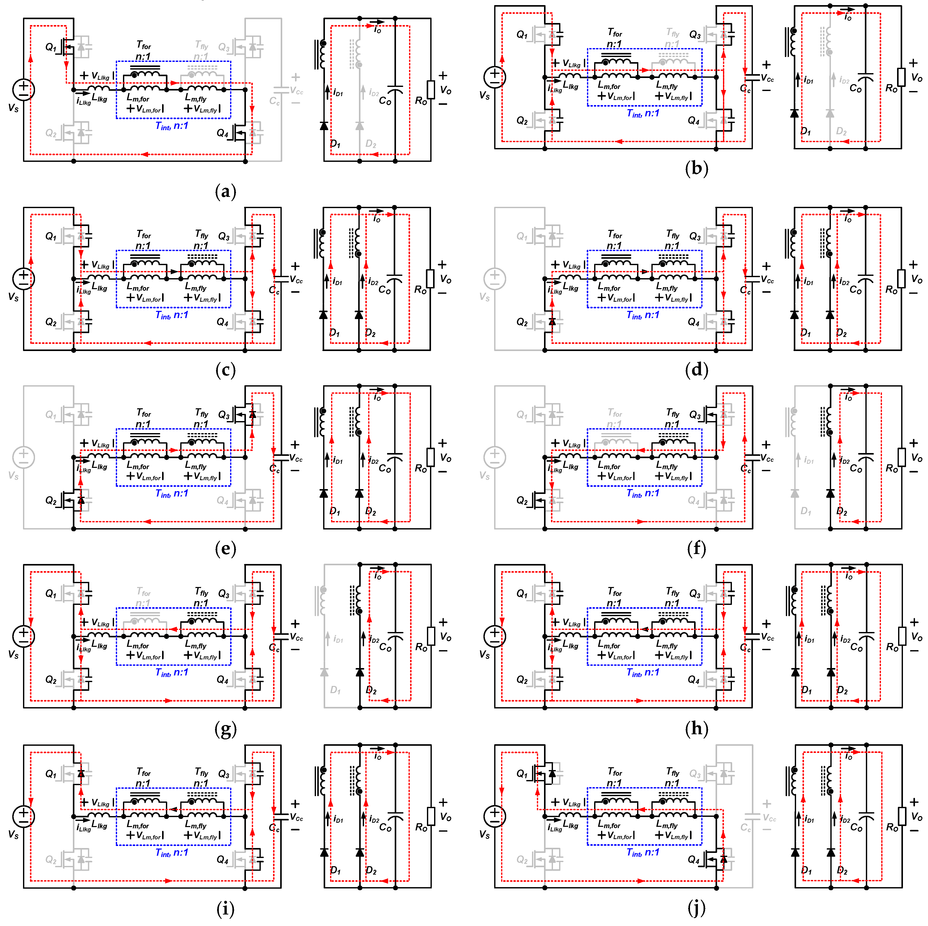
The proposed converter shows 10 operational modes during one switching period and each mode is explained with its topological state as shown in Figure 6.
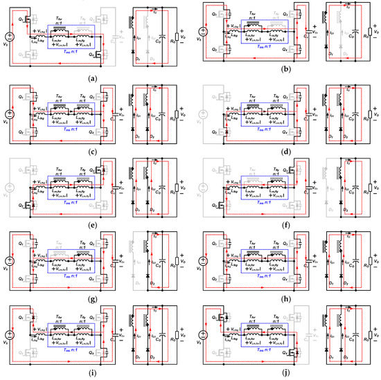
Figure 6.
Topological state of proposed converter. (a) Mode 1 (t0–t1). (b) Mode 2 (t1–t2). (c) Mode 3 (t2–t3). (d) Mode 4 (t3–t4). (e) Mode 5 (t4–t5). (f) Mode 6 (t5–t6). (g) Mode 7 (t6–t7). (h) Mode 8 (t7–t8). (i) Mode 9 (t8–t9). (j) Mode 10 (t9–t0’).
Mode 1 [t0–t1, Figure 6a]: At time t0, after the commutation of the secondary diodes (D1 and D2) ends and the leakage inductor current (iLlkg) reaches to the magnetizing current of Tfly (iLm,fly), nVO, and VS–nVO are applied to the magnetizing inductance of Tfor (Lm,for) and the magnetizing inductance of Tfly (Lm,fly), respectively. As a result, iLm,for, iLm,fly, and iLlkg are linearly increased. The power is transferred to the output through Q1, Q4, integrated transformer, and D1 at this mode. From the voltage across transformers, iLm,for, iLm,fly, and current of D1 (iD1) are expressed as follows:
Mode 2 [t1–t2, Figure 6b]: After t1, Q1 and Q4 are turned off, and mode 2 begins. iLm,fly is the same as the reflected load current (IO/n) charges Coss1 and Coss4 and discharges Coss2 and Coss3. Thus, the voltages across Q1 and Q4 (vds1 and vds4) simultaneously increase to VS/2, and the voltages across Q2 and Q3 (vds2 and vds3) decrease to VS/2 and VCc–VS/2, respectively. Thus, the voltage across Lm,fly (vLm,fly) is decreased from VS–nVO to –nVO so that the sum of the voltages across Lm,fly and Lm,for is zero at the end of this mode.
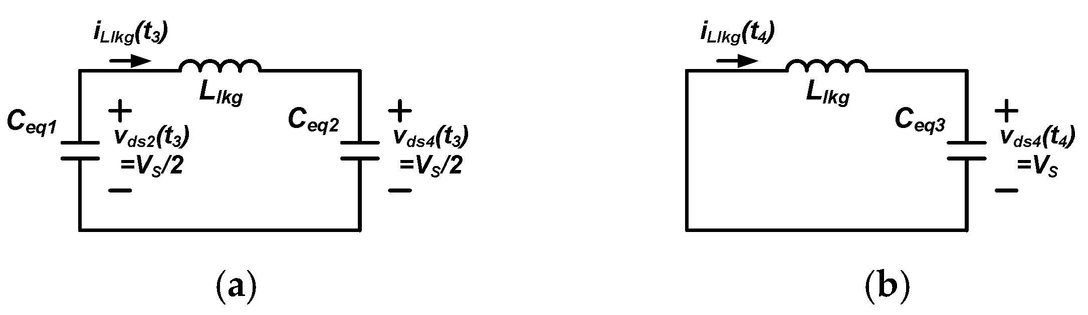
Mode 3 [t2–t3, Figure 6c]: vLm,fly reaches –nVO at t2, D1, and D2 start to conduct. The leakage inductance of the integrated transformer (Llkg) resonates with parasitic output capacitors (Coss1, Coss2, Coss3, and Coss4). The equivalent circuit of this mode is illustrated in Figure 7a. From this Figure, the energy stored in Llkg charges Coss1 and Coss4 and discharges Coss2 and Coss3. Thus, vds1 and vds4 are increased, and vds1 is clamped to VS. Meanwhile, vds2 and vds3 are decreased to zero and VCc–VS, respectively.

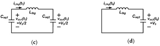
Figure 7.
Equivalent circuit of the proposed converter during switching transitions. (a) Mode 3 (t2–t3). (b) Mode 4 (t3–t4). (c) Mode 8 (t7–t8). (d) Mode 9 (t8–t9).
Mode 4 [t3–t4, Figure 6d]: After vds2 reaches to zero at t3, mode 4 starts. In this mode, only Coss3 and Coss4 are continuously discharged and charged by the resonance with Llkg, respectively. vds3 decreases to zero and vds4 increases to VCc. The equivalent circuit of this mode is depicted in Figure 7b. Based on Mode 3 and Mode 4, the ZVS condition of Q2 and Q3 are:
where Coss = Coss1 = Coss2 = Coss3 = Coss4.
Mode 5 [t4–t5, Figure 6e]: At time t4, vds2 and vds3 are 0 V, and iLkkg flows through body diodes of Q2 and Q3. As a result, Q2 and Q3 can achieve the ZVS operation. Moreover, since the sum of vLm.for and vLm.fly is zero, –VCc is applied to Llkg. Thus, iLlkg is linearly decreased to iLm.for with the commutation between D1 and D2. iLlkg at this mode is:
From (5), the commutation period, where the input power is not transferred to the output, can be approximated as LlkgIO/(nVCc).
Mode 6 [t5–t6, Figure 6f]: After the commutation of D1 and D2 ends, the voltage on D1 reaches VCc/n and the reset operation of Tfor starts by vLm,for (=nVO–VCc). Meanwhile, the energy stored in Tfly is delivered to the output because vLm,fly is –nVO. As a result, iLm,for, iLm,fly, and current of D2 (iD2) are expressed as follows:
Mode 7 [t6–t7, Figure 6g]: After t6, Q2 and Q3 are turned off, and mode 7 starts. iLm,for charges Coss2 and Coss3 and discharges Coss1 and Coss4. Thus, vds2 and vds3 are increased to VCc/2. vLm,for is increased from VCc–nVO to nVO. On the other hand, vds1 and vds4 are decreased to VS–VCc/2 and VCc/2, respectively. This mode ends when vLm,for reaches to nVO and the sum of the voltage on the magnetizing inductances is zero.
Mode 8 [t7–t8, Figure 6h]: vLm,for reaches nVO at t7 and D1 and D2 conduct. Thus, Llkg resonates with Coss1, Coss2, Coss3, and Coss4. The equivalent circuit of this mode is illustrated as in Figure 7. From this Figure, the energy stored in Llkg charges Coss2 and Coss3 and discharges Coss1 and Coss4. Thus, vds2 and vds3 are increased and vds2 is clamped to VS, whereas vds1 and vds4 are decreased to zero and VCc–VS, respectively.
Mode 9 [t8–t9, Figure 6i]: After vds1 reaches to zero at t8, Mode 9 begins. In this mode, only Coss3 and Coss4 are continuously charged and discharged in accordance with the resonance with Llkg. As a result, vds4 is decreased to zero and vds3 is increased to VCc. The equivalent circuit of this mode is depicted in Figure 7d. Based on Mode 8 and Mode 9, the ZVS condition of Q1 and Q4 is:
Mode 10 [t9–t0’, Figure 6j]: After vds1 and vds4 become 0 V, iLlkg flows through body diodes of Q1 and Q4. Thus, Q1 and Q4 can achieve the ZVS condition. Moreover, similar to Mode 5, since the sum of vLm.for and vLm.fly is zero, VS is applied to the Llkg. Thus, iLlkg is linearly increased to iLm.flly with the commutation between D1 and D2. iLlkg at this mode is:
From (10), the commutation period can be derived as LlkgIO/(nVS).
3. Analysis and Design Consideration
In this chapter, characteristics of the proposed converter are analyzed. Moreover, the design consideration of the proposed integrated transformer will be discussed to achieve high power density and simple secondary structure of the proposed converter.
3.1. DC Conversion Ratio
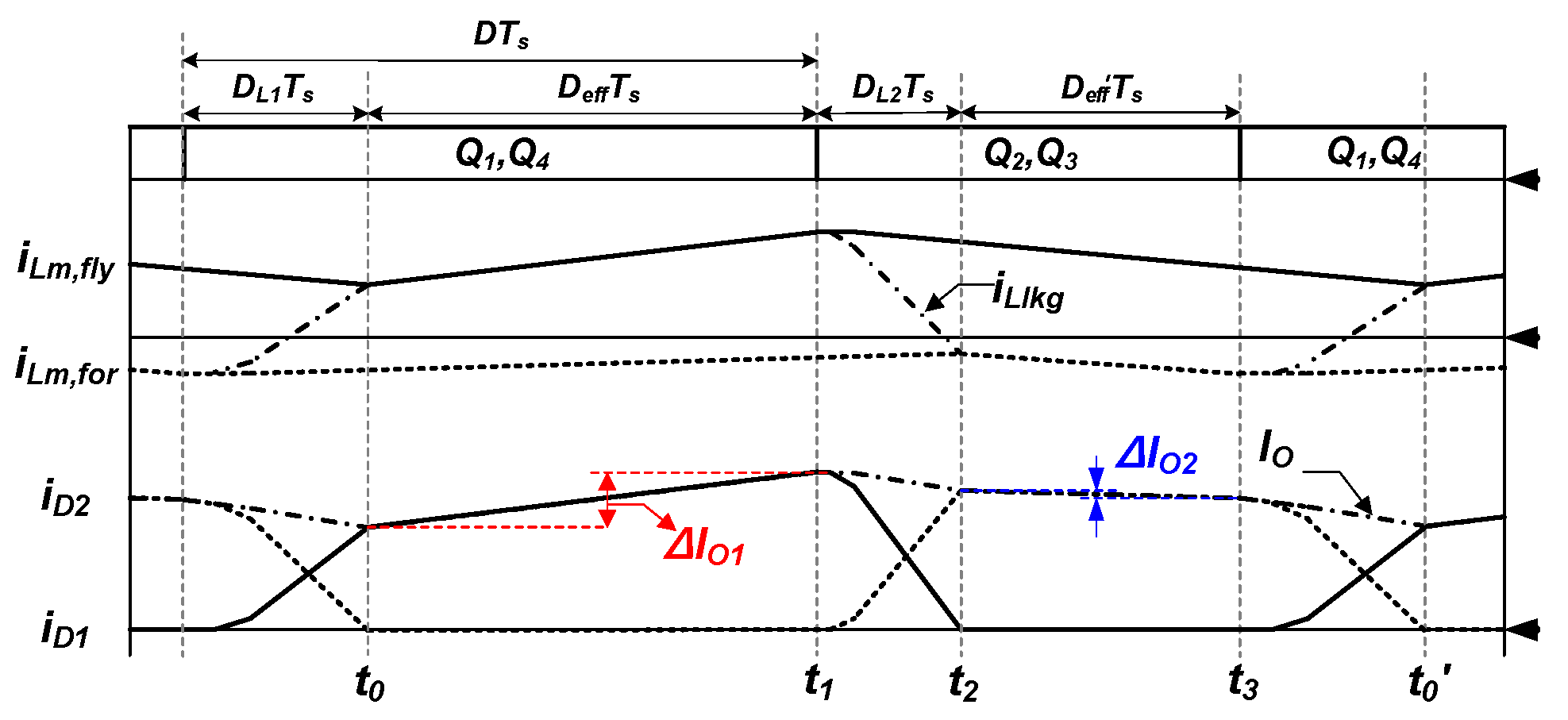
For simplifying analysis of the proposed converter, Llkg and the dead time among Q1–Q4 are ignored. In Figure 8, VS–nVO and –nVO are applied to the Lm,fly during DTS and (1–D)TS, respectively. Thus, the DC conversion ratio can be approximated as in (12) by the voltage second balance of Lm,fly.
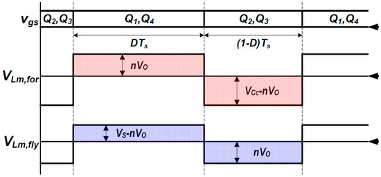
Figure 8.
Applied voltage on Lm,for and Lm,fly of the proposed converter.
Moreover, based on the voltage second balance of Lm,for and Figure 8, VCc can be achieved as follows:
From Figure 9, the DC conversion ratio and VCc can be recalculated by considering the duty loss1 (DL1) caused by the commutation operation when the Q1 and Q4 are turned on, the duty loss2 (DL2) resulting from the commutation operation at the Q2 and Q3 turn-on instant as follows:
where IO is the output load current, fS is the switching frequency, DL1 is LlkgIOfS/nVS, and DL2 is LlkgIOfS/nVCc.
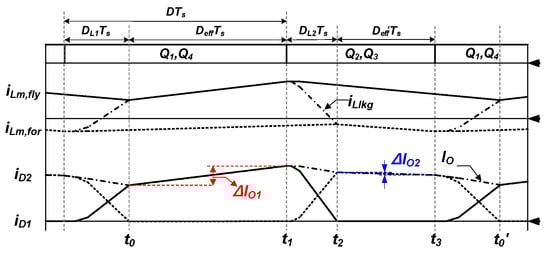
Figure 9.
Primary and secondary current waveforms of proposed converter neglecting the dead-time.
Therefore, the DC conversion ratio of the proposed converter is almost the same as that of the conventional ACF converter.
3.2. Output Current Ripple
The conventional isolated converters, such as PSFB and ACF converters, generally adopt two magnetics: (1) transformer to transfer power from the input to the output and (2) output inductor to control the output current ripple and output voltage ripple. Meanwhile, one integrated transformer of the proposed converter can play role as two traditional magnetics. Tfor of the integrated transformer operates as the transformer of the conventional isolated converter and Tfly plays role as the output inductor of the conventional converters. In addition, as shown in Figure 9, the difference of iLm.for and iLm.fly is reflected to the output current. As a result, the magnitude of Lm,for and Lm,fly determines the output current ripple and output voltage ripple. From Figure 9, the output current ripples can be represented as in (17) and (18). The maximum output current ripple can be decided on the larger value between (17) and (18):
where k = Lm,for/(Lm,for + Llkg).
Therefore, Lm,fly and Lm,for of the integrated transformer in the proposed converter should be adequately designed and chosen to satisfy the requirement of the output current and voltage ripples.
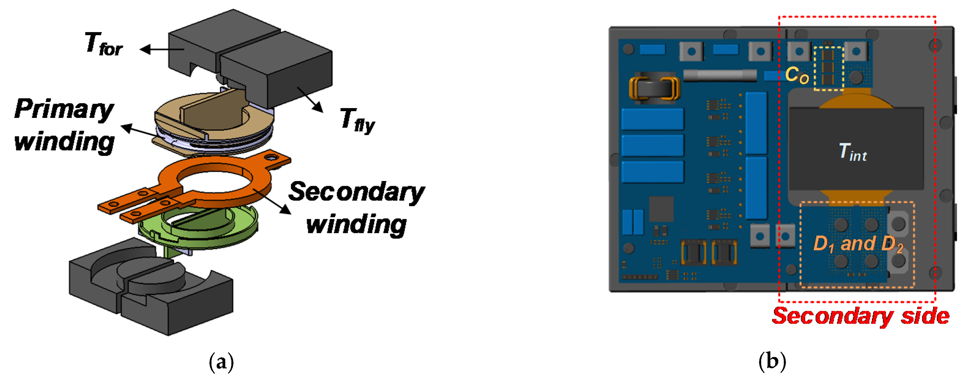
3.3. Transformer Design and Core Loss
The proposed converter with the integrated transformer shown in Figure 10 can minimize the number of the magnetic components through the integration of Tfor and Tfly. Moreover, the integrated transformer enables the proposed converter to simplify the secondary side without snubber circuits for the secondary diodes. To implement an integrated transformer, various research and studies have been conducted [16,17]. However, these methods have several disadvantages such as large conduction losses due to separate primary and secondary windings and EMI problem caused by the windings wound outside the core, which requires additional bulky and expensive shield to reduce the adverse effect of the EMI.

Figure 10.
Integrated transformer of the proposed converter. (a) Structure of the integrated transformer. (b) Concise secondary side structure.
In this paper, by using a characteristic that the primary currents of the forward and flyback transformers are the same, an integrated transformer for Tfor and Tfly is proposed where two cores are separate and share the primary winding. In Figure 10, both the primary winding and secondary busbar are wound inside the core. As a result, the proposed integrated transformer can reduce the length of the transformer windings than those of the conventional integrated transformers in [16,17], which results in lower conduction loss of the transformer. Moreover, due to the windings wound inside the core, the proposed integrated transformer can have better EMI characteristics than the conventional integrated transformers [16,17]. Therefore, no additional shield is required in the proposed converter. In addition, as shown in Figure 10b, it is noted that the proposed converter can significantly simplify the secondary rectifier structure because the secondary busbar is directly connected to the output capacitor, which results in higher power density. Furthermore, there is no flux interference because two cores are separate from each other.
The flux density of the proposed integrated transformer can be simply calculated by considering its operation. When Q1 and Q4 are turned on, D1 conducts and the power is transferred to the output through Tfor. At that time, Tfly stores energy since D2 is reverse biased and there is no current on Tfly and D2. Whereas, when Q2 and Q3 are turned on, D2 conducts. Thus, the energy stored in Tfly starts to be transferred to the output through Tfly and D2, while Tfor is reset by VCc. During these two periods, the flux variations of both cores (Tfor and Tfly) can be expressed as follows:
where NP is the number of primary windings of the integrated transformer and Ae,for and Ae,fly are the effective cross-section area of each core.
To analyze the core loss of the proposed integrated transformer, the improved generalized Steinmetz equation (IGSE) can be adopted because the flux variations of both cores are not sinusoidal. The transformer core loss based on the IGSE can be expressed as follows:
where ΔB is the peak-to-peak flux variation, and
where parameters k, α, and β are the same parameters as used in the Steinmetz equation [20].
Assuming that the transformer turns the ratio of the proposed and conventional integrated transformers the same way, the core loss of the proposed integrated transformer is the same as that of the conventional integrated transformer for the ACF converters. Meanwhile, the proposed integrated transformer can have slightly larger core loss than the conventional PSFB converter with a transformer and output inductor. This is because the turns-ratio of the proposed integrated transformer is restricted due to the shared primary windings. Thus, the number of primary windings of the proposed integrated transformer can be lower than that of the transformer and output inductor in the conventional PSFB converter, which can increase the core loss of the proposed converter compared to the conventional PSFB converter. Since ΔIO is determined by the Lm,for and Lm,fly, relatively small Lm,for and Lm,fly should be designed to satisfy the requirement of ΔIO. Due to the relatively larger core loss and magnetizing current, the proposed converter may have lower light load efficiency than the conventional PSFB converter. On the other hand, the proposed integrated transformer results in high heavy load efficiency because single primary windings and optimized busbar structure decrease the conduction loss caused by the output current. As mentioned in introduction section, the importance of heavy load efficiency in eco-friendly vehicles has been increasing more than before as the electric load of the vehicle has considerably increased. Therefore, the proposed integrated transformer is appropriate for the LDC converter of eco-friendly vehicles. Furthermore, the proposed integrated transformer not only reduces the volume of the converter but also achieves a high price competitiveness due to the concise secondary rectifier structure as shown in Figure 10b.
3.4. Conduction Loss and Voltage Stresses on Switches and Diodes
For the sake of analysis, it is assumed that (1) Lm,for and Lm,fly are large enough to ignore the effect of the magnetizing current during a switching period and (2) Llkg is small enough to neglect the effect of the commutation period. Based on this assumption, RMS currents and voltage stress on the primary switches and secondary diodes can be derived for the conventional PSFB converter, conventional ACF converter, and proposed converter (Table 1). From Table 1, it can be seen that the proposed converter has negligible RMS currents on Q2 and Q3, inducing the ignorable conduction loss. Thus, the conduction loss on primary switches is much smaller than that of the conventional PSFB converter and this tendency becomes larger as the output current goes to heavier load condition.

Table 1.
Components stresses comparison among the conventional and proposed converters.
Due to the full-bridge active clamp structure, the proposed converter can achieve lower maximum voltage stresses on primary switches (Q1 and Q2: 310 V, Q3 and Q4: 238.6 V under experimental conditions) compared to the conventional ACF converter (Qmain and Qaux: 477.7 V). Thus, considering a 30% voltage margin, the proposed converter can adopt Si-MOSFETs with low cost and low on-resistance rather than SiC-MOSFETs having high cost and high voltage rating characteristics (Table 2). Moreover, the proposed converter reduces the maximum voltage stresses on D1 and D2 (D1: 29.8 V, D2: 38.8 V without considering voltage ringing under experimental conditions) than the conventional PSFB converter (D1 and D2: 62 V). Therefore, the proposed converter can utilize low voltage and high current rating diodes without bulky and lossy snubber circuit.
Table 2.
Price comparison of the primary switches among the conventional and proposed converters.
4. Experimental Results
To prove the validity of the proposed converter, a 1.8 kW prototype shown in Figure 11a was built with the specification of VS = 200–310 V, VO = 13.6 V, fS = 125 kHz at 200 V input – 150 kHz at 310 V input. We also implemented a conventional PSFB converter. Table 3 summarizes the details of two prototypes. In this chapter, the commercialized PSFB converter was designed for IONIQ HEV (made by HYUHNDAI motor company) and is used as the conventional converter to compare the performance of the proposed converter.
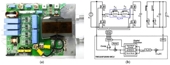
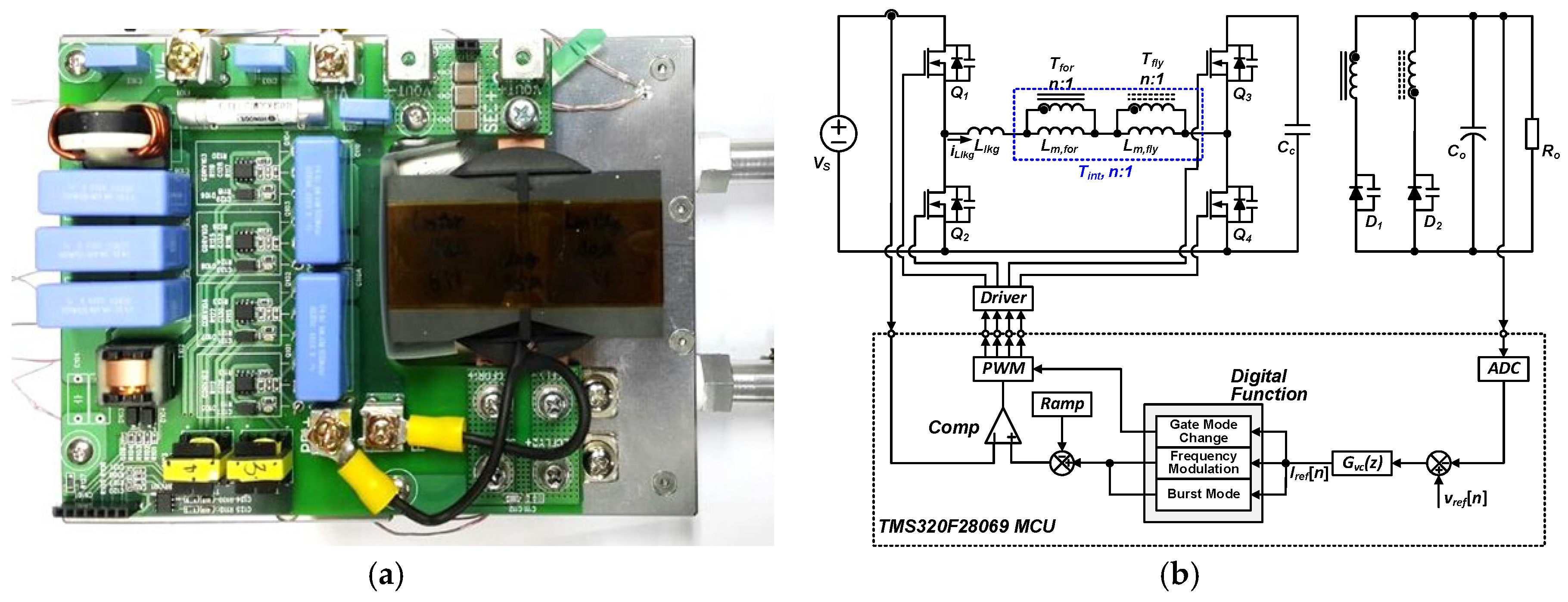
Figure 11.
Prototype and control block diagram of proposed converter. (a) Prototype. (b) Control block diagram.
Table 3.
Design Parameters.
To regulate the output voltage, as shown in Figure 11b, the proposed converter used a DSP that is TMS320F28069PZT with 90 MHz clock frequency and 12-bit analog to digital conversion module. The DSP is used to implement the output voltage control and the switching frequency variation. The duty to output voltage transfer function of the proposed converter can be derived like a buck converter as follows:
where γ is 1 + Lm,fly/Lm,for.
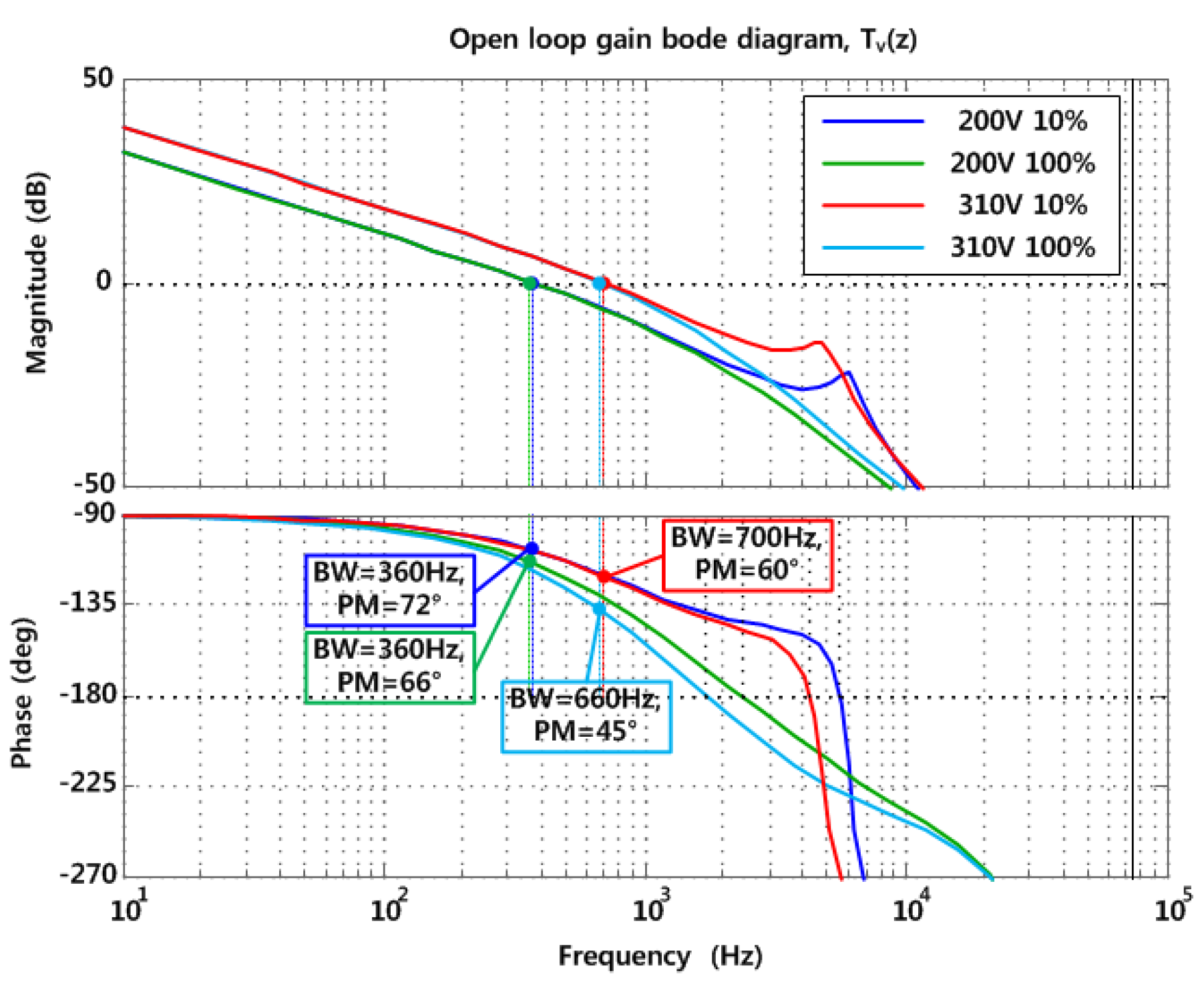
The loop gain (Tv(z)) of the proposed converter adopting the voltage compensator is illustrated in Figure 12. The voltage compensator (Gvc(z)) was designed for minimum 360 Hz bandwidth and 45° phase margin for the prototype of this paper.
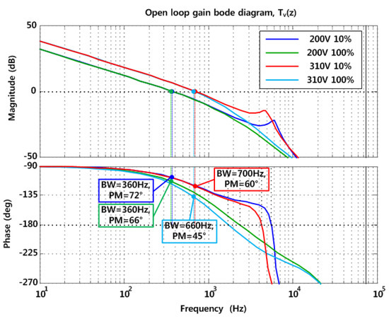
Figure 12.
Loop gain of the proposed converter with voltage compensator.
In addition, since the DSP is placed in the secondary side, the pulse transformer which can transfer gate signals from the secondary side to the primary side is implemented. In addition, for measuring the performance of the conventional and proposed converters, NFES2000S is used as an input power supply, Chroma DC Electronic load 63203 as an output electronic load, YOKOGAWA WT1600 as an input power analyzer, FLUKE 45A digital multi-meter for the output voltage and current measuring, and Wave-runner 64xi TELEDYNE LECROY to capture the experimental waveforms.
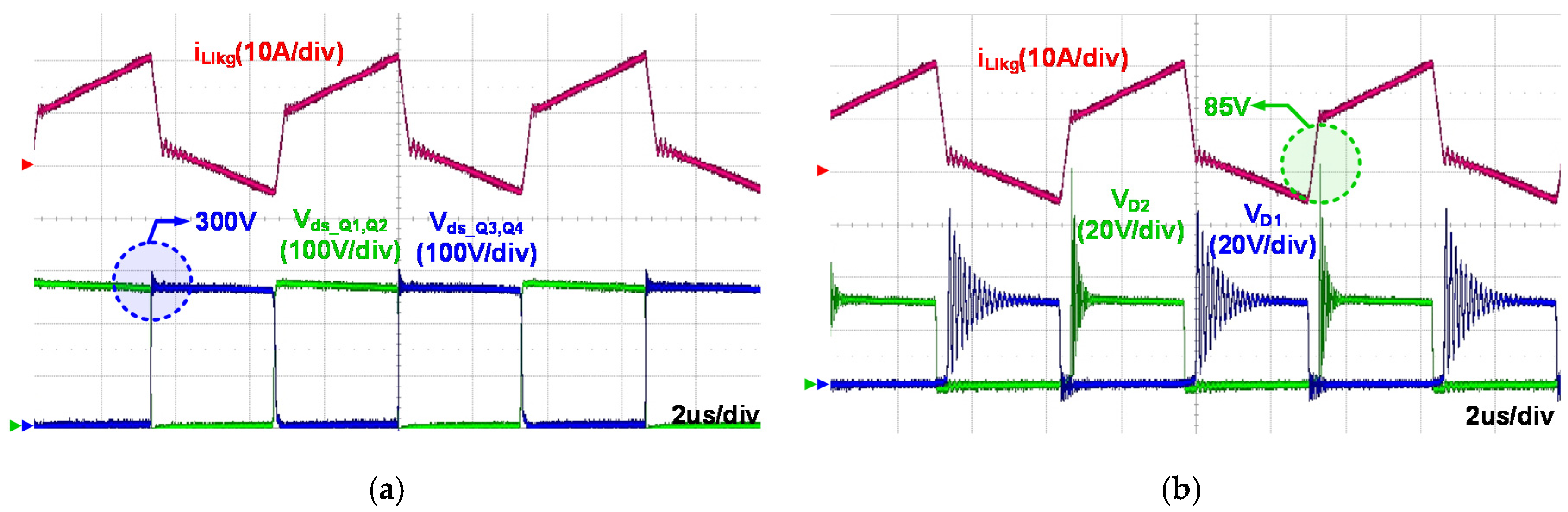
Figure 13 shows the experimental waveforms of the proposed converter at the nominal input voltage (VS = 270 V) and full-load condition with the 150 kHz switching frequency. As shown in Figure 13a, due to the ACF structure, there is no circulating current and only small commutation current occurs during the switch transition. Moreover, voltage stresses on the primary switches of the proposed converter is far lower than 650 V which is general breakdown voltage of high-performance Si-MOSFETs. As a result, the primary conduction loss of the proposed converter can be considerably reduced compared to the conventional PSFB converter. Moreover, the propose converter cuts the production cost by utilizing Si-MOSFETs and the integrated transformer with single and inside wounded primary and secondary windings.
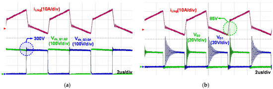
Figure 13.
Key experimental waveforms at 270 V input and 100% load conditions (D = 0.605). (a) Primary side key experimental waveforms. (b) Secondary side key experimental waveforms.
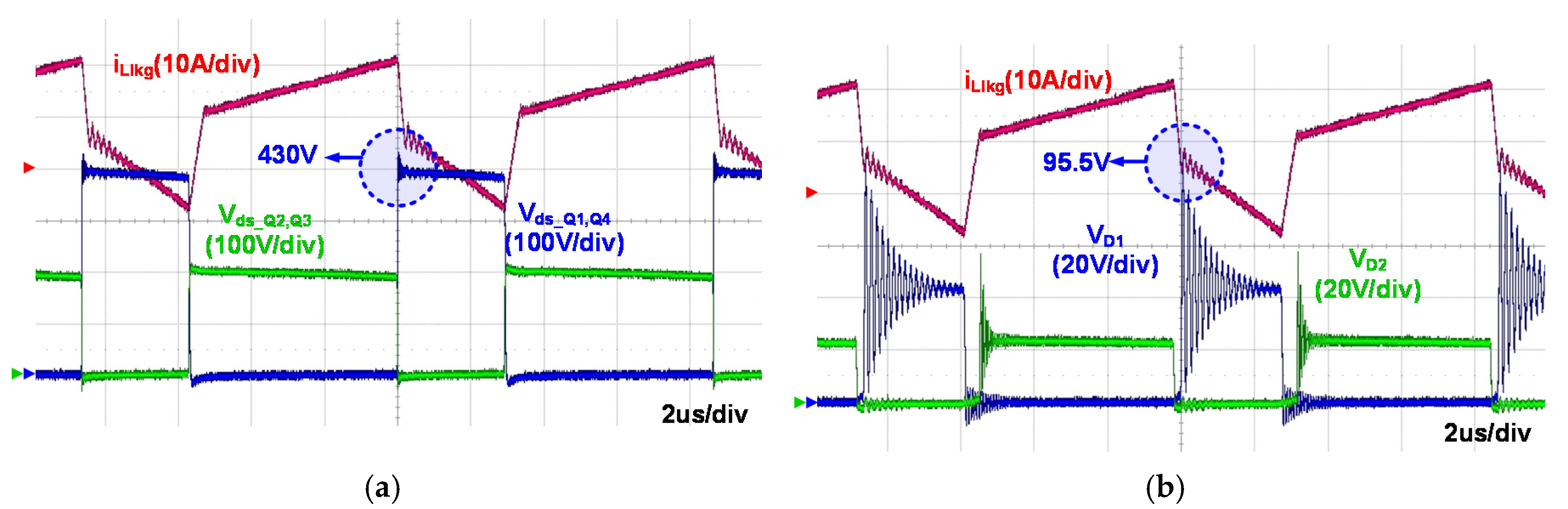
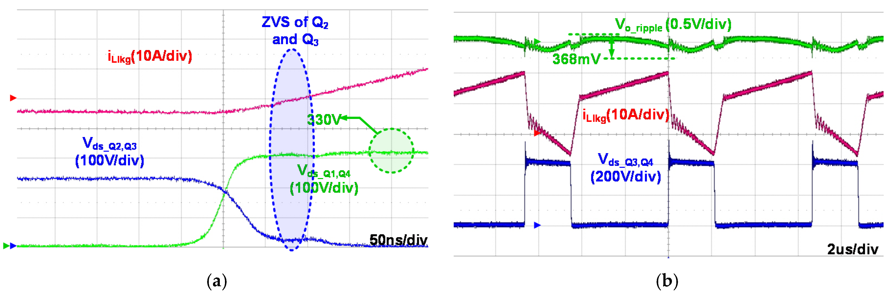
Figure 14 and Figure 15 present the key experimental waveforms at the minimum and maximum input voltage conditions under the full load condition. As shown in Figure 14, in the minimum input voltage condition (VS = 200 V), since the maximum switch voltage stresses are determined by the actual duty ratio that is sum of the effective duty ratio and the duty loss during the commutation period, the switching frequency varies from 150 kHz to 125 kHz at the minimum input voltage condition to reduce the ratio of the commutation period in the total switching period. As a result, the voltage stresses on the primary switches are well restricted near 400 V, and the secondary diode voltage stresses are under 100 V. Since the duty ratio (D) of the proposed converter can be designed to be over 0.5, the proposed converter well regulates the output voltage at the minimum input voltage condition with D = 0.605. Moreover, as can be seen in Figure 15, the voltage stresses on the switches and diodes are under 400 V and 100 V in the maximum input voltage condition (VS = 310 V). Although the voltage stresses on the switches and diodes varies according to the input voltage conditions, all of them are well controlled and restricted to be suitable for high performance Si-MOSFET with low cost and low on-resistance. Furthermore, the ZVS operation of the proposed converter is achieved even in the worst-case condition such as the high input voltage and full-load conditions shown in Figure 16a. Figure 16b shows the output voltage ripple of the proposed converter. The maximum output voltage ripple is under 500 mV regardless of the input voltage and load conditions (500 mV is the output voltage ripple requirement of LDC converter for vehicle applications). This verifies that the magnetizing inductances of the proposed integrated transformer is adequately designed and chosen. Thus, despite the integrated transformer, the proposed converter can effectively constrain the output current ripple.
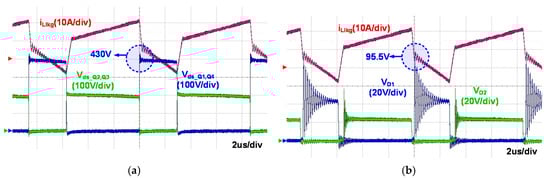
Figure 14.
Key experimental waveforms at 200 V input and 100% load conditions (D = 0.464). (a) Primary side key experimental waveforms. (b) Secondary side key experimental waveforms.
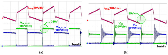
Figure 15.
Key experimental waveforms at 310 V input and 100% load conditions (D = 0.412). (a) Primary side key experimental waveforms. (b) Secondary side key experimental waveforms.
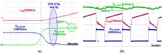
Figure 16.
ZVS and output voltage ripple waveforms at worst case conditions. (a) ZVS waveforms at 310 V input and 100% load conditions. (b) Output voltage ripple waveforms at 200 V input and 100% load conditions.
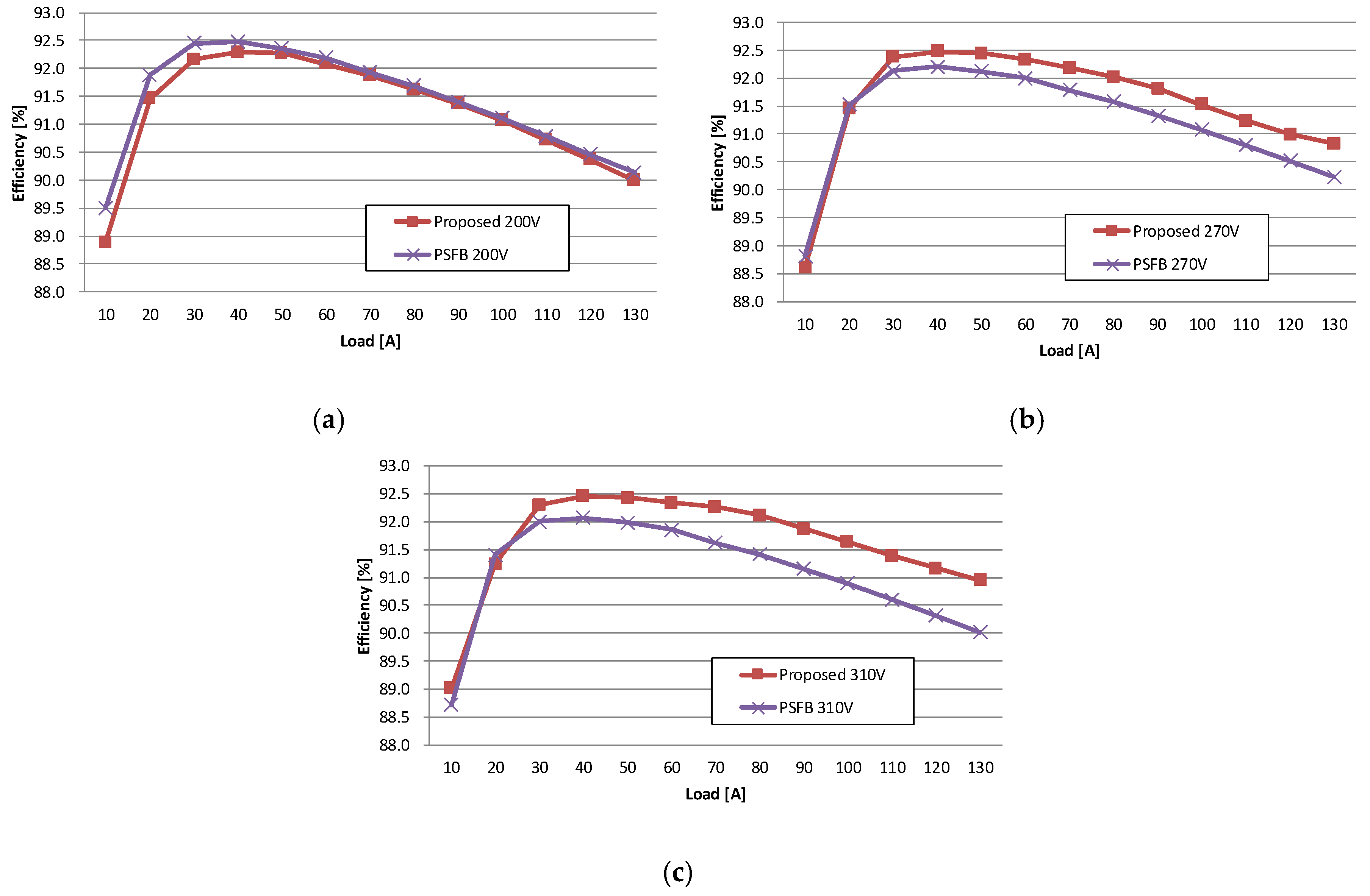
Figure 17 shows the measured efficiency of the proposed and conventional PSFB converters. In the minimum input voltage condition, the efficiency of the proposed converter is almost the same as that of PSFB converter because the PSFB converter operates with a duty ratio near 0.5. Meanwhile, in the nominal and maximum input voltage conditions, as previously analyzed, the proposed converter shows higher efficiency over the 30% load conditions due to the reduced circulating and conduction loss of the Q2 and Q3 switches. On the other hand, because of large core loss and small magnetizing inductances of the integrated transformer, the efficiency of the proposed converter is similar to that of the conventional PSFB converter under light load condition. However, since the importance of the high heavy load efficiency is gradually increased, the proposed converter is attractive for the LDC converter of the vehicle applications. Moreover, the proposed converter is a very promising converter for other wide input and high output power applications due to its high efficiency and high power density characteristics.
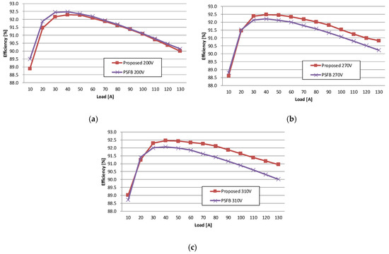
Figure 17.
Measured efficiency according to input voltage. (a) Minimum input (VS = 200 V, D = 0.605). (b) Nominal input (VS = 270 V, D = 0.464). (c) Maximum input (VS = 310 V, D = 0.412).
5. Conclusions
In this paper, a novel FBACFF converter with an integrated transformer sharing primary windings is proposed to achieve high efficiency and high power density LDC converter for vehicle applications. The operation principles and features are analyzed and illustrated, and the effectiveness of the proposed converter is verified by the experimental results with 13.6 V and 1.8 kW prototype. In the proposed converter, due to the full-bridge active-clamp structure, the proposed converter can reduce the primary conduction loss by eliminating the circulating current and utilize low cost Si-MOSFETs by relieving burden of the primary voltage stress. In addition, the proposed converter can improve power density through the integrated transformer with the shared and wounded inside windings. Furthermore, the secondary side structure can be simplified and optimized. Based on these advantages, the proposed converter can achieve not only high efficiency and high power density but also low cost. Therefore, the proposed converter is expected to be widely adopted for applications with wide input voltage range and high output current such as the LDC converter for vehicle applications. The efficiency and power density of the proposed converter can be much improved with planar transformer and synchronous rectification techniques.
Author Contributions
J.B. and H.-S.Y. were the main researchers who initiated and organized research reported in the paper. All authors including H.-S.Y. were responsible for making the prototype of the proposed system and carrying out the experiment. All authors have read and agreed to the published version of the manuscript.
Funding
This work was supported by Incheon National University (International Cooperative) Research Grant in 2019.
Conflicts of Interest
The authors declare not conflict of interest.
References
- Greenhouse Gas Emissions from a Typical Passenger Vehicle. Available online: https://www.epa.gov-/greenvehicles/greenhouse-gas-emissions-typical-passenger-vehicle (accessed on 31 March 2018).
- CO2 Emission Standards for Passenger Cars and Light-Commercial Vehicles in the European Union. Available online: https://theicct.org/publications/ldv-co2-stds-eu-2030-update-jan2019 (accessed on 31 January 2019).
- Global EV Outlook 2019. May 2019. Available online: https://www.iea.org/reports/global-ev-outlook-2019 (accessed on 15 February 2020).
- Evolution of Vehicle Architecture. Available online: https://www.aptiv.com/newsroom-/article/evolution-of-vehicle-architecture (accessed on 30 June 2018).
- Li, W.; Li, P.; Yang, H.; He, X. Three-level forward–flyback phase-shift ZVS converter with integrated series-connected coupled inductors. IEEE Trans. Power Electron. 2012, 27, 2846–2856. [Google Scholar] [CrossRef]
- Gu, B.; Lin, C.-Y.; Chen, B.; Dominic, J.; Lai, J.-S. Zero-VoltageSwitching PWM resonant full-bridge converter with minimized circulating losses and minimal voltage stresses of bridge rectifiers for electric vehicle battery chargers. IEEE Trans. Power Electron. 2013, 28, 4657–4667. [Google Scholar] [CrossRef]
- Kim, Y.-D.; Cho, K.-M.; Kim, D.-Y.; Moon, G.-W. Wide-Range ZVS phase-shift full-bridge converter with reduced conduction loss caused by circulating current. IEEE Trans. Power Electron. 2013, 28, 3308–3316. [Google Scholar] [CrossRef]
- Kim, Y.-D.; Lee, I.-O.; Cho, I.-H.; Moon, G.-W. Hybrid dual full-bridge DC–DC converter with reduced circulating current, output filter, and conduction loss of rectifier stage for RF power generator application. IEEE Trans. Power Electron. 2014, 29, 1069–1081. [Google Scholar]
- Safaee, A.; Jain, P.; Bakhshai, A. A ZVS pulse width modulation full bridge converter with a low-RMS-current resonant auxiliary circuit. IEEE Trans. Power Electron. 2016, 31, 4031–4047. [Google Scholar] [CrossRef]
- Zhao, L.; Li, H.; Wu, X.; Zhang, J. An improved phase-shifted full-bridge converter with wide-range ZVS and reduced filter requirement. IEEE Trans. Ind. Electron. 2018, 65, 2167–2176. [Google Scholar] [CrossRef]
- Han, J.K.; Moon, G.W. High-Efficiency Phase-Shifted Full-Bridge Converter with a New Coupled Inductor Rectifier (CIR). IEEE Trans. Power Electron. 2019, 34, 8468–8480. [Google Scholar] [CrossRef]
- Zhang, F.; Yan, Y. Novel forward-flyback hybrid bidirectional DC-DC converter. IEEE Trans. Ind. Electron. 2009, 56, 1578–1584. [Google Scholar] [CrossRef]
- Park, K.B.; Kim, C.E.; Moon, G.W.; Youn, M.J. Three-switch active-clamp forward converter with low switch voltage stress and wide ZVS range for high-input-voltage applications. IEEE Trans. Power Electron. 2010, 25, 889–898. [Google Scholar] [CrossRef]
- Kim, C.E.; Baek, J.I.; Lee, J.B. Improved Three Switch-Active Clamp Forward Converter with Low Switching and Conduction Losses. IEEE Trans. Power Electron. 2019, 34, 5209–5216. [Google Scholar] [CrossRef]
- Moon, S.; Park, K.B.; Moon, G.W.; Youn, M.J. Analysis and design of active clamp forward DC to DC converter with asymmetric two transformers. In Proceedings of the 8th International conference on power electronics ECCE Asia, Jeju, South Korea, 30 May–3 June 2011; pp. 599–606. [Google Scholar]
- Chen, Q.; Feng, Y.; Zhou, L.; Wang, J.; Ruan, X. An improved active clamp forward converter with integrated magnetics. In Proceedings of the IEEE Power Electronics Specialists Conference(PESC), Orlando, FL, USA, 17–21 June 2007; pp. 377–382. [Google Scholar]
- Lin, J.-Y.; Lo, Y.-K.; Chiu, H.-J.; Wang, C.-F.; Lin, C.-Y. An active-clamping ZVS flyback converter with integrated transformer. In Proceedings of the 2014 International Power Electronics Conference (IPEC-Hiroshima 2014—ECCE ASIA), Hiroshima, Japan, 18–21 May 2014; pp. 172–176. [Google Scholar]
- Lee, J.-H.; Park, J.-H.; Jeon, H. Series-connected forward-flyback converter for high step-up power conversion. IEEE Trans. Power Electron. 2011, 26, 3629–3641. [Google Scholar] [CrossRef]
- Lee, H.S.; Choe, H.J.; Ham, S.H.; Kang, B. High-efficiency asymmetric forward-flyback converter for wide output power range. IEEE Trans. Power Electron. 2017, 32, 433–440. [Google Scholar] [CrossRef]
- Reinert, J.; Brockmeyer, A.; de Doncker, R. Calculation of losses in ferro- and ferrimagnetic materials based on the modified Steinmetz equation. IEEE Trans. Ind. Appl. 2001, 37, 1055–1061. [Google Scholar] [CrossRef]


© 2020 by the authors. Licensee MDPI, Basel, Switzerland. This article is an open access article distributed under the terms and conditions of the Creative Commons Attribution (CC BY) license (http://creativecommons.org/licenses/by/4.0/).