Abstract
In this paper, the relationship between coordination complexes and electrical properties according to the bonding structure of boron and silicon was analyzed to optimize the p–n junction quality for high-efficiency n-type crystalline solar cells. The p+ emitter layer was formed using boron tribromide (BBr3). The etch-back process was carried out with HF-HNO3-CH3COOH solution to vary the sheet resistance (Rsheet). The correlation between boron–silicon bonding in coordination complexes and electrical properties according to the Rsheet was analyzed. Changes in the boron coordination complex and boron–oxygen (B–O) bonding in the p+ diffused layer were measured through X-ray photoelectron spectroscopy (XPS). The correlation between electrical properties, such as minority carrier lifetime (τeff), implied open-circuit voltage (iVoc) and saturation current density (J0), according to the change in element bonding, was analyzed. For the interstitial defect, the boron ratio was over 1.8 and the iVoc exceeded 660 mV. Additional gains of 670 and 680 mV were obtained for the passivation layer AlOx/SiNx stack and SiO2/SiNx stack, respectively. The blue response of the optimized p+ was analyzed through spectral response measurements. The optimized solar cell parameters were incorporated into the TCAD tool, and the loss analysis was studied by varying the key parameters to improve the conversion efficiency over 23%.
1. Introduction
The n-type crystalline silicon solar cells possess advantages in terms of high efficiency due to their higher minority carrier lifetime, robustness and light-induced degradation (LID) in comparison with p-type substrates silicon solar cells [1]. However, p-type-based solar cells dominate the photovoltaic market with the advantage of material cost due to their cheaper wafer cost and process compatibility and the fact that they have an easily formed emitter and local back-surface field (LBSF) using phosphorus diffusion and Al–Si-alloy formation through laser-opening screen printing—a fast-firing process [2].
Despite this situation, the International Technology Roadmap for Photovoltaic (ITRPV) predicts that n-type products, which currently have about 10% market share, will have an equal market share with p-type products by 2029 [3]. This means the benefits of using n-types are similar to those of existing p-types. Though the n-type wafer price is higher than that of the p-type, the market predicts that it can be compensated with high-efficiency potential. The mass production of various n-type high-efficiency technologies, such as the TOPCon (also known as passivated contact) and the monopoly solar cell [4], which is under continuous development, will accelerate this situation [5,6,7,8]. In this regard, optimization of diffusion technology to form good-quality p–n junctions is the basis for realizing the high-efficiency potential of n-types and must be emphasized in the future. This is because the formation of p+ diffused layers using BBr3 is expected to maintain about 85% of the market share until 2029, as there is no viable alternative available [3,9,10,11].
In this paper, the effect of the boron–silicon (B–Si) coordination complex and boron–oxygen (B–O) pair on the electrical characteristics of the emitter was found through bonding peak analysis for the optimization of the p+ diffused layer. In addition, trend analysis of solar cell output characteristics was carried out according to the change of the passivation layer on the p+ diffused layer. Assuming that the sheet resistance (Rsheet) is higher than the current as predicted in the market, determination of the dominant factor for improving the efficiency and loss factor in whole solar cell structures, such as recombination front/rear surfaces and contact loss, was analyzed using the TCAD tool [12,13].
2. Experimental Details
The n-type solar-grade Czochralski (Cz-Si) wafers with (100) crystal orientation, a resistivity of 1.5 ohm-cm and a thickness of 200 μm were used as the substrate for solar cell fabrication. To reduce the reflectance of the silicon wafer, texturing was carried out with 2% NaOH with 8.75% IPA at a temperature of 84–86 °C and an etching time of 5 min. The resultant pyramid size was under 2 μm. The textured n-type c-Si wafers were doped with boron using a conventional thermal diffusion process in a furnace at 910 °C with a 5-min pre-deposition and at 1000 °C with a 7.5-min drive-in step using the BBr3 dopant source, respectively. After the diffusion process, removal of the borosilicate glass (BSG) was carried out by dipping in a diluted HF solution for 30 s, followed by DI-water rinsing and drying. The heavily diffused p+ layer ending in a Rsheet of 70 ohm/sq was used as the control group. The p+ emitter was then etched back with the HF-HNO3-CH3COOH mixture. The etch-back time was varied so that the Rsheet ended with 80, 100 and 200 ohm/sq. XPS was used to analyze the formation characteristics of impurities, such as boron, silicon and oxygen within the boron-diffused layer. The p+ layers were passivated with three different passivation layers, such as SiNx with 72 nm thickness, and AlOx/SiNx and SiO2/SiNx with 10/62 nm thickness, respectively. The AlOx and SiNx layer was deposited using PECVD (plasma-enhanced chemical vapor deposition), and SiO2 was formed in a high-temperature furnace at 850 °C. The passivation quality and interface characteristics of the deposited layers were evaluated by the minority carrier lifetime (τeff) and open-circuit voltage (iVoc). The τeff of the symmetrical test structures was measured by a contactless photoconductance tool (WCT-120, Sinton Instruments) at an excess carrier density of n = 1015 cm−3.
The front-side-emitter-doped wafers were diffused using pentavalent impurity (phosphorus) to form an n+ back surface field, with a phosphoryl chloride (POCl3) diffusion at 810 °C for a 7-min pre-deposition and at 880 °C for a 5-min drive-in step using the dopant source. PECVD-SiNx passivation stacks with refractive indices of 2.7 and 2.1 were deposited on the rear. High-throughput metal contacts were formed on the rear surface using a silver paste. Additionally, fingers and busbars were formed on the front surface using a silver and aluminum mixture paste with a screen-printing process. The samples were then baked at 150 °C for 4 min and cofired in a conveyer belt furnace at 865 °C with 110 IPM (inches per meter), respectively. The boron-diffused layer characteristics with fabricated cells were analyzed by using an IPCE (incident photon-to-current conversion efficiency) measurement system, QEX-7, in the wavelength region of 300 to 1100 nm and an XPS system, K-Alpha (Thermo Electron), in the detection depth under 10 nm resolution. Finally, by extracting the characteristics of the boron-diffused layer, we analyzed the key parameters needed for high efficiency, such as loss in emitter, bulk, BSF and contact region after optimizing the boron emitter with the TCAD tool.
3. Results
Figure 1 shows the normalized peak analysis of B(1s) using XPS on a sample with variable Rsheet of the emitter using an etched-back process. The black line is the XPS raw signal and the red line is the line after fitting. As a result of deconvolution of the fitted XPS peak, when excluding trivalent boron (B(III)), which is broadly distributed in binding energy [14], it is divided into 186.7 and 187.8 eV. The peak with a binding energy of 186.7 eV is mono/divacancy-substitutional B, and it mainly acts as an interstitial defect in the p+ diffused layer due to the combination of boron and vacancy (V4B2-type defect) [15,16]. In the case of a peak having a binding energy of 187.8 eV, the boron atom is sufficiently activated in Si and activated electrically. Afterwards, when the binding energy increases further, it shows the peak of BEH (highest binding energy, 189.6 eV) [17], which is considered to appear above the solubility in silicon [18]. This is the basis for the formation of an inactive boron in the p+ diffused layer, but it is excluded from the discussion because no peak appeared in this paper. It can be interpreted that as the binding energy shifts, the interstitial defect decreases, and the sufficiently activated boron in silicon increases. Thus, it shows an increase in conductivity [19], which affects the electrical properties of the p+ diffused emitter and the output properties of the solar cell.
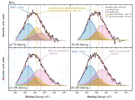
Figure 1.
XPS deconvolution of activated boron and the combination of boron vacancy in the p+ diffused layer by the sheet resistance (Rsheet) variation: (a) 70, (b) 80, (c) 100 and (d) 200 ohm/sq.
Figure 2 shows the results of XPS peak analysis of Si2p and O1s orbitals. The Si0 (Si–Si Bonding) peak with a binding energy of 100 eV [20] does not show a significant difference with respect to the change in the Rsheet, but in the case of boron–oxygen bonding binding energy with 533 eV [21], the peak decreases with an increase in the Rsheet. In the case of boron–oxygen bonding, the Bi–Oi (interstitial boron–interstitial oxygen dimer) or BS–Oi (substitutional boron–interstitial oxygen dimer) complex acts as a defect site. The Bi–Oi defect recombination model can exist only in the stable state. However, in the metastable state, it is difficult to describe the recombination defect center as the Bi–Oi defect mechanism. The model developed to describe the defect model in the metastable state is a recombination defect model by BS–O2i, a substitutional boron (BS) and an oxygen atom dimer (O2i) complex. Substitutional boron is largely immobile in the silicon lattice, and there is a negligibly small amount of interstitial boron. Therefore, substitutional boron and oxygen atoms mainly react. In addition, O2i reacts preferentially to the substitutional boron, which is explained by two reasons. The first reason is that the diffusivity in silicon is several times higher in the case of O2i, which is the agglomerates of two interstitial oxygen atoms, compared to interstitial atomic oxygen, and secondly, the tetrahedral covalent radius of the B atom (0.88 Å) is 25% smaller than the Si host atom (1.17 Å) [22]. As the peak of the boron–oxygen complex changes, the recombination center caused by the B–O complex decreases, resulting in the minority carrier lifetime, iVoc, and the saturation current density of the p+ diffused layer. This leads to the change in the electrical properties and affects the output characteristics of the solar cell.
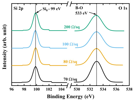
Figure 2.
XPS analysis of silicon (binding energy (BE) ≅ 100 eV) and the boron–oxygen complex (BE = 533 eV) in the p+ diffused layer by Rsheet variation with Si2p and O1s peak intensity.
Figure 3 analyzes the electrical properties of the p+ diffused emitter by the relative ratio of the activated boron (binding energy (BE) = 187.8 eV) and interstitial defect boron (BE = 186.7 eV) peaks, obtained through the previous XPS analysis. The ratio of the activation/interstitial boron peaks shown on the x-axis is 0.58, 1.81, 1.89 and 2.24, and the Rsheet of the p+ diffused layers are 70, 80, 100 and 200 ohm/sq, respectively.
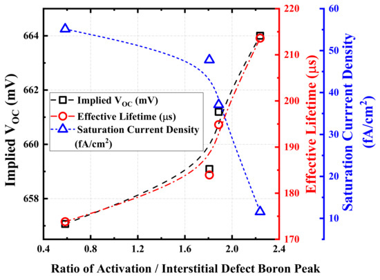
Figure 3.
Open-circuit voltage (iVoc), effective carrier lifetime and saturation current density trend with respect to the activation/interstitial defect boron peak ratio within p+ diffused layer conditions.
The electrical properties of the p+ diffused layer, such as effective lifetime, iVoc and saturation current are obtained by the following formula [23,24].
where k is the Boltzmann constant, T is Kelvin temperature, JSC is current density at 1-sun illumination, τSRH is the bulk Shockley–Read–Hall (SRH) lifetime, τAuger is the bulk Auger lifetime, J0,total is the total saturation current density, q is the elementary charge, ni is the intrinsic carrier density, Δn is the excess carrier concentration and W is the wafer thickness. The open-circuit voltage, in which the final output characteristics of the solar cell are directly proportional to the minority carrier lifetime, saturation current density of the bulk, emitter, back-surface field and total (J0,bulk + J0,emitter + J0,BSF = J0,total), is inversely related, respectively. The decrease in saturation current density in the p+ diffused layer reveals that the activated boron has diffused significantly so that the electrical property degradation caused by the defect site is minimized, leading to an improvement in the minority carrier lifetime and an increase in the open-circuit voltage and, hence, conversion efficiency of the solar cell.
Figure 4 shows the results of the minority carrier lifetime and iVoc obtained by depositing SiNx with a positive charge, an AlOx thin film with a negative charge and a thermally grown SiO2 thin film with a neutral charge as a passivation layer [25] on the p+ diffused layer with variable Rsheet (activation/interstitial boron peak ratio change). For passivation of the p+ diffused layer, it is effective to improve the carrier lifetime and open-circuit voltage using AlOx with a negative charge or an SiO2 layer with a neutral charge. Conversely, the SiNx layer that has a positive charge is not suitable for passivation of the p+ diffused layer due to the deterioration of its properties. In the case of the SiNx single layer, the iVoc is limited to the maximum 655 mV, whereas in the case of the sample applied with AlOx/SiNx, it can be confirmed that when the FGA (forming gas annealing) process [26] is performed after fast-firing, it reaches from a minimum of 661 to a maximum of 670 mV. Based on this result, the passivation of the p+ diffused layer and the difference in iVoc of about 6 to 15 mV remains dependent on the charge polarity, which is the difference between the SiNx and AlOx layers.
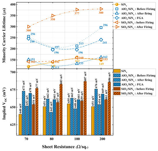
Figure 4.
Variation in minority carrier lifetime and iVoc with respect to the passivation layer (SiNx, AlOx/SiNx and SiO2/SiNx) and the Rsheet.
It can be seen that the passivation quality of the thermally grown SiO2 thin film is superior in terms of lifetime and iVoc to that of AlOx/SiNx, which is due to the difference in interface trap density between the thin film formed in the PECVD and the thermal furnace.
When AlOx is deposited on the surface of the p+ diffused layer, an accumulation layer is formed by a negative charge, and field effect passivation is performed on the p+ diffused layer. As can be seen in Figure 4, the SiNx layer passivation characteristic represented by the yellow line and bar is inferior to the AlOx/SiNx double-stacked layer passivation characteristic represented by the blue line and bar. When the fast-firing process is performed after the deposition of the AlOx/SiNx layer, degradation of the minority carrier lifetime and iVoc characteristics occurs. Additionally, after undergoing the FGA process, the degradation due to firing is recovered. The quality of passivation between the AlOx and p+ diffused layer is lowered by thermal stress when fast-firing, and the lifetime and iVoc are recovered due to the hydrogen covering the dangling bond of the p+ surface through the FGA process.
Figure 5 shows the external quantum efficiency of the solar cells made with different Rsheet. These samples were passivated with the optimized AlOx/SiNx layer. When the ratio of quantum efficiency at 300 nm wavelength was assumed to be 100% with the 200 ohm/sq sample, the blue response also increases with 88%, 92% and 94% as the Rsheet increases, respectively. A higher Rsheet will contribute to increase the short wavelength absorption, and when the emitter is heavily doped (lower Rsheet), the spectral response at short wavelength characteristics is decreased. As can be seen in the analysis of the boron–silicon–oxygen bonding phenomenon through the XPS, minority carrier lifetime and iVoc, the change of the active/interstitial defect boron ratio and B–O bonding complex decreased in boron–silicon bonding coordination. The quantum efficiency of the p+ diffused layer, which acts as an emitter in the n-type-based c-Si solar cell, can also be confirmed by the improvement of properties as the Rsheet increases.
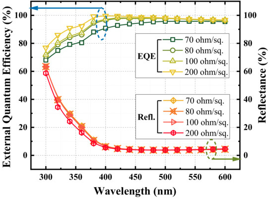
Figure 5.
External quantum efficiency and reflectance analysis with respect to Rsheet variation.
Figure 6 shows the loss analysis carried out for optimization and contributed to the efficiency improvement, such as the loss in emitter, bulk, BSF and contact region. The loss analysis was carried out using the TCAD program. The optimized values obtained from Figure 3 for the 70, 80, 100 and 200 ohm/sq Rsheet were inputted into the TCAD program. The front surface recombination velocity values were varied, and we obtained a conversion efficiency of 20.15%, 20.52%, 20.59% and 20.61%, respectively.
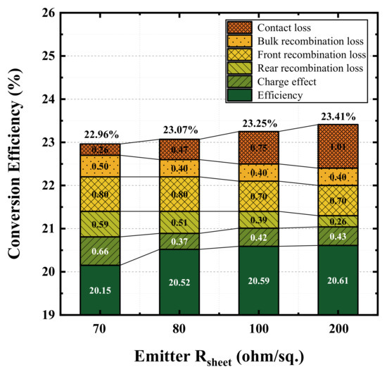
Figure 6.
Loss analysis using TCAD simulation to achieve conversion efficiency over 23% with respect to the optimized Rsheet.
In this TCAD simulation, five key parameters were selected for efficiency improvement and optimization: the “charge effect”, which applies negative charge to improve the characteristics of the front passivation layer; “front and rear recombination loss”, which is based on the quality of the interface trap density of the front and rear passivation layer; wafer quality, to reduce the “bulk recombination loss”; and “contact loss”, indicating the contact characteristics between the p+ diffused layer and front electrode. In the TCAD simulation, the baseline contact resistance was assumed to be 5 mΩ∙cm−2 and varied the contact resistance in steps of 0.5 mΩ∙cm−2 during optimization [27]. The front and rear recombination loss parameters were optimized by varying the front and rear surface recombination velocities from 900 to 600 cm/s in steps of 10 cm/s, respectively [28,29,30].
Though there is potential for improvement of conversion efficiency with the increase in the emitter Rsheet, there are few other key parameters needed to be optimized based on the Rsheet. The major parameter showing the largest change is the loss due to the contact resistivity of the p+ emitter and the front finger. In the case of the 70 ohm/sq, the ratio of contact loss to the overall efficiency improvement range is 9.25%, but in the 200 ohm/sq, it accounts for 36.07%. This is because the surface concentration related to the contact resistance is relatively low as the Rsheet increases. To compensate the contact loss caused by the increase in the Rsheet, optimization of the Ag–Al (Silver–Aluminum) paste [31], selective emitter technology [32] and plating using a seed layer [33] can be considered.
Next is the front recombination loss and charge effect. On average, the conversion efficiency of both parameters increased by 0.75% and 0.47%. In order to achieve high efficiency, the passivation layer, either the AlOx layer deposited by ALD (atomic layer deposition) or the thermally grown SiO2 thin films containing a negative or neutral charge are suitable to reduce the recombination compared to the PECVD process. The rear-side recombination loss and bulk properties were 0.44% and 0.425%, respectively, which contributed to the improvement of conversion efficiency.
4. Conclusions
For the high efficiency of crystalline silicon solar cells using n-type substrates, the optimization of electrical properties of boron diffusion and the emitter, which are the most basic properties, was examined in terms of boron–silicon coordination bonding and oxygen complexes. The change in the electrical properties depends on the ratio of activation/interstitial boron peaks in the boron-diffused layer, the charge polarity and the passivation layer of the p+ diffused surface. The experimental values were incorporated into the TCAD simulation, and loss analysis was carried out. The recombination losses at the front and rear and the contact loss must be minimized to achieve high-efficiency silicon solar cells.
Author Contributions
Conceptualization and writing—original draft preparation, C.P.; data curation, G.S.; writing—review and editing, N.B. and J.P.; supervision, J.Y. All authors have read and agreed to the published version of the manuscript.
Funding
This research received no external funding.
Acknowledgments
This work was supported by the Korea Institute of Energy Technology Evaluation and Planning (KETEP) grant funded by the Korea government (MOTIE) (20203030010310) and This work was supported by the National Research Foundation of Korea (NRF) grant funded by the Korea government (MSIT) (No. NRF-2019R1A2C1009126).
Conflicts of Interest
The authors declare no conflicts of interest.
References
- Glunz, S.W.; Rein, S.; Lee, J.Y.; Warta, W. Minority carrier lifetime degradation in boron-doped Czochralski silicon. J. Appl. Phys. 2001, 90, 2397–2404. [Google Scholar] [CrossRef]
- Lv, Y.; Zhuang, Y.F.; Wang, W.J.; Wei, W.W.; Sheng, J.; Zhang, S.; Shen, W.Z. Towards high-efficiency industrial p-type mono-like Si PERC solar cells. Sol. Energy Mater. Sol. Cells 2020, 204, 110202. [Google Scholar] [CrossRef]
- International Technology Roadmap for Photovoltaic (ITRPV); VDMA: Penang, Malaysia, 2019.
- Nandakumar, N.; Rodriguez, J.; Kluge, T.; Groβe, T.; Fondop, L.; Padhamnath, P.; Balaji, N.; König, M.; Duttagupta, S. Approaching 23% with large-area monoPoly cells using screen-printed and fired rear passivating contacts fabricated by inline PECVD. Prog. Photovolt. Res. Appl. 2018. [Google Scholar] [CrossRef]
- Feldmann, F.; Bivour, M.; Reichel, C.; Steinkemper, H.; Hermle, M.; Glunz, S.W. Tunnel oxide passivated contacts as an alternative to partial rear contacts. Solar Energy Mater. Solar Cells 2014, 131, 46–50. [Google Scholar] [CrossRef]
- Stodolny, M.K.; Lenes, M.; Wu, Y.; Janssen, G.J.M.; Romijn, I.G.; Luchies, J.R.M.; Geerligs, L.J. n-Type polysilicon passivating contact for industrial bifacial n-type solar cells. Solar Energy Mater. Solar Cells 2016, 158, 24–28. [Google Scholar] [CrossRef]
- Richter, A.; Benick, J.; Feldmann, F.; Fell, A.; Hermle, M.; Glunz, S.W. n-Type Si solar cells with passivating electron contact: Identifying sources for efficiency limitations by wafer thickness and resistivity variation. Solar Energy Mater. Solar Cells 2017, 173, 96–105. [Google Scholar] [CrossRef]
- Chen, Y.; Chen, D.; Liu, C.; Wang, Z.; Zou, Y.; He, Y.; Wang, Y.; Yuan, L.; Gong, J.; Lin, W.; et al. Verlinden. Prog. Photovolt. Res. Appl. 2019, 27, 827–834. [Google Scholar] [CrossRef]
- Schiele, Y.; Joos, S.; Hahn, G.; Terheiden, B. Etch-back of p+ Structures for Selective Boron Emitters in n-type c-Si Solar Cells. Energy Procedia 2014, 55, 295–301. [Google Scholar] [CrossRef][Green Version]
- Basu, P.K.; Khanna, A. A new single-component low-cost emitter etch-back process for silicon wafer solar cells. Clean Technol. Environ. Policy 2017, 19, 1655–1665. [Google Scholar] [CrossRef]
- Tao, Y.; Madani, K.; Cho, E.; Rounsaville, B.; Upadhyaya, V.; Rohatgi, A. High-efficiency selective boron emitter formed by wet chemical etch-back for n-type screen-printed Si solar cells. Appl. Phys. Lett. 2017, 110. [Google Scholar] [CrossRef]
- Clugston, D.A.; Basore, P.A. PC1D version 5: 32-bit solar cell modeling on personal computers. In Proceedings of the Conference Record of the Twenty Sixth IEEE Photovoltaic Specialists Conference, Anaheim, CA, USA, 29 September–3 October 1997; pp. 207–210. [Google Scholar]
- Fell, A.; McIntosh, K.R.; Altermatt, P.P.; Janssen, G.J.M.; Stangl, R.; Ho-Baillie, A.; Steinkemper, H.; Greulich, J.; Muller, M.; Min, B.; et al. Input Parameters for the Simulation of Silicon Solar Cells in 2014. IEEE J. Photovolt. 2015, 5, 1250–1263. [Google Scholar] [CrossRef]
- Kramer, N.J.; Schramke, K.S.; Kortshagen, U.R. Plasmonic Properties of Silicon Nanocrystals Doped with Boron and Phosphorus. Nano Lett. 2015, 15, 5597–5603. [Google Scholar] [CrossRef] [PubMed]
- Yamauchi, J.; Yoshimoto, Y.; Suwa, Y. Identification of boron clusters in silicon crystal by B1s core-level X-ray photoelectron spectroscopy: A first-principles study. Appl. Phys. Lett. 2011, 99, 191901. [Google Scholar] [CrossRef]
- Yamauchi, J.; Yoshimoto, Y.; Suwa, Y. X-ray photoelectron spectroscopy analysis of boron defects in silicon crystal: A first-principles study. J. Appl. Phys. 2016, 119, 175704. [Google Scholar] [CrossRef]
- Tsutsui, K.; Matsuda, T.; Watanabe, M.; Jin, C.-G.; Sasaki, Y.; Mizuno, B.; Ikenaga, E.; Kakushima, K.; Ahmet, P.; Maruizumi, T.; et al. Activated boron and its concentration profiles in heavily doped Si studied by soft x-ray photoelectron spectroscopy and Hall measurements. J. Appl. Phys. 2008, 104. [Google Scholar] [CrossRef]
- Solmi, S.; Landi, E.; Baruffaldi, F. High-concentration boron diffusion in silicon: Simulation of the precipitation phenomena. J. Appl. Phys. 1990, 68, 3250–3258. [Google Scholar] [CrossRef]
- Park, C.; Kim, B.; Balaji, N.; Lee, Y.J.; Ju, M.; Lee, H.; Yi, J. Boron Oxygen Pair Effect in p+ Emitter and Nanosized Boron Rich Layer by Fold Coordination Analysis for Crystalline Silicon Solar Cell Applications. J. Nanosci. Nanotechnol. 2016, 16, 4846–4850. [Google Scholar] [CrossRef]
- Kolel-Veetil, M.K.; Gamache, R.M.; Bernstein, N.; Goswami, R.; Qadri, S.B.; Fears, K.P.; Miller, J.B.; Glaser, E.R.; Keller, T.M. Substitution of silicon within the rhombohedral boron carbide (B4C) crystal lattice through high-energy ball-milling. J. Mater. Chem. C 2015, 3, 11705–11716. [Google Scholar] [CrossRef]
- Soto, G. Hot Filament Chemical Vapor Deposition of Crystalline Boron Films. J. Korean Ceram. Soc. 2019, 56, 269–276. [Google Scholar] [CrossRef]
- Schmidt, J.; Bothe, K. Structure and transformation of the metastable boron- and oxygen-related defect center in crystalline silicon. Phys. Rev. B 2004, 69, 024107. [Google Scholar] [CrossRef]
- Benick, J.; Hoex, B.; van de Sanden, M.C.M.; Kessels, W.M.M.; Schultz, O.; Glunz, S.W. High efficiency n-type Si solar cells on Al2O3-passivated boron emitters. Appl. Phys. Lett. 2008, 92, 253504. [Google Scholar] [CrossRef]
- Wei, Y.; Jiang, X.; Lin, Y.; Yang, X.; Li, G.; Liu, X.; Li, P.; Liu, A. Analysis and optimization of alloyed Al-p+ region and rear contacts for highly efficient industrial n-type silicon solar cells. RSC Adv. 2019, 9, 6681–6688. [Google Scholar] [CrossRef]
- Dingemans, G.; Kessels, W.M.M. Status and prospects of Al2O3-based surface passivation schemes for silicon solar cells. J. Vac. Sci. Technol. A Vac. Surf. Film. 2012, 30, 040802. [Google Scholar] [CrossRef]
- Dhungel, S.K.; Yoo, J.; Kim, K.; Karunagaran, B.; Sunwoo, H.; Mangalaraj, D.; Yi, J. Effect of pressure on surface passivation of silicon solar cell by forming gas annealing. Mater. Sci. Semicond. Process. 2004, 7, 427–431. [Google Scholar] [CrossRef]
- Schroder, D.K.; Meier, D.L. Solar cell contact resistance—A review. IEEE Trans. Electron Devices 1984, 31, 637–647. [Google Scholar] [CrossRef]
- Hoex, B.; Heil, S.B.S.; Langereis, E.; van de Sanden, M.C.M.; Kessels, W.M.M. Ultralow surface recombination of c-Si substrates passivated by plasma-assisted atomic layer deposited Al2O3. Appl. Phys. Lett. 2006, 89, 042112-1–042112-3. [Google Scholar] [CrossRef]
- Hoex, B.; Schmidt, J.; Bock, R.; Altermatt, P.P.; van de Sanden, M.C.M.; Kessels, W.M.M. Excellent passivation of highly doped p-type Si surfaces by the negative-charge-dielectric Al2O3. Appl. Phys. Lett. 2007, 91, 112107-1–112107-3. [Google Scholar] [CrossRef]
- Hoex, B.; Gielis, J.J.H.; van de Sanden, M.C.M.; Kessels, W.M.M. On the c-Si surface passivation mechanism by the negative-charge-dielectric Al2O3. J. Appl. Phys. 2008, 104, 113703. [Google Scholar] [CrossRef]
- Wöhrle, N.; Lohmüller, E.; Greulich, J.; Werner, S.; Mack, S. Towards understanding the characteristics of Ag–Al spiking on boron-doped silicon for solar cells. Sol. Energy Mater. Sol. Cells 2016, 146, 72–79. [Google Scholar] [CrossRef]
- Ding, D.; Lu, G.; Li, Z.; Zhang, Y.; Shen, W. High-efficiency n-type silicon PERT bifacial solar cells with selective emitters and poly-Si based passivating contacts. Sol. Energy 2019, 193, 494–501. [Google Scholar] [CrossRef]
- Recamán Payo, M.; Li, Y.; Russell, R.; Singh, S.; Kuzma Filipek, I.; Duerinckx, F.; Szlufcik, J.; Poortmans, J. Efficiency gain in plated bifacial n-type PERT cells by means of a selective emitter approach using selective epitaxy. Sol. Energy Mater. Sol. Cells 2020, 204, 110173. [Google Scholar] [CrossRef]


© 2020 by the authors. Licensee MDPI, Basel, Switzerland. This article is an open access article distributed under the terms and conditions of the Creative Commons Attribution (CC BY) license (http://creativecommons.org/licenses/by/4.0/).