Abstract
The paper briefly discusses the most important standards and regulations established for high-power wireless power transfer systems and introduces the main issues concerned with the conceptual design process. It analyses the electromagnetic design of the inductive magnetic coupler and proposes key formulas to optimize its electrical parameters for a particular load. The method applies to both the resistive load and the battery charging. It also suggests basic topologies for conceptual design of power electronics and discusses its proper connection to the grid. The proposed design strategy is verified by experimental laboratory measurement including analyses of the leakage magnetic field.
1. Introduction
In addition to regulations on wireless charging and its commercialization, it is necessary to consider a number of other important technical issues in the design of the system. Energy efficiency and power density are the most important qualitative indicators [1,2] of any power electronic system and key factors leading to their continual increase have an environmental as well as an economic character. Nowadays, in the industrial and consumer electronics market, the international standards and regulations are determined by international organizations like, U.S Energy Star, 80 Plus, Climate Savers, German Blue Angel, etc. Therefore, wireless power transfer (WPT) systems will face contradictory requirements imposed on their individual construction components (power converter, coupling coils, compensation capacitors etc.…). The regulations concerning qualitative indicators of semiconductor power systems are completely different from the regulations defined for WPT operation; hence, it is a complex task to design a high-performance WPT system that will comply with all technical and safety regulations at once.
Another important issue is WPT system lifetime. It is known that several configurations [3,4,5,6] of the resonant tank can be used according to the target application. When talking about battery charging in the automotive industry, the series–series compensation topology is the best choice [7,8,9]. In that case, the compensation capacitors are stressed [10] with a relatively high voltage (usually several kilovolts) and, therefore, either a series–parallel connection of individual capacitors or bulky high-end capacitors need to be used. However, both options have their pros and cons and are closely related to the thermal stability and consequently to the relative tolerance of component values. This has a direct impact on the lifetime performance and, therefore, the most suitable solution for targeted applications must be found. The commercial uses of WPT systems have also been widely discussed due to biocompatibility issues [11,12,13,14]. Several standards are now available [15,16] as guidelines for safety when the interaction between the EM field and living organisms is considered. Therefore, EM field shielding [17,18,19,20] is also a very important component that must be included in the system design. The literature proposes several analyses focused on this topic, but only a few of them are supported by leakage field measurements.
This paper gives an outline of design process for high-power wireless chargers suitable for e-mobility and points out some technical issues and possible solutions. It recapitulates basic standards and regulations and discusses issues concerned with EM field shielding. It further proposes key formulas to optimize the electrical parameters of inductive couplers and suggests basic topologies for conceptual design of power electronics, including proper connection to the power grid.
2. Wireless Power Transfer Standards and Regulation
As wireless charging becomes an increasingly discussed issue, addressed not only by academic researchers but also by industrial subjects, standardization is required for smooth and reliable commercialization.
This should allow interoperability between different chargers and increase safety. Therefore, the standards must include safety and efficiency criteria, EM field limits, and interoperability targets along with wireless charging testing. Among the most important standards for WPT is SAE TIR J2954/2 [21], which is concerned with alignment methods, interoperability, and frequency band and power levels. It establishes an efficiency greater than 90% when using matched coils and higher than 85% when using interoperable systems.
Since wireless charging is accompanied by a high-frequency electromagnetic field, it is also necessary to control the EM field levels. ICNIRP 2010 [15] specifies guidelines for the protection of humans exposed to electric and magnetic fields in the specific frequency range of the electromagnetic spectrum. Another guideline is established in the IEEE standard for safety levels with respect to human exposure to radio frequency electromagnetic fields of 3 kHz to 300 GHz (IEEE Std C95.1a™ 2010) [16]. The reference level for exposure to time-varying EM fields (RMS values) is shown in Figure 1.
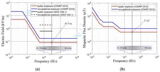
Figure 1.
Reference level for exposure to time-varying electric (a) and magnetic (b) fields [15,16].
To meet these standards, it is necessary to keep levels of the EM field below 27 µT and 83 V/m at a resonant frequency of 85 kHz (81.39 ÷ 90 kHz).
3. Magnetic Coupler Design
In the case of inductive coupling wireless power transmission, the system acts as an air-cored transformer achieving very low mutual inductance. To achieve high voltage-gain and high efficiency, it is desirable to operate the system at resonance. Therefore, the external capacitor is connected to the coupling coil on the primary and the secondary to compensate the inductive reactance.
The literature [3,4,5] involves four typical compensation topologies. These could be classified as series–series, parallel–parallel, series–parallel and parallel–series compensation. As many authors have already presented [7,8,9], the series–series topology (see Figure 2) provides us with numerous important benefits, particularly for battery charging, so it is usually used for this purpose.
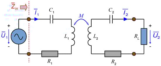
Figure 2.
Series-series compensation topology.
Here, the parameters R1 and R2 represent the equivalent series resistances; L1 and L2 introduce self-inductances; M forms the mutual inductance measured between both coils; and ω is the angular frequency of the supply voltage.
The secondary-side capacitor is usually selected according to the required operational resonant frequency f0 = ω0/2π, so it completely compensates self-inductance of the secondary coil. Its value is given by (1).
Then, the primary-side capacitor is calculated based on (2), using a cancellation of the imaginary part of total reflected impedance.
With the application of (1) to (2), we get (3).
Hence, both capacitors are independent of mutual inductance, which prevents the system from tuning the capacitors when changing the position between magnetic couplers. Moreover, they are of exactly the same values when the coupling coils are identical. Based on this, we may assume (4).
In that case, the secondary current is calculated as (5).
Additionally, as we want to minimize I2R losses, we need to design the coupling coils so that they have the least series resistance. In the first approximation, we can consider the resistance to be zero. This assumption simplifies (5) into (6).
From (6), we may conclude that the secondary current is proportional to the input voltage and inversely proportional to the product of . In other words, the secondary current is independent of the load, which is particularly beneficial to high-power battery charging.
The highest theoretically achievable efficiency is defined as (7).
Here, k represents the magnetic coupling coefficient measured between coils, and Q1 and Q2 represent their quality factors.
Equation (7) means that the larger the product, (8), the higher the achievable efficiency is. Therefore, the product, (8), represents the figure-of-merit (FOM) of the system.
Considering (7), we know there is an existing maximum of efficiency that could be reached, but, in general, only the value of the load determines the efficiency. Therefore, it is necessary to find the optimal value of the load which will lead to efficiency maximization.
The searched value is defined by (9).
Assuming zero I2R losses, we get the simplest equation, Equation (10).
In previous work [21], the authors demonstrate that a load (ohmic value) lower than the optimal load causes a significant decrease in efficiency and transmitted power. This might be partially compensated by frequency tuning, but still we are limited by the frequency band recommended by the SAE TIR specification [22].
On the other hand, the higher loads work well with the system and cause no additional problem. Therefore, it is reasonable to design the system such that it operates with load defined by (9) or higher. As an example, we can consider a typical battery charging cycle (see Figure 3) of the EV Nissan Leaf [23].
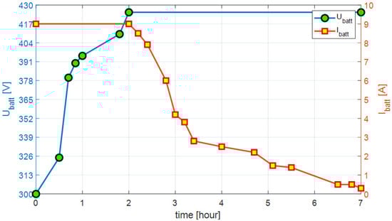
Figure 3.
Battery charging cycle of Nissan Leaf [24].
Another possibility is to use a dc/dc converter on the secondary side for direct active regulation of the equivalent load (see Figure 5).
As seen in Figure 3, during the first two hours, the charger supplies the battery with a constant current (full power) to reach the nominal voltage, and then the current falls down slightly while the voltage is kept constant. This charging diagram might be recalculated in equivalent load, which is continuously rising. Thus, it is possible to design the couplers for the load being observed by the system during the constant-current interval (the first two hours). This will lead to a high operational efficiency during the whole charging cycle.
According to situation seen in Figure 4, the equivalent operational load is also determined from the battery voltage Ubatt and the charging power P2.
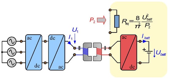
Figure 4.
Typical WPT system configuration.
Moreover, the secondary-side rectifier reflects the resulting load impedance from the dc side to its ac value and must be therefore recalculated according to (11).
Comparing (10) to (11), it is easy to find the value of mutual inductance (12) necessary to reach the required charging power for a given battery pack.
As we come out of the optimal load, it also gives us high efficiency for transferring power. Formula (12) could also be derived from the input current I1, so we have relation (13).
As stated by (8), mutual inductance together with frequency both predefine the maximum system efficiency. Sometimes, the input voltage U1 is limited and, consequently, the resulting FOM may be too small for power applications. In that case, it is possible to increase the voltage on the primary and decrease it on the secondary by using two additional dc/dc converters connected according to Figure 5.
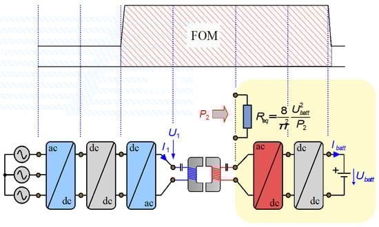
Figure 5.
Typical WPT system configuration including dc/dc converters.
Either way, the voltage measured across the coupling coil must be considered carefully with respect to the EM field limits referred to in INCNIRP 2010 [15]. The same holds also for the magnetic field. Hence, it is about balancing the electric and the magnetic field levels. With a higher voltage, we reduce the flux density, and vice versa.
The method described above gives us all the necessary electrical parameters needed for the magnetic design (real geometry of the coils). The goal is therefore to design the geometry of the couplers so they will form the mutual inductance according to (12) or (13) and have the series resistance as low as possible.
The mounting dimensions are usually restricted by assembly space available on the vehicle. Together with presumed working distance, we can estimate the coupling coefficient k and consequently the self-inductance L.
Based on the chosen coupler design (coil structure, shielding, materials …), it is possible to calculate a proper number of turns. An interesting analytical approach is shown in [22].
The coils should be wound with a gap between each turn to prevent high parasitic capacitance, which would significantly decrease the quality factor. The spatial distribution of current (i.e., proximity effect) within neighboring wires must also be considered since it strongly affects the series resistance of the coils. Hence, the insulated high-frequency cables with strands whose diameter is smaller than the skin depth are usually used for windings.
Several coupler designs are very popular and most commonly used for power EV charging, e.g., single-coil structure or multi-coil structures [25,26,27,28,29,30]. They are usually organized as follows: the windings sit above the ferrite shielding which guides most of the flux under the coil. Then, the aluminum shield is added to the back of the ferrites to protect surrounding objects from any effects of leaked EM field. This is particularly important for EV charging because the vehicle floor is typically made out of steel.
Without the shielding, the leakage flux would induce eddy currents into the vehicle and consequently would increase the losses as well as influence the coil quality factor.
A single-coil structure, as seen in Figure 6a, can be designed as a circular or rectangular shape, and is most often discussed and reported in literature [28,29,30] because it is simple and cheap. Its main disadvantage lies in the shape of the fundamental flux path. The flux goes from the transmitter to the receiver through their geometrical center and then it returns back through the leakage path (outside the couplers). As a consequence, the configuration introduces a lower coupling coefficient then other types of similarly sized coils and puts higher demands on shielding against EM fields.
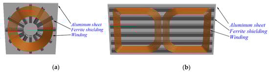
Figure 6.
Flat circular coil coupler (a); Double D coupler configuration (b).
An improved topology is shown in Figure 6b. It is known as the Double D (DD) configuration [28,29,30] because of the ideal D shape of the coils sitting back to one another. The two coils are connected in series magnetically and, therefore, they guide the flux into a closed path. This single-sided flux pattern significantly reduces the leakage flux and simultaneously increases the coupling coefficient.
The next evolutionary step (Figure 7) is a polarized coupler labeled as DDQ [28,29,30], which is derived from the DD configuration by adding the quadrature Q-coil. Both coils are magnetically decoupled and, therefore, they could be used independently. The strong advantage is that the DDQ can capture both the direct component and the quadrature component of the flux, so it features higher tolerance to misalignment and is fully interoperable with a circular coil or DD coil. However, the size of DDQ coils is increased approximately three times relative to the circular or the square coils.
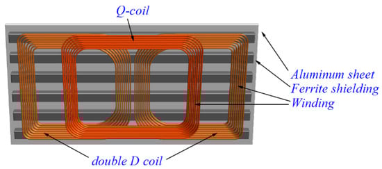
Figure 7.
Double D&Q (DDQ) coupler configuration.
The literature involves several other derived topologies, but they are not so often discussed or actually used as those we have mentioned here.
4. Power Electronics Configuration
Most designers assume a standard network connection and, therefore, the goal is to achieve the power consumption with highest possible power factor. This, in addition, requires a fully symmetrical three-phase current having as low a total harmonic distortion THDi as possible.
In (14), iac (μ) represents the μ-th harmonic component of the power grid current. Thus, the active input rectifier or the combination of passive rectifier with the power factor correction (PFC) must be used on the system primary side.
The second proposed configuration has a complex structure, consisting of input active or passive PFC, active or passive total harmonic distortion correction (THDC), a diode rectifier, a dc/dc converter (step-up or step-down) and a voltage source inverter. Such configuration is robust and verified by many similar applications, while the only drawback lies in its higher price and build-in dimensions along with an increase in power rating. This topology should therefore be recommended for low- or medium-power WPT systems.
For medium- or high-power WPT systems, it is recommended to use the configuration consisting of input inductance (formed by distribution transformer or by external one), the active rectifier and the voltage source inverter. This topology can provide a smooth input current, having almost sinusoidal shape, quite low THDi, an excellent power factor and a controllable output voltage. Thus, no additional dc/dc converters are needed.
Besides the fact that these circuits affect the quality of the power drawn from the grid, their next task is to prepare the voltage for the input inverter according to FOM (see Figure 5). This is the most critical component of the power electronic system for wireless charging and can be constructed in two different topologies: the half-bridge inverter and the full-bridge inverter. The full-bridge inverter requires a more complex structure and more complicated control algorithms than the half-bridge inverter, but it provides better performance, especially for high-power WPT systems.
The recommended topologies are summarized in Figure 8 according to system dedicated power level. The secondary side is usually designed according to the type of load and includes either the passive or the active rectifier. Finally, the system connection to the grid considering all the power levels established as WPT categories by SAE TIR J2954 is seen in the conceptual layout shown in Figure 9, valid especially for central Europe.
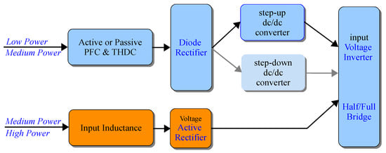
Figure 8.
Power electronics configurations on the primary.
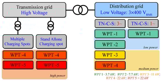
Figure 9.
WPT system categories—connection to the grid.
A practical example of a solution that could meet all necessary technical requirements for high-power applications while having excellent operational properties is seen in Figure 10.
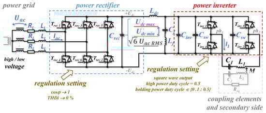
Figure 10.
Recommended system configuration for high-power applications.
In Figure 10, the input dc filter Crec is added to improve any voltage fluctuation ΔUdc caused by principle of rectifier operation and its actual regulation settings. The optimal value of Crec depends on the power consumption conditions. Regarding power grid frequency f1, expected voltage ripple ΔUdc (maximum 10% of UDC max) and maximum value of dc bus voltage Udc max (continues regulation of UDC considered), we may write (15).
The input inverter capacitor (Csw & Cinv) is composed of two types of capacitors connected in parallel; first, the switching capacitor Csw (low capacitance, fast in operation) and, second, the filtering capacitor Cinv (high capacitance, not slow in operation). The resulting capacitance should be designed as (16).
If the active rectifier (having m input phases) operates at the switching frequency facdc, we can write (17) with respect to the specific voltage ripple ΔUCinv (at maximum 10% of UDC max) measured on the input of the inverter.
The value of inductance Ldc is then given by (18).
Since the inverter draws impulse power due to the second harmonic component of the current flowing through the coupling coil, a resonant filter (Lf and Cf) tuned to the frequency 2f0 must be installed in the DC bus. Thus, the filter capacitance Cf equals and the inductance Lf must fulfill (19).
Finally, the input inductance LL, which must cover requirements on any increase of dc bus voltage, is determined from modulation index mi and demanded current ripple ΔIac as (20).
The inverter supplies the resonant circuit at the resonant frequency, which means that it is operated in the current soft switching mode. This fact also has a direct impact on the selection of used semiconductor devices (usually fast SiC or GaN).
The secondary side of the system, shown in Figure 10, is drawn in more detail in Figure 11. Looking at the circuit from the left to the right, it comprises a magnetic coupler, diode rectifier including filter CS, dc/dc step-down converter (SD) and on-board battery pack.
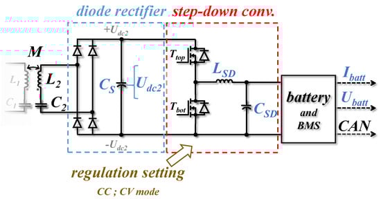
Figure 11.
Recommended system configuration for high-power applications.
To maintain a defined voltage ripple ΔUCs measured on the diode rectifier output, the filter Cs has to be designed according to Equation (21).
The smoothing inductance LSD can significantly improve the charging process, and, for any setting of the step-down converter, duty cycle s and the battery current ripple ΔIbatt can be determined from (22). Here, fSD represents the switching frequency of SD.
Finally, the capacitance CSD must be added to prevent any unwanted parasitic resonance with the battery capacitance. Its approximate value is given in (23).
According to the required high system efficiency (required more than 90%) and high switching frequency (especially for inverter and rectifier—85 kHz band) a new generation of semiconductors were taken into account. In our calculations, we consider SiC semiconductors (full SiC MOSFETs and SiC diodes). The GaN semiconductors are also usable; however, there is a problem with high blocking voltage according to the FOM design. SiC semiconductors have very a small turn-off and very small losses (hundreds of micro-joules), with a very low switching time (less than ten nano-seconds). This rapidly decreases switching loses and rapidly increases possible switching frequency. The on-state power loses are also small (ones of mwcm-2), which reduces conduction loses and contributes to great efficiency as well.
5. Control and Drive Methods
The proposed system configuration makes it possible to safely operate the traction battery within a wide range of CCCV (constant current–constant voltage) charging cycles. However, the charging itself is just one of the three main tasks of a wireless charger. The second important task is to reach very high efficiency, even under different operating conditions. Finally, the third is to maintain a high-quality connection to the power grid. Therefore, the control system usually includes algorithms designed to meet all these requirements simultaneously.
The charging station is usually connected to the power grid through an active voltage pulse rectifier (ideally, three-phase VPR). It controls the power consumption quality in terms of zero phase shift angle measured between leg-voltage and current to keep the THD very low while keeping stable voltage of DC link. The voltage is driven by a higher control level or by a combination of FOM and coupling element design.
Another very important device is the inverter. The output frequency and the voltage must be controlled independently. As the frequency may change a little with changing load, the key part of inverter control is the current–voltage phase lock loop (PLL).
The last controllable part is DC–DC converter (based on FOM), designed as the voltage step down topology. This holds the output voltage in the battery voltage operating area. Of course, based on the higher control level, this should secure battery charging in CCCV mode.
The mentioned low-level controls are covered by an upper level control which respects the transfer efficiency control and CCCV requirements of the battery. The communication between transmitter and receiver (and battery) wireless battery charging station is also important because of the mutual interconnection of low-level controls under the high-level control. The separate receiver and transceiver parts of the wireless charging station lead to the two microcontroller and blocks interfaces (the measure and semiconductor drive). Problems related to proper control have already been discussed in detail in [31], while the described techniques are relevant for the proposed design of the WPT system.
6. Experimental Prototype and Validation Measurements
To demonstrate the validity of the proposed conceptual design strategy, an experimental prototype of wireless charging system utilizing circular shaped coupling coils was designed (Figure 12). The couplers are wound of litz wire (38 AWG) containing 330 insulated strands of diameter 0.1 mm. In order to reduce the parasitic capacitance as much as possible, both coils are wound with a constant turn-to-turn air gap (5 mm long). The inner/outer coil radius is 20/200 mm. The winding has 36 turns, which have a series resistance R1 = R2 = 0.3 Ω, and, together, with the EM field shielding (Figure 12) form the self-inductance L1 = L2 = 218 µH.
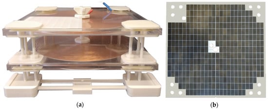
Figure 12.
Coupling coils with positioning mechanism (a) and EM field shielding (b).
Figure 13 shows a block diagram of experimental WPT charger configuration, which reflects the generalized proposal given in previous discussions. Due to initial laboratory performance investigations, a low/medium-power alternative (WPT 1) is considered (Figure 8). The main aim of experimenting is to show that the generalized proposal makes it possible to design WPT systems, which achieve the required qualitative parameters relevant for power density, efficiency and EM compatibility levels.
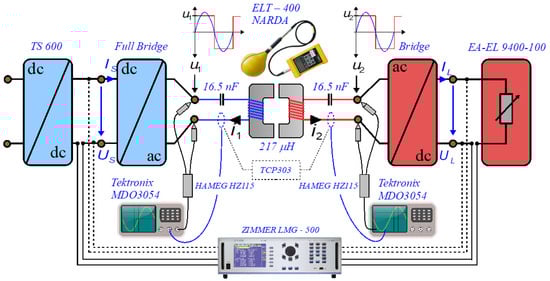
Figure 13.
Schematic diagram of laboratory wiring.
The supply grid is replaced by a configurable DC input source (Magna-Power TS 600), which is connected directly to the primary side inverter, which is designed as a full-bridge converter with SiC switching devices. In order to obtain good operational properties and to reduce the complexity of control, the output rectifier is based on SiC bridge technology supplying a programable electronic load (EA-EL 9400-100). If a practical target application is considered, then it is possible to utilize a secondary side DC/DC converter connected to a bridge SiC rectifier in order to control output voltage/current based on the parameters that are required by the load. The laboratory test stand is shown in Figure 14.
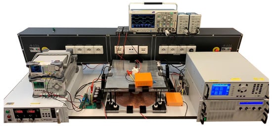
Figure 14.
Experimental laboratory setup of the tested WPT system.
Experimental measurements were focused on precise determination of the efficiency of the coupling coils as well as the efficiency of whole system concept (input-to-output).
The system configuration (Figure 14) enables us easily to evaluate either the overall system efficiency (25), including the power electronics, or the partial efficiency, corresponding to the power transmitted through the magnetic couplers. The input and the output power were measured with a power analyzer ZIMMER LMG 500, having a declared precision of 0.018% of the scale used for currents and 0.034% of the scale used for voltages.
At resonance, the system operates with unity power factor, and then (26) can be used to derive the ac-to-ac efficiency. Here, voltages u1 and u2 represent the amplitudes of the square wave signal. Consequently, they must be recalculated into the RMS values of their fundamental harmonics to obtain the correct powers.
The system was tested with a 20-cm distance arranged between the coupling coils. The resulting mutual inductance M = 24 μH corresponds to the inductive coupling coefficient k = 0.11 [-]. Thus, by using resonant capacitors C = 15.6 nF, we obtain the resonance at frequency f0 = 86.5 kHz. The experimental data are given in Table 1. For better understanding, the ac and the dc values are listed and compared to each other.

Table 1.
Measured experimental data.
The efficiency dependent on the power transmitted to the load is shown in graphical form in Figure 15.
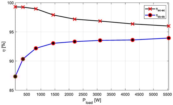
Figure 15.
System efficiency dependent on power delivered to load.
As is obvious, low transmitted power requires a weaker EM field, resulting in very low EM field shielding losses. Consequently, the efficiency of the magnetic coupler is very high. At the same time, the power electronics losses are significant compared to the transmitted power, which results in low overall efficiency. Further, the increasing power makes the EM field stronger and the losses produced by the shielding are higher. Thus, the efficiency of the magnetic coupler decreases continuously. On the other hand, the transmitted power becomes larger compared to the power electronics losses and, therefore, the overall system efficiency is slightly increased (Figure 15).
To evaluate the EM compatibility levels, we analyzed the leakage magnetic field (see in Figure 16) around the coupling coils in the cutting plane with a defined array 180 cm × 180 cm, as defined by ICNIRP 2010 (Figure 1). The leakage field was measured with an exposure level tester ELT 400 Narda when delivering 4.5 kW to the load.
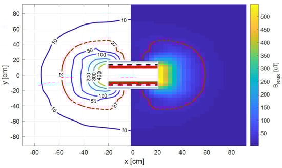
Figure 16.
Leakage magnetic field (RMS values) at 20 cm and 4.5 kW.
The limiting field level (27 μT) defined by ICNIRP 2010 for public exposure is outlined with the dashed red line. As is obvious, the proposed EM field shielding efficiently suppresses the magnetic field component that could affect the cabin of the vehicle. Its shielding capability will further be improved by assembling it on a vehicle, having a floor fabricated from the metal sheets. Optimization is also possible, either by using thicker ferrites or aluminum plates.
The previous experimental testing has confirmed the proposal of a generalized design of WPT chargers in order to meet efficiency and EM compatibility standards required by international norms. It was found that, for the low-power-level WPT concept, the system efficiency was above the required 90% from 5% of nominal power up to the full load. EM compatibility performance was reached above 40 cm of axial and 60 cm of radial distance from the coupling coils center. These results can be further optimized and are valuable for practical design of WPT chargers for automotive or industrial applications.
7. Conclusions
The paper has given a brief recapitulation of most important standards and regulations related to high-power wireless charging systems. It has proposed the magnetic couplers to be designed exactly according to optimal operation to the specific load given by the battery voltage and the charging power. Additionally, it has discussed a solution to improve the FOM of the system with dc/dc converters used on the primary and the secondary sides, relevant especially to low- or medium-power wireless chargers.
For medium- or high-power wireless chargers, we recommend the system composed of input inductance, an active rectifier and a voltage source inverter, which can provide low THDi, excellent power factor and controllable output voltage. Thus, no additional dc/dc converters are needed.
The experimental prototype has proven the validity of the presented physical principles and confirmed the proposed conceptual design strategies. It has also compared ac/ac and dc/dc system efficiency related to loss-to-power-transfer ratio.
Additionally, measurement of the leakage magnetic field has shown the real flux density distribution observed around the circular coupling coils. This could be used for further optimization.
Author Contributions
Conceptualization, M.F., methodology, M.Z., experimental analysis and set-ups, M.P.; writing—original draft preparation, V.K. All authors have read and agreed to the published version of the manuscript.
Funding
This research was funded by the Ministry of Education, Youth and Sports of the Czech Republic under the project OP VVV Electrical Engineering Technologies with High-Level of Embedded Intelligence CZ.02.1.01/0.0/0.0/18_069/0009855 and by funding program of the University of West Bohemia number SGS-2018-009. This research was also funded by national grant agency APVV under project number APVV-0396-15 and APVV-0345-17.
Conflicts of Interest
The authors declare no conflict of interest.
References
- Vasilios, Z.; Papanikolaou, N. Advanced and Intelligent Control in Power Electronics and Drives; Springer International Publishing: Heidelberg, Germany, 2018. [Google Scholar]
- Robert, B.; Francis, L.; Guy, S. Power Electronic Converters DC-DC Conversion; Springer: Berlin, Germany, 2013. [Google Scholar]
- Zhang, W.; Mi, C.C. Compensation topologies of high-power wireless power transfer systems. IEEE Trans. Veh. Technol. 2016, 65, 4768–4778. [Google Scholar] [CrossRef]
- Lu, F.; Zhang, H.; Hofmann, H.; Mi, C.C. An inductive and capacitive combined wireless power transfer system with LC-compensated topology. IEEE Trans. Power Electron. 2016, 31, 8471–8482. [Google Scholar] [CrossRef]
- Sîrbu, I.; Mandache, L. Comparative analysis of different topologies for wireless power transfer systems. In Proceedings of the 2017 IEEE International Conference on Environment and Electrical Engineering and 2017 IEEE Industrial and Commercial Power Systems Europe (EEEIC/I&CPS Europe), Milan, Italy, 6–9 June 2017; pp. 1–6. [Google Scholar] [CrossRef]
- Amir, B.; Vaez-Zadeh, S.; Zakerian, A. Performance optimization of dynamic wireless EV charger under varying driving conditions without resonant information. IEEE Trans. Veh. Technol. 2019, 68, 10429–10438. [Google Scholar] [CrossRef]
- Jiang, Y.; Wang, L.; Wang, Y.; Liu, J.; Li, X.; Ning, G. Analysis, design, and implementation of accurate ZVS angle control for EV battery charging in wireless high-power transfer. IEEE Trans. Ind. Electron. 2019, 66, 4075–4085. [Google Scholar] [CrossRef]
- Zeng, H.; Yang, S.; Peng, F.Z. Design consideration and comparison of wireless power transfer via harmonic current for PHEV and EV wireless charging. IEEE Trans. Power Electron. 2017, 32, 5943–5952. [Google Scholar] [CrossRef]
- Shijo, T.; Ogawa, K.; Moritsuka, F.; Suzuki, M.; Ishihara, H.; Kanekiyo, Y.; Ogura, K.; Ishida, M.; Obayashi, S.; Shimmyo, S.; et al. 85 kHz band 44 kW wireless power transfer system for rapid contactless charging of electric bus. In Proceedings of the 2016 International Symposium on Antennas and Propagation (ISAP), Okinawa, Japan, 24–28 October 2016; pp. 38–39. [Google Scholar]
- Spanik, P.; Frivaldsky, M.; Piri, M.; Kindl, V. Wireless power transfer system with reduced voltage stress on compensation capacitors. In Proceedings of the IECON 2016—42nd Annual Conference of the IEEE Industrial Electronics Society, Florence, Italy, 23–26 October 2016; pp. 1190–1195. [Google Scholar] [CrossRef]
- Kim, J.; Kim, H.; Song, C.; Kim, I.; Kim, Y.; Kim, J. Electromagnetic interference and radiation from wireless power transfer systems. In Proceedings of the 2014 IEEE International Symposium on Electromagnetic Compatibility (EMC), Raleigh, NC, USA, 4–8 August 2014; pp. 171–176. [Google Scholar] [CrossRef]
- Kalialakis, C.; Georgiadis, A. The regulatory framework for wireless power transfer systems. Wirel. Power Transf. 2014, 1, 108–118. [Google Scholar] [CrossRef]
- Iwamoto, T.; Arima, T.; Uno, T.; Iwamoto, T.; Wake, K.; Fujii, K.; Watanabe, S. Measurement of electromagnetic field in the vicinity of wireless power transfer system for evaluation of human-body exposure. In Proceedings of the 2014 International Symposium on Electromagnetic Compatibility, Tokyo, Japan, 12–16 May 2014; pp. 529–532. [Google Scholar]
- Chakarothai, J.; Wake, K.; Arima, T.; Watanabe, S.; Uno, T. Exposure evaluation of an actual wireless power transfer system for an electric vehicle with near-field measurement. IEEE Trans. Microw. Theory Tech. 2018, 66, 1543–1552. [Google Scholar] [CrossRef]
- ICNIRP2010. International Commission on Non-Ionizing Radiation Protection. 2010. Available online: http://www.icnirp.org/cms/upload/publications/ICNIRPLFgdl.pdf (accessed on 7 August 2018).
- IEEE. IEEE Standard for Safety Levels with Respect to Human Exposure to Radio Frequency Electromagnetic Fields, 3 kHz to 300 GHz Amendment 1: Specifies Ceiling Limits for Induced and Contact Current, Clarifies Distinctions between Localized Exposure and Spatial Peak Power Density; IEEE: Piscataway, NJ, USA, 2010. [Google Scholar] [CrossRef]
- Kim, J.; Kim, J.; Kong, S.; Kim, H.; Suh, I.-S.; Suh, N.P.; Cho, D.-H.; Kim, J.; Ahn, S. Coil design and shielding methods for a magnetic resonant wireless power transfer system. Proc. IEEE 2013, 101, 1332–1342. [Google Scholar] [CrossRef]
- Zhu, Q.; Zhang, Y.; Guo, Y.; Liao, C.; Wang, L.; Wang, L. Null-coupled electromagnetic field canceling coil for wireless power transfer system. IEEE Trans. Transp. Electrif. 2017, 3, 464–473. [Google Scholar] [CrossRef]
- Kim, H.; Song, C.; Kim, D.-H.; Jung, D.H.; Kim, I.-M.; Kim, Y., II; Kim, J.; Ahn, S.; Kim, J. Coil design and measurements of automotive magnetic resonant wireless charging system for high-efficiency and low magnetic field leakage. IEEE Trans. Microw. Theory Tech. 2016, 64, 383–400. [Google Scholar] [CrossRef]
- Kim, S.; Park, H.; Kim, J.; Kim, J.; Ahn, S. Design and analysis of a resonant reactive shield for a wireless power electric vehicle. IEEE Trans. Microw. Theory Tech. 2014, 62, 1057–1066. [Google Scholar] [CrossRef]
- Kindl, V.; Zavrel, M.; Drabek, P.; Kavalir, T. High efficiency and power tracking method for wireless charging system based on phase-shift control. Energies 2018, 11, 2065. [Google Scholar] [CrossRef]
- SAE TIR J2954. SAE International. 2016. Available online: http://standards.sae.org/wip/j2954/ (accessed on 19 January 2017).
- Ning, L.; Xiao, Y.; Ning, Z. Design of transcutaneous coupling wireless charger. In Proceedings of the 2011 6th International Conference on Computer Science & Education (ICCSE), Singapore, 3–5 August 2011; pp. 41–46. [Google Scholar] [CrossRef]
- Hariri, A.; Elsayed, A.; Mohammed, O.A. An integrated characterization model and multiobjective optimization for the design of an EV charger’s circular wireless power transfer pads. IEEE Trans. Magn. 2017, 53, 1–4. [Google Scholar] [CrossRef]
- Chen, R.; Zheng, C.; Zahid, Z.U.; Faraci, E.; Yu, W.; Lai, J.; Senesky, M.; Anderson, D.; Lisi, G. Analysis and parameters optimization of a contactless IPT system for EV charger. In Proceedings of the 2014 IEEE Applied Power Electronics Conference and Exposition—APEC 2014, Fort Worth, TX, USA, 16–20 March 2014; pp. 1654–1661. [Google Scholar]
- Deng, J.; Li, W.; Nguyen, T.D.; Li, S.; Mi, C.C. Compact and efficient bipolar coupler for wireless power chargers: Design and analysis. IEEE Trans. Power Electron. 2015, 30, 6130–6140. [Google Scholar] [CrossRef]
- Bosshard, R.; Iruretagoyena, U.; Kolar, J.W. Comprehensive evaluation of rectangular and double-D coil geometry for 50 kW/85 kHz IPT system. IEEE J. Emerg. Sel. Top. Power Electron. 2016, 4, 1406–1415. [Google Scholar] [CrossRef]
- Patil, D.; McDonough, M.K.; Miller, J.M.; Fahimi, B.; Balsara, P.T. Wireless power transfer for vehicular applications: Overview and challenges. IEEE Trans. Transp. Electrif. 2018, 4, 3–37. [Google Scholar] [CrossRef]
- Ahmad, A.; Alam, M.S.; Chabaan, R. A comprehensive review of wireless charging technologies for electric vehicles. IEEE Trans. Transp. Electrif. 2018, 4, 38–63. [Google Scholar] [CrossRef]
- Budhia, M.; Boys, J.T.; Covic, G.A.; Huang, C. Development of a single-sided flux magnetic coupler for electric vehicle IPT charging systems. IEEE Trans. Ind. Electron. 2013, 60, 318–328. [Google Scholar] [CrossRef]
- Frivaldsky, M.; Jaros, V.; Spanik, P.; Pavelek, M. Control system proposal for detection of optimal operational point of series–series compensated wireless power transfer system. Electr. Eng. 2020. [Google Scholar] [CrossRef]
© 2020 by the authors. Licensee MDPI, Basel, Switzerland. This article is an open access article distributed under the terms and conditions of the Creative Commons Attribution (CC BY) license (http://creativecommons.org/licenses/by/4.0/).