Abstract
A step up/down AC/DC converter with modified dual loop control is proposed. The step up/down AC/DC converter features the bridgeless characteristic which can reduce bridge-diode conduction losses. Based on the step up/down AC/DC converter, a modified dual loop control scheme is proposed to achieve input current shaping and output voltage regulation. Fewer components are needed compared with the traditional bridge and bridgeless step up/down AC/DC converters. In addition, the intermediate capacitor voltage stress can be reduced. Furthermore, the top and bottom switches still have zero-voltage turn-on function during the negative and positive half-line cycle, respectively. Hence, the thermal stresses can also be reduced and balanced. Simulation and experimental results are provided to verify the validity of the proposed step up/down AC/DC converter and its control scheme.
1. Introduction
Power factor correction is very popular and necessary for modern power sources in the ac grid. It decreases line current harmonics, line losses, and increases system power capacity due to reducing system reactive power flow [1,2,3]. Today, boost rectifiers are the most commonly-used circuit structures implemented for power factor correction. However, some consumer electronic devices, portable devices and server power applications [4,5] require lower dc voltage level than the main ac voltage source. The dc output voltage in boost rectifiers is always higher than the peak value of the main input ac voltage. Therefore, in low dc voltage level applications, another dc-dc step-down converter is necessary that follows the boost rectifier to form a two-stage structure as shown in Figure 1. Because of the two-stage structure, power efficiency may degrade and the total number of components in the system is increased. Thus, the efficiency, cost, and volume of the two-stage power conversion system are not a good choice and need to be improved.
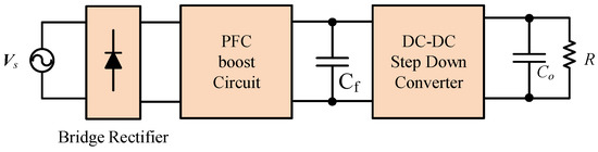
Figure 1.
Two-stage AC/DC conversion structure.
Step-down PFC rectifiers, such as buck converters are therefore considered. However, the buck rectifier input current is discontinuous. A dead angle also exists when the line input voltage is lower than the output voltage so that the input current cannot be easily shaped [6,7,8]. As a result, the step up/down AC-DC topologies are developed including buck-boost, Cuk, and Sepic type rectifiers [9,10,11]. The buck-boost rectifier also has inherent discontinuous input current like the buck converter, and needs an additional filter to smooth the input current. Although the Sepic rectifier has continuous input current, the output current is still discontinuous and easily causes output voltage ripples.
Bridgeless rectifier topologies are explored in [12,13] to reduce the diode bridge conduction losses and increase the conversion efficiency. The bridgeless PFC boost rectifiers, such as the dual boost rectifier and the totem-pole boost rectifier, have been discussed [14]. Due to the need for lower output voltage applications, the bridgeless Cuk/Sepic rectifiers [15,16] with two dc/dc Cuk/Sepic circuit structures were proposed. The bridgeless Cuk rectifier [16] is shown in Figure 2. However, four diodes are still needed to achieve step up/down output voltage. Other bridgeless Sepic [17] and Cuk [18] power-factor-correction rectifiers were also proposed with reduced number of components and conduction losses. These rectifiers were operated in discontinuous conduction mode without current loop control. A control method for bridgeless Cuk/Sepic power factor correction rectifier operated in continuous conduction mode was also proposed to achieve power decoupling [19]. Although, the bulky electrolytic capacitor can be replaced with a small film capacitor, this control method requires an extra voltage sensor for the intermediate capacitor and the system cost is increased.
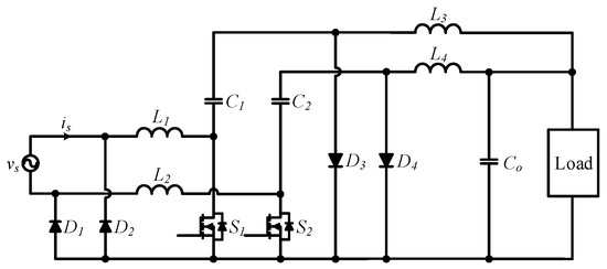
Figure 2.
Bridgeless Cuk rectifier [16].
Pulsating power buffering technology [8,20,21] has recently expanded, which can reduce the number of components including passive and active ones. Although rectifiers using pulsating power buffering technology have high power density, high conversion efficiency and high reliability, high voltage stress is still present in the switches and diodes [22], which leads to high switching and conduction losses and reduces the rectifier life-span.
This paper proposes a bridgeless Cuk rectifier with modified dual loop control scheme. The voltage stresses in the switches and diodes can be adjusted to low voltage levels by the proposed control scheme, which may reduce the switching and conduction losses and increase the rectifier life-span. The detailed operation principle and switching sequence of the bridgeless Cuk rectifier are explained. Simultaneously, a modified dual loop control scheme is also proposed to achieve input current shaping and output voltage regulation as well as voltage stress reduction.
2. Circuit Topology and Switching Sequence
The bridgeless Cuk converter [19] discussed in this paper is shown in Figure 3. The proposed control switching sequence and key waveforms in one switching period during the positive and negative half line cycle are shown in Figure 4. For convenience of discussion the active switches are assumed to be ideal active switches with anti-paralleling body diode. Both the input inductor Ls and output inductor Lo are assumed to be operated in continuous conduction mode. The circuit operation can be divided into three operation states in one switching period T for both positive and negative half-line cycles. The circuit operation principle of the bridgeless Cuk converter during the positive half-line cycle is discussed first, as follows:
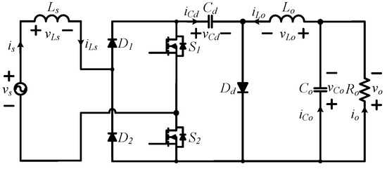
Figure 3.
Bridgeless Cuk converter [19].
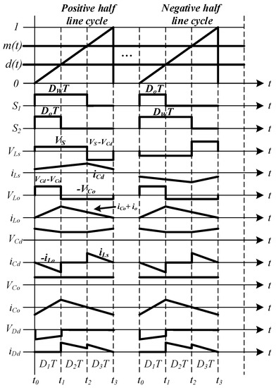
Figure 4.
Control switching sequence and key waveforms in one switching period.
(1) State 1 (t0 ≤ t <t1): In this state, as shown in Figure 5, both switches S1 and S2 are turned on. The zero-voltage switching of S2 is obtained due to body diode conducting in switch S2 in the pre-state, i.e., State 3. The input inductor Ls is magnetized by the input voltage Vs so as to increase the inductor current iLs. The inductor current iLs flows through diode D1 and switch S1 and goes back to the main ac source. Simultaneously, the intermediate capacitor Cd releases energy to the output inductor Lo and load. The equivalent circuit equations are described as Equations (1)–(4).
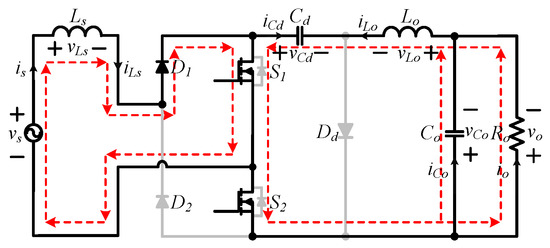
Figure 5.
Equivalent circuit of the bridgeless Cuk converter in State 1 during positive half line cycle.
(2) State 2 (t1 ≤ t <t2): In this state, as shown in Figure 6, switch S1 is turned on and switch S2 is turned off. Switch current ids1 is increasing. Input inductor Ls is still magnetized by the input voltage Vs so as to increase the inductor current iLs which still flows through diode D1 and switch S1 and then goes back to the main ac source. The voltage of intermediate capacitor Cd remains constant. Simultaneously, the output inductor Lo is demagnetized and releases energy to the load through the diode Dd. The equivalent circuit equations are expressed as Equations (5)–(8).
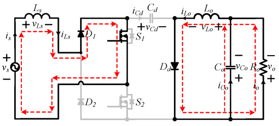
Figure 6.
Equivalent circuit of the bridgeless Cuk converter in State 2 during positive half line cycle.
(3) State 3 (t2 ≤ t <t3): In this state, as shown in Figure 7, switch S1 is turned off and S2 is also turned off. Input inductor Ls is demagnetized by the voltage −(Vcd−Vs) so as to decrease the inductor current iLs which flows through diodes D1 and Dd, and the body diode of switch S2 and goes back to the main ac source. The intermediate capacitor Cd is charged by the input inductor current iLs. Simultaneously, the output inductor Lo still releases energy to the load through diode Dd. The equivalent circuit equations are given by Equations (9)–(12).
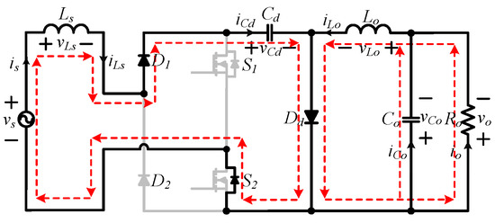
Figure 7.
Equivalent circuit of the bridgeless Cuk converter in State 3 during positive half line cycle.
Referring the gate signals shown in Figure 4, while the bridgeless Cuk converter is operated during the negative half line cycle, the circuit operation principle in the proposed control switching sequence can be described as follows:
(1) State 1 (t0 ≤ t <t1): In this state, as shown in Figure 8, both the switches S1 and S2 are turned on. The zero-voltage switching of S1 is obtained due to body diode conducting in switch S1 in the pre-state, i.e., State 3. The input inductor Ls is magnetized by the input voltage Vs so as to increase the inductor current iLs in the inverse direction. The inductor current iLs flows through diode D2 and switch S2 and goes back to the main ac source. Simultaneously, the intermediate capacitor Cd releases energy to the output inductor Lo and load. The equivalent circuit equations are described as Equations (13)–(16).
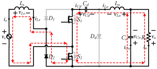
Figure 8.
Equivalent bridgeless Cuk converter circuit in State 1 during negative half line cycle.
(2) State 2 (t1 ≤ t <t2): In this state, as shown in Figure 9, switch S2 is turned on and switch S1 is turned off. The switch current ids2 is increasing. Input inductor Ls is still magnetized by the input voltage Vs so as to increase the inductor current iLs in the inverse direction which still flows through diode D2 and switch S2 and then goes back to the main ac source. The intermediate capacitor Cd voltage remains constant. Simultaneously, the output inductor Lo is demagnetized and releases energy to the load through diode Dd. The equivalent circuit equations are expressed as Equations (17)–(20).
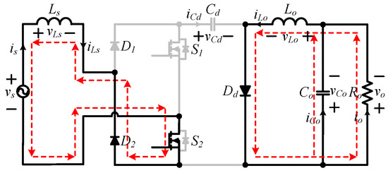
Figure 9.
Equivalent circuit of the bridgeless Cuk converter in State 2 during negative half line cycle.
(3) State 3 (t2 ≤ t <t3): In this state, as shown in Figure 10, switch S2 is turned off and S1 is also turned off. Input inductor Ls is demagnetized in the inverse direction by the voltage (Vcd + Vs) so as to decrease the inductor current iLs which flows through diodes D2, Dd and the body diode of switch S1 and goes back to the main ac source. The intermediate capacitor Cd is charged by the input inductor current iLs in the inverse direction. Simultaneously, the output inductor Lo still releases energy to the load through diode Dd. The equivalent circuit equations are given by Equations (21)–(24).
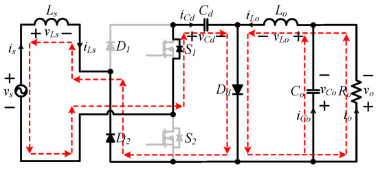
Figure 10.
Equivalent circuit of the bridgeless Cuk converter in State 3 during negative half line cycle.
To further reveal the potential merits of the proposed step up/down converter with modified dual loop control, Table 1 is provided to summarize comparisons for the bridge Cuk [11], bridgeless Cuk [16], and the proposed step up/down converter with modified dual loop control. It is worth mentioning that the power levels of the three converters in Table 1 are all at small power levels like the fly-back converter. Although the control methods may be different, the harmonics of the three converters all meet the IEC61000-3-2 Class D standard.

Table 1.
Comparisons of step up/down converters.
3. Control Scheme and Parameter Design
3.1. Control Scheme
According to the circuit analysis in the previous section, assume the duty ratio DW = D1 + D2 and D0 = D1. While the main ac voltage is operating in the positive half line cycle vs > 0, by utilizing state-space averaged technique and flux balance theory in the input inductor Ls and output inductor Lo, one can obtain the equations
Similarly, while the main ac voltage is operating in the negative half line cycle vs < 0, the corresponding symmetrical equations can also be obtained as
Merging Equations (25)–(28) in both the positive and negative half line cycles of the main ac voltage, the voltage gain of the bridgeless Cuk converter is obtained as
As can be observed from Equation (29), the output voltage is related to the two parameters Do and DW. If the input and output voltages are given, infinite different kinds of solutions exist in the Equation (29). However, in the same operation condition for the conventional dual loop control scheme shown in Figure 11, only one solution is obtained, i.e., Do = DW. Therefore, in order to reduce the voltage stresses of all switches and diodes in the circuit, the conventional dual loop control scheme is not suitable.
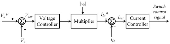
Figure 11.
Conventional dual loop control scheme.
A modified dual loop control scheme is proposed. The proposed control scheme for the bridgeless Cuk converter is shown in Figure 12. The actual input current iLs compared with the current command iLs* to generate the current error as the input of the current controller and then produce the control signal VDw. The actual output voltage Vo compared with the output voltage command Vo* generates the voltage error as the voltage controller input. The voltage controller generates the current command amplitude and also the control signal VDo. In the conventional dual loop control scheme, only one control signal is produced to achieve both input current shaping and output voltage regulation. In the proposed control scheme, two control signals VDw and VDo are produced to control the input current shaping and output voltage regulation. Thus, the intermediate capacitor voltage is not fixed and can be adjusted to fit a better low voltage level. Hence, the intermediate capacitor voltage stress could be reduced and the adopted electrolytic capacitor life span could also be increased. According to the circuit analysis in Section 2, the voltage stresses of active switches S1 and S2, diodes D1, D2, and Dd are clamped and equal to the intermediate capacitor voltage. The average switching power loss Ps in one switching period caused by transitions can be defined as
where and are the turn-on and turn-off crossover intervals, respectively. For simplification, the switches are operated in the same turn-on and turn-off crossover intervals and at the same switching frequency fs. The average switching power loss is then proportional to the voltage across the switch VDS and the entire current IDS which flows through the switch as
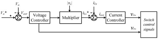
Figure 12.
Proposed modified dual loop control scheme.
According to the above equation, if the intermediate capacitor voltage is adjusted to fit a better low voltage level, the average switching power loss is also reduced. This is also true for the diodes. Therefore, the total losses in semiconductor devices can be reduced and the efficiency can be lifted.
3.2. Parameter Design
To verify the feasibility of the proposed step up/down AC/DC converter with modified dual loop control, a parameter design for inductor and capacitor is discussed. In order to find the boundary between the continuous and discontinuous modes for input inductor Ls, one can find that the critical value of K1 at boundary between modes, , is function of duty cycle Dw and can be expressed as
The critical value Kcirt (Dw) is plotted vs. duty cycle Dw in Figure 13. Consider inductor Ls is operated in CCM and the switching frequency is fs. The maximum input current ripple is less than 25% of the fundamental current. The minimum input inductor Ls value can be derived by the equation
where is the input current ripple while inductor L1 is operated in BCM. Consider that inductor Lo is operated in BCM and one can find that the critical value for K2 at the boundary between modes, , is function of the duty cycle Do and can be expressed as
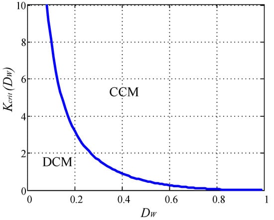
Figure 13.
Proposed step up/down AC/DC converter Kcirt (Dw) vs. Dw.
The critical value Kcirt (Do) is plotted vs. duty cycle Do in Figure 14. Similarly, the minimum value of inductor Lo also can be derived as
where is the output current ripple while inductor Lo is operated in BCM.
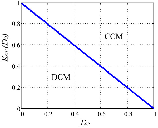
Figure 14.
Proposed step up/down AC/DC converter Kcirt (Do) vs. Do.
Consider the output capacitor and assume the switching ripple is neglected. The output capacitor must be large enough to minimize the output ripple because the output voltage ripple frequency is twice the input line frequency. The output filter capacitor can be determined by
where is the output voltage ripple and is the input line angular frequency.
4. Simulation and Experimental Results
To verify the validity of the bridgeless step up/down AC/DC converter, some simulation results are executed and a prototype system is constructed to facilitate the theoretical results as verification. The simulation and experimental parameters are listed in Table 2. The input voltage is the AC grid with 110 Vrms and 60 Hz fundamental frequency. The controlled output voltage is 48 V and the load is 48 Ω. The assigned output power rating is 48 W. The simulation results for the input voltage Vs, input current is and the corresponding intermediate capacitor voltage Vcd are shown in Figure 15. It follows from Figure 15 that the input current shaping can be achieved. Figure 16 shows the switching control signals for switch S1 and S2 and the corresponding voltage and current of switch S2 during the positive half-line cycle. As can be seen from Figure 16, the ZVS turn-on of switch S2 is obtained during the positive half-line cycle. Similarly, Figure 17 shows the switching control signals for switch S1 and S2 and the corresponding voltage and current of switch S1 during the negative half-line cycle. It also can be seen from Figure 17 that the ZVS turn-on of switch S1 is obtained during the negative half-line cycle.
Table 2.
Parameters of the bridgeless Cuk converter for simulation and experimentation.
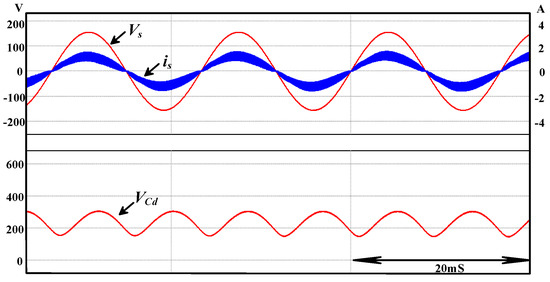
Figure 15.
Simulation results for (top) the input voltage Vs, current is, and (bottom) corresponding intermediate capacitor voltage.
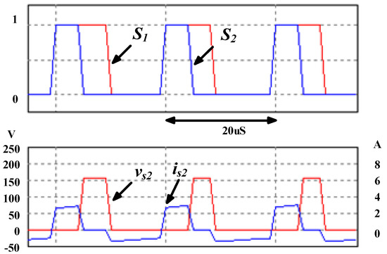
Figure 16.
Simulation results for (top) switching control signals and (bottom) corresponding voltage and current of switch S2 during positive half line cycle.
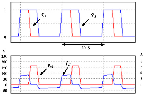
Figure 17.
Simulation results for (top) switching control signals and (bottom) corresponding voltage and current of switch S1 during negative half line cycle.
Consider that the load is a dynamic load and/or RL load such as a dc motor whose armature winding resistance is Ra = 0.5 Ω, armature winding inductance is La = 0.5 mH, back electromotive force is 47 V. Figure 18 shows the simulation results for the input voltage, input current and the corresponding intermediate capacitor voltage. As can be observed from Figure 18, the output power is about 120 W and the power factor correction is also achieved. Hence, the proposed converter can indeed be operated in the RL load. Consider the intermediate capacitor voltage which can be adjusted using the control signal VDo based on Equations (26) and (28). Figure 19 shows the simulation results for the input voltage and the corresponding input current, and the control signal VDo and the corresponding intermediate capacitor voltage VCd under the low control signal VDo value. Figure 20 shows the same simulated condition under the high control signal VDo value. It can be seen from Figure 19 and Figure 20 that the lower the control signal VDo value, the higher the intermediate capacitor voltage VCd. That the duty ratio Do affects the intermediate capacitor voltage level and also the voltage stresses of the switches and diodes in the circuit is very important information. This also implies that the duty ratio Do affects the converter power losses and efficiency. Finally, to facilitate understanding of the proposed step up/down converter with modified dual loop control and as verification, a prototype is constructed with a TMS320F28335 digital signal processor (DSP). The experimental hardware construction block diagram is shown in Figure 21. Figure 22 and Figure 23 show the experimental results for the switching control signals and the corresponding voltage and current of switches S2 and S1 during positive and negative half-line cycles, respectively. As can be observed from Figure 22 and Figure 23, the ZVS soft switching of switches S2 and S1 were indeed achieved and agreed with the simulation results. The measured harmonic distribution of the input current is shown in Figure 24. One can find that the measured harmonic currents meet the IEC 61000-3-2 Class D harmonic standards.
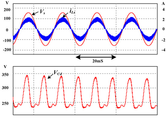
Figure 18.
Simulation results for (top) the input voltage Vs, current is, and (bottom) corresponding intermediate capacitor voltage while the load is a dc motor.
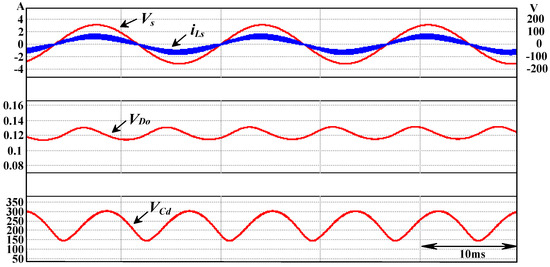
Figure 19.
Simulation results for (top) the input voltage Vs, current is, (middle) the control signal VDo with low parameter value, and (bottom) corresponding intermediate capacitor voltage.
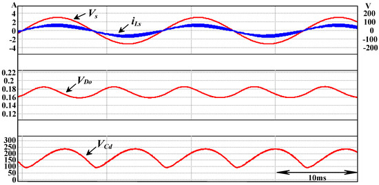
Figure 20.
Simulation results for (top) the input voltage Vs, current is, (middle) the control signal VDo with high parameter value, and (bottom) corresponding intermediate capacitor voltage.
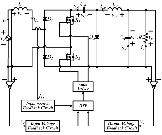
Figure 21.
Experimental hardware construction block diagram.
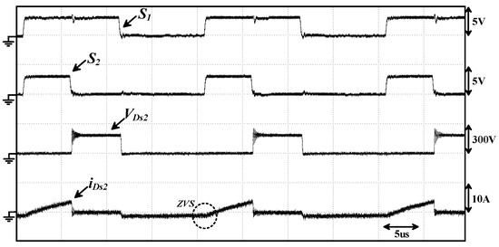
Figure 22.
Experimental results for (top) switching control signals S1, S2 and (bottom) corresponding voltage and current of switch S2 during positive half line cycle.
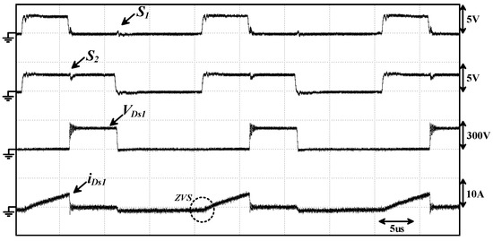
Figure 23.
Experimental results for (top) switching control signals S1, S2 and (bottom) corresponding voltage and current of switch S1 during negative half line cycle.
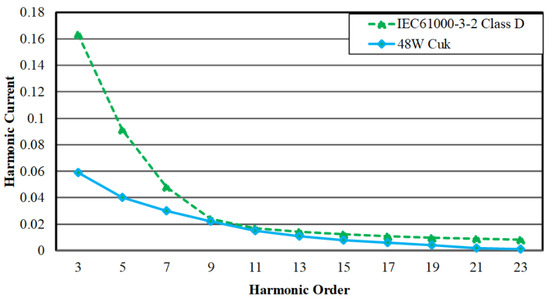
Figure 24.
The measured harmonic distribution of the input current compared with IEC61000-3-2 Class D standard.
In order to understand the total harmonic distortion THDi of the input currents in the three converters listed in Table 1, the PSIM software is adopted to carry out the simulation. The input voltage is 110Vrms, the output voltage is controlled at 48 V and the load is 2 A. The corresponding parameters and simulated results are shown in Table 3. As can be seen from Table 3, the input current THDi of the bridge Cuk [11] is better than that of the bridgeless Cuk [16] and the proposed Cuk with modified dual loop control scheme. Nevertheless, the parameter value of the bridge Cuk input inductor [11] is larger than those for the other two. Although the bridge Cuk [11] has the smallest input current THDi, the input inductor may make it appear bulky.
Table 3.
Comparisons of the total harmonic distortion of the step up/down converters.
5. Conclusions
This paper presented a bridgeless step up/down converter with modified dual loop control scheme. The proposed system has ZVS soft switching in switches S1 and S2 during the negative and positive half-line cycle operation, respectively. Thus, the switching losses can be reduced and the thermal stress can be balanced between switches S1 and S2. There are fewer components compared to the bridge Cuk and the bridgeless dual Cuk configuration. Therefore, the size and cost can be reduced. In addition, based on the proposed control scheme, the voltage stresses of the intermediate capacitor, active switches, and diodes can all be reduced. To verify the validity of the proposed step up/down converter, simulation, and experimental results are offered. From simulation and experimental results, the proposed bridgeless step up/down converter can indeed achieve input current shaping and output voltage regulation as well as reduce the switching and conduction losses.
Author Contributions
The author contributed to the theoretical analysis, modeling, simulation, experiment, and manuscript preparation. The author have read and agreed to the published version of the manuscript.
Funding
This research is sponsored by the Ministry of Science and Technology of R.O.C. under grant MOST 108-3116-F-008-001.
Conflicts of Interest
The authors declare no conflict of interest.
References
- Bodetto, M.; El Aroudi, A.; Cid-Pastor, A.; Calvente, J.; Martinez-Salamero, L. Design of ac–dc PFC high-order converters with regulated output current for low-power applications. IEEE Trans. Power Electron. 2016, 31, 2012–2025. [Google Scholar] [CrossRef]
- Chang, C.H.; Cheng, C.A.; Chang, E.C.; Cheng, H.L.; Yang, B.E. An integrated high-power-factor converter with ZVS transition. IEEE Trans. Power Electron. 2016, 31, 2362–2371. [Google Scholar] [CrossRef]
- Kim, J.S.; Lee, S.H.; Cha, W.J.; Kwon, B.H. High-Efficiency Bridgeless Three-Level Power Factor Correction Rectifier. IEEE Trans. Ind. Electron. 2017, 64, 1130–1136. [Google Scholar] [CrossRef]
- Dusmez, S.; Choudhury, S.; Bhardwaj, M.; Akin, B. A Modified Dual-Output Interleaved PFC Converter Using Single Negative Rail Current Sense for Server Power Systems. IEEE Trans. Power Electron. 2014, 29, 5116–5123. [Google Scholar] [CrossRef]
- Li, Y.C.; Lee, F.C.; Li, Q.; Huang, X.; Liu, Z. A novel AC-to-DC adaptor with ultra-high power density and efficiency. In Proceedings of the 2016 IEEE APEC Conference and Exposition, Long Beach, CA, USA, 20–24 March 2016. [Google Scholar]
- Jang, Y.; Jovanović, M.M. Bridgeless buck PFC rectifier. In Proceedings of the 2010 IEEE APEC Conference and Exposition, Palm Springs, CA, USA, 21–25 February 2010. [Google Scholar]
- Huber, L.; Gang, L.; Jovanovic, M.M. Design-Oriented Analysis and Performance Evaluation of Buck PFC Front End. IEEE Trans. Power Electron. 2010, 25, 85–94. [Google Scholar] [CrossRef]
- Ohnuma, Y.; Itoh, J.I. A Novel Single-Phase Buck PFC AC-DC Converter with Power Decoupling Capability Using an Active Buffer. IEEE Trans. Ind. Appl. 2014, 50, 1905–1914. [Google Scholar] [CrossRef]
- Firnao Pires, V.; Fernando Silva, J. Half-bridge single-phase buck-boost type AC-DC converter with sliding-mode control of the input source current. IEE Proc. Electr. Power Appl. 2000, 147, 61–67. [Google Scholar] [CrossRef]
- Abdelsalam, I.; Adam, G.P.; Holliday, D.; Williams, B.W. Single-stage, single-phase, ac–dc buck–boost converter for low-voltage applications. IET Power Electron. 2014, 7, 2496–2505. [Google Scholar] [CrossRef]
- Simonetti, D.S.L.; Sebastian, J.; Uceda, J. The discontinuous conduction mode Sepic and Cuk power factor preregulators: Analysis and design. IEEE Trans. Power Electron. 1997, 44, 630–637. [Google Scholar] [CrossRef]
- Mitchell, D.M. AC-DC Converter Having an Improved Power Factor. U.S. Patent 4,412,277, 25 October 1983. [Google Scholar]
- Choi, W.Y.; Kwon, J.M.; Kim, E.H.; Lee, J.J.; Kwon, B.H. Bridgeless boost rectifier with low conduction losses and reduced diode reverse-recovery problems. IEEE Trans. Ind. Electron. 2007, 54, 769–780. [Google Scholar] [CrossRef]
- Huber, L.; Jang, Y.; Jovanovic, M.M. Performance evaluation of bridgeless PFC boost rectifiers. IEEE Trans. Power Electron. 2008, 23, 1381–1390. [Google Scholar] [CrossRef]
- Sabzali, A.J.; Ismail, E.H.; Al-Saffar, M.A.; Fardoun, A.A. New Bridgeless DCM Sepic and Cuk PFC Rectifiers with Low Conduction and Switching Losses. IEEE Trans. Ind. Appl. 2011, 47, 873–881. [Google Scholar] [CrossRef]
- Fardoun, A.A.; Ismail, E.H.; Sabzali, A.J.; Al-Saffar, M.A. New Efficient Bridgeless Cuk Rectifiers for PFC Applications. IEEE Trans. Power Electron. 2012, 27, 3292–3301. [Google Scholar] [CrossRef]
- Mahdavi, M.; Farzanehfard, H. Bridgeless SEPIC PFC Rectifier with Reduced Components and Conduction Losses. IEEE Trans. Ind. Electron. 2011, 58, 4153–4160. [Google Scholar] [CrossRef]
- Mahdavi, M.; Farzaneh-Fard, H. Bridgeless CUK power factor correction rectifier with reduced conduction losses. IET Power Electron. 2012, 5, 1733–1740. [Google Scholar] [CrossRef]
- Liu, Y.; Sun, Y.; Su, M. A Control Method for Bridgeless Cuk/Sepic PFC Rectifier to Achieve Power Decoupling. IEEE Trans. Ind. Electron. 2017, 64, 7272–7276. [Google Scholar] [CrossRef]
- Wang, H.; Chung, H.S.H.; Liu, W. Use of a series voltage compensator for reduction of the dc-link capacitance in a capacitor-supported system. IEEE Trans. Power Electron. 2014, 29, 1163–1175. [Google Scholar] [CrossRef]
- Qin, S.; Lei, Y.; Barth, C.; Liu, W.C.; Pilawa-Podgurski, R.C.N. A high power density series-stacked energy buffer for power pulsation decoupling in single-phase converters. IEEE Trans. Power Electron. 2017, 32, 4905–4924. [Google Scholar] [CrossRef]
- Qi, W.; Li, S.; Yuan, H.; Tan, S.; Hui, S. High-Power-Density Single-Phase Three-Level Flying-Capacitor Buck PFC Rectifier. IEEE Trans. Power Electron. 2019, 34, 10833–10844. [Google Scholar] [CrossRef]


© 2020 by the author. Licensee MDPI, Basel, Switzerland. This article is an open access article distributed under the terms and conditions of the Creative Commons Attribution (CC BY) license (http://creativecommons.org/licenses/by/4.0/).