Article

Asymmetrical Three-Level Inverter SiC-Based Topology for High Performance Shunt Active Power Filter

by
Rodrigo Guzman Iturra
* and
Peter Thiemann
Laboratory for Electrical Machines, Drives and Power Electronics, South Westphalia University of Applied Sciences (FH-SWF), 59494 Soest, Germany
*
Author to whom correspondence should be addressed.
Energies 2020, 13(1), 141; https://doi.org/10.3390/en13010141
Submission received: 10 October 2019 / Revised: 11 December 2019 / Accepted: 24 December 2019 / Published: 27 December 2019
(This article belongs to the Special Issue Power Electronics for Smart Grids: Present and Future Perspectives)

Abstract

:
Power quality conditioner systems, such as shunt active power filters (SAPFs), are typically required to have low power losses, high-power density, and to produce no electromagnetic interference to other devices connected to the grid. At the present, power converters with such a features are built using multilevel topologies based on pure silicon semiconductors. However, recently new semiconductors that offer massive reduction of power losses such as silicon carbide (SiC) MOSFETs have been introduced into the power electronics field. In the near future, the applications that demand the highest performance will be powered by multilevel converters based on SiC. In this paper a highly efficient three-level (3L) topology based entirely on silicon carbide (SiC) semiconductors for a SAPF is presented and analyzed in great detail. Furthermore, the proposed topology is compared with other full SiC-based conventional topologies: two level (2L), three-level T-type (3L-TNPC), and three-level neutral-point-clamped (3L-NPC) in terms of efficiency. The proposed asymmetrical topology has an efficiency superior to conventional all SiC 2L and 3L power circuits when the pulse or switching frequency of the system is set higher than 60 kHz. Further, for high current ratings, the asymmetrical topology has the advantage that it can be built just by cascading two half-bridge SiC modules.

1. Introduction

The work presented in this research article is an expanded and extended version of the conference paper [1].
Numerous and complex challenges are imposed on power systems at present times: a steady increasing energy demand in industrial and residential applications [2,3,4], the integration of renewable energies systems (RESs) and distributed generation (DG) [5,6,7] and the assurance of high power quality [8,9] and reliability [10] in face of the highly reconfigurable and extremely dynamic nature that power grids are acquiring due to rapid changes in loads and power sources. The way to tackle the mentioned challenges is a more intelligent power grid or smart grid. Such smart grids should allow the full use of renewables, be highly flexible, and have reliable and high power capable to cope with the increasing energy demands [2,5]. Advances in many technologies are needed for the realization of the smart grid, advances in the areas of power systems, power electronics, information and communications [11], and artificial intelligence [12,13]. Moreover, it is important to emphasize the pivotal role that power electronics technologies play in smart grids. First, static power converters based on power electronics are fundamental and indispensable elements to interface RESs power sources, such as solar photovoltaic arrays (PV), wind turbines, and batteries, with the power grid. Static converters transform the raw power produced by clean energy sources into electrical power in a form that is suitable to be stored (e.g., in batteries) or to be injected into the grid [2,5,14]. Second, power electronics technologies are the enablers for the efficient conversion and control of the electrical power in modern electrical loads such as computers, lighting devices, adjustable speed drives (ASDs), and uninterruptible power supplies (UPS), among other applications [15,16]. Modern fully controllable loads will be key in the future supply-demand interactive energy management systems of the future smart grid. As supply has to match the load demand and RESs produce inherently power in a fluctuating manner due to their dependency to weather conditions, “smart loads” that shut down at peak hours and turn on when there is a surplus of renewable power generation, will become necessary for an optimum supply of electricity to final users [17].
Static power converters are vital for smart grids; however, these power electronics-based devices produce some negative and adverse effects on the power grid. Power converters are based on switching mode operation, in consequence their voltage/current characteristic is nonlinear [8,15,18]. In other words, these devices draw currents with a high harmonic content even when they are connected to a power system that supplies pure sinusoidal voltages with a fundamental frequency of 50 Hz or 60 Hz. The currents drawn can be either highly discontinuous as in the case of loads fed by three phase diode rectifiers which produce low frequency harmonics at integer multiples of the fundamental frequency [19], or the currents drawn can have a harmonic content related with the switching frequency operation of the power converters as is the case of photovoltaic grid inverters [20]. Harmonic currents drawn by power converters create harmonic voltage distortion due to the harmonic voltage drop provoked by the currents in the equivalent impedance of the power grid. Harmonic voltage distortion degrades the efficiency of the power system and also leads to heating and malfunctioning of electrical devices connected [15,16,18]. The voltage distortion levels and frequency have to be maintained within certain limits in order to guarantee a high power quality and reliability in the smart grid.
State-of-the-art solutions to combat power quality problems such a harmonic voltage distortion are shunt active power filters (SAPFs) of the voltage source converter (VSC) type [16]. An example of such solution is depicted in Figure 1. Power quality conditioner systems such as SAPFs are typically required to have low power losses, high power density, and to produce no electromagnetic interference to other devices connected to the grid. To fulfill such demanding requirements, modern SAPF solutions are form by silicon semiconductors (IGBTs and diodes) in multilevel power circuit structures. Voltage source multilevel converters feature lower switching losses and smaller AC filters with lower losses than solutions based on two-level (2L) silicon-based VSC power circuits [21,22,23]. Recently, however, new technologies in the form of wide band gap (WBG) semiconductors have stepped in and particularly for high power and high voltage applications (above 600 V) the most suitable WBG semiconductors are SiC MOSFETs [24]. From the switching performance perspective, SiC MOSFETs outperform silicon IGBTs counterparts; this is because SiC exhibits a higher electron saturated velocity than silicon and that SiC MOSFETs are unipolar devices, and thus they have no stored charges that limit the switching speed. Therefore, it is possible to use SiC MOSFETs in power converters with a high switching frequency without suffering from significant switching losses [25]. The consequence is that full SiC MOSFET 2L converters operating at high switching frequency display an efficiency that is comparable or superior to multilevel pure silicon-based power converters [23,25]. Certainly, the combination of multilevel circuit structures and SiC MOSFETs will produce solutions with the highest efficiency and the highest power density. This trend will be seen in the close future for applications requiring the highest performance.
In a previous paper, we proposed a three-level (3L) non-conventional topology fully based on SiC MOSFETs with the aim of maximize the SAPF’s efficiency [1]. The proposed topology has an efficiency superior to conventional all SiC 2L (see Figure 2a) and 3L topologies (see Figure 2b,c) when the pulse or switching frequency of the system is set higher than 60 kHz, with the efficiency at full load peaking at 70 kHz. Previous works [26,27,28] studied the non-conventional topology based on pure silicon semiconductors (IGBTs and diodes) in three-phase PFC rectifiers and single SAPFs. The focus was on the design of current control loops, DC-Bus voltage balancing and fully digital control implementation. Furthermore, only Reference [26] analyzed the switching states of the topology but just for the single phase PFC IGBT Si case. This paper comes to extend our previous paper [1] by analyzing in detail the switching states of the proposed topology and current commutations during switching states transitions that are indeed very different to the ones seen in the topology with silicon IGBTs due to the third quadrant characteristic of SiC MOSFET devices. Moreover, this paper includes a profound discussion of the topology power losses, topology’s efficiency, and a detailed losses comparison with the 2L and conventional 3L full SiC-based solutions that has not been done in our previous work. The paper is organized as follows. In Section 2, the fundamental working principles of the SAPF are highlighted. In Section 3, the main characteristics of the proposed topology are presented and discussed in great detail. In Section 4, a discussion about the losses performed by the topologies based on simulation results is carried out. In Section 5, experimental results are shown in order to demonstrate the feasibility of the solution. Finally, in Section 6, the conclusions are performed.

2. Shunt Active Power Filter-Based on Voltage Detection (VSAPF)

2.1. VSAPF Fundamental Principles

A SAPF can be conceived as a controlled current source that injects compensating currents IC into the power system (see Figure 1). There are three main control methodologies to generate the reference for the compensating currents: load current detection, supply current detection, and voltage detection [29]. For the methods load current detection and supply current detection the compensating currents IC injected by the SAPF are proportional either to the harmonic load current ILh or to the harmonic supply current ISh. In both of these methods, the SAPF measures currents in order to generate the references for the compensating currents IC. A voltage based SAPF (VSAPF) works differently, it measures the voltage at the point of common coupling (PCC), extracts the harmonic content and injects currents that are proportional and in phase to the measured harmonic voltages. It does not measure any current from the load or from the supply side. This is the reason why industrial applications of VSAPFs are often known sensorless controlled SAPFs. In this paper, we focus on the voltage detection control strategy that is explained in great detail by Akagi in [30]. If this control strategy is implemented, the VSAPF behaves as a resistor at harmonic frequencies and therefore can be used to damp out resonances that arise due to the interaction of inductors and capacitors in the power system. In presence of nonlinear loads, the voltage at the PCC consists of a fundamental component v1 and harmonic voltages at different frequencies. In a three-wire three phase system, the typical harmonics are the 5th, 7th, 11th, 13th, and many others that correspond to the harmonic voltages v5, v7, v11, v13 and others. The sum of all the harmonic voltages together can be represented by the term vh. If we establish ω = 2 π f1 as the fundamental frequency, and take the voltage phase angle at the fundamental frequency at the PCC as reference α 1 = 0, the voltage at the PCC can be mathematically described by the following equation [31],
v PCC ( t ) = v 1 ( t ) + v h ( t )
v h ( t ) = v 2 ( t ) + v 3 ( t ) + = h = 2 h = 2 V h s i n ( h ω t - α h )
where the phase shift between the voltage at harmonic frequency h with respect to the phase angle taken as reference is α h . A VSAPF injects compensating currents at harmonic frequencies iCh proportional and in phase to harmonic voltages at the PCC. Moreover, a current at the fundamental frequency is also drawn by the VSAPF that is used to regulate the DC bus voltage iC1. Altogether, it follows that the compensating currents injected by the VSAPF can be expressed as
i C ( t ) = i C 1 ( t ) + i Ch ( t )
with:
i Ch ( t ) = i C 2 ( t ) + i C 3 ( t ) + = h = 2 h = 2 I h s i n ( h ω t - β h )
where the phase shift between the voltage at harmonic frequency h with respect to the phase reference α 1 is β h . The VSAPF control law, defined by Akagi in [30], states that to emulate a resistance at harmonic frequencies, the harmonic compensating currents iCh need to be in phase to the existent harmonic voltages at the PCC, it follows that
α h β h
for each harmonic frequency h > 1. It is possible to define the phase difference θh between the harmonic component of voltage and current waveform of order h. If harmonic voltages and currents are in phase then the phase difference will tend to be zero. It can be expressed as
θ h = α h - β h 0
Furthermore, the control law also establish that the harmonic compensating currents need to be proportional to the harmonic voltages, therefore it follows that
I h = V h R s
where the proportionality factor between harmonic voltages and currents is 1 R s . Thus, the VSAPF forms a closed loop between Vh and Ih, and it behaves fundamentally as a shunt virtual harmonic resistor of Rs( Ω ) connected in parallel to the grid. The damping provided by the virtual resistor avoids the amplification of harmonic voltages and currents due to resonance conditions. In other words, harmonic resonances are suppressed by the VSAPF. Moreover, if the virtual resistor impedance is set smaller than the equivalent impedance of the power network, the harmonic currents generated by nonlinear loads will be confined to flow through the VSAPF and will not penetrate into the power system, leading to a voltage Total Harmonic Distortion (THD) reduction at the PCC. The fundamental component of the compensating currents iC1 determines the amount of active power at the fundamental frequency that will be exchanged with the power grid.

2.2. VSAPF Control System

The VSAPF control system is depicted in Figure 3. It has four main parts: two outer loops, one inner current control loop, and one DC-side voltage equalizer. The first outer loop is the one in charge to generate the reference for the harmonic content of the compensating currents. First, the first outer loop senses the grid voltages vPCC and then extracts the harmonic content vh of each phase through signal processing over the vPCC signals. The mentioned process removes the fundamental component v1 from vPCC. Afterwards, vh is scaled by the reciprocal of the target virtual resistance Rs to generate the reference i*Ch. As the VSAPF is meant to operate with a self-supporting DC-Bus, a second outer loop is designed to maintain the voltage of the DC-Bus to a constant level. Depending on whether the DC-bus voltage is below or above its reference, the second outer loop sets the reference for the fundamental current iC1 to absorb/release fundamental active power from/to the power system [29]. The third component of the system is the inner current control loop. The former determines the appropriate modulation reference to be fed into the pulse width modulator (PWM) such that the VSC synthesizes the compensating currents matching the reference i*C = i*C1 + i*Ch. In this work, the current controller design is based largely on [32]. Finally, as all the 3L converters in this study are realized with a DC-side voltage divider (two capacitors in series in the DC-bus), the capacitors on the DC-bus are subject to suffer of the partial DC-side voltage drift phenomenon where the voltage of both of the capacitors becomes unbalanced [33,34]. Therefore, a DC-side voltage equalizer becomes necessary to maintain the voltage of both of the DC-Bus capacitors symmetrical.

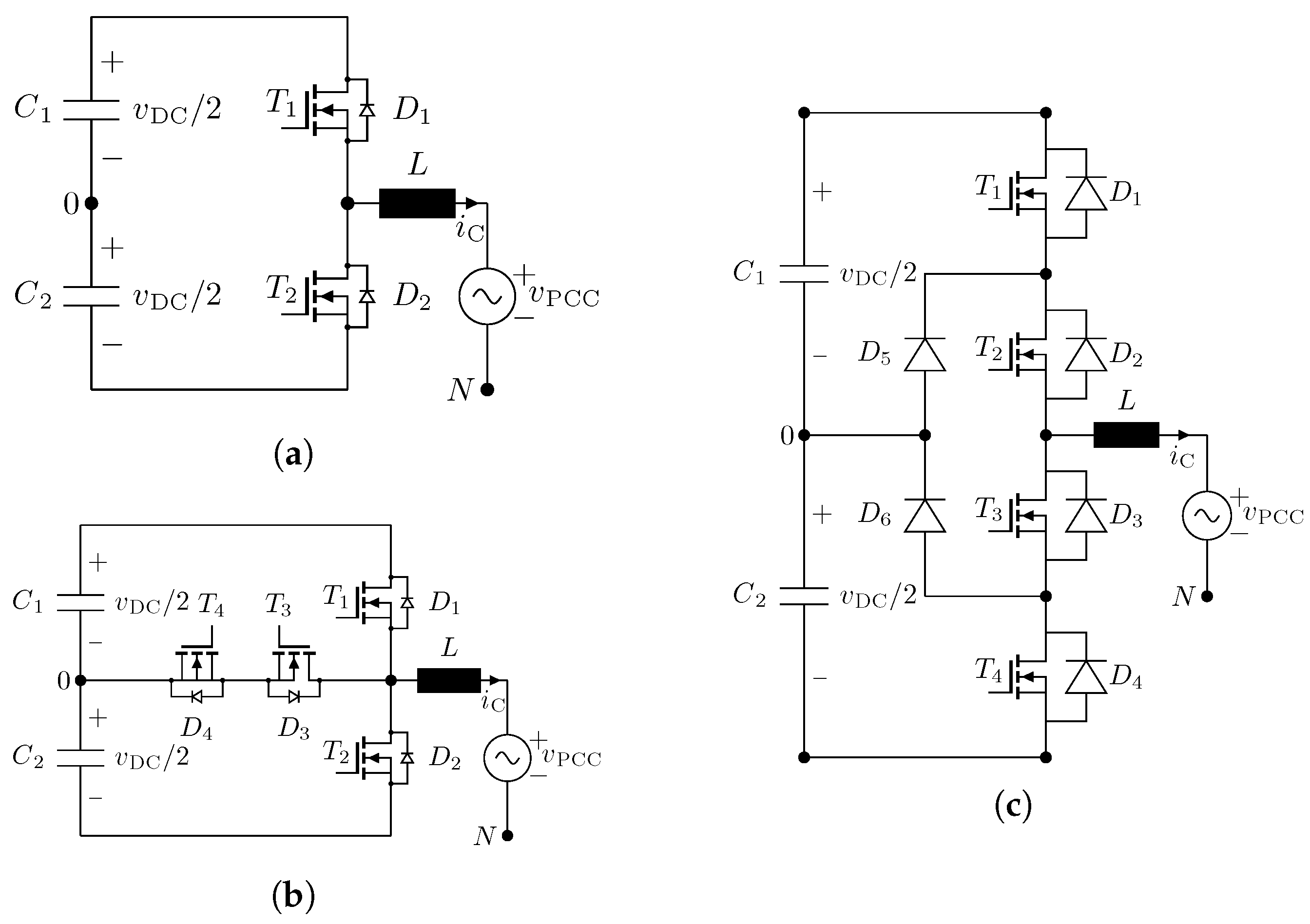
3. Asymmetrical Three Level Converter Topology (3L-ASYM)

Figure 4 shows one leg of the three phase 3L nonconventional topology proposed as power circuit for the VSAPF. The non-conventional topology is named is this paper as asymmetrical three-level converter 3L-ASYM for reasons that will become clear at Section 3.2. In the figure, it can be seen that two capacitors in series hold the DC-Bus voltage and that the neutral point is located in the middle point of both capacitors. Furthermore the switches T1-T4 are selected to be SiC MOSFETs and the diodes D1-D4 are selected to be SiC Schottky barrier diodes (SBD). The proposed nonconventional topology has the main advantage that its design is based on two power electronics building blocks, in this case a pair of two level commutation cells in a cascade connection. In other words, the proposed topology can be built just with two half bridge SiC MOSFETs modules connected in a cascaded connection, connecting the AC terminal of one module to the positive terminal of the second module.

3.1. Switching States

The neutral point 0 is taken as the reference node for the incoming analysis. In consequence, the potential of the positive rail p becomes vDC/2 and the potential of the negative rail n becomes –vDC/2. The voltage vo is defined as the output voltage. If T1 and T3 are switched ON, the output voltage takes the vDC/2 potential. At the mentioned switching state, the voltage stress across T2 is half of the DC-Bus voltage (vDC/2) and the stress across T4 is the full DC-Bus voltage (vDC). If T2 and T3 are ON, the output voltage takes the 0 potential. The voltage stress across T1 is half of the DC-Bus voltage vDC/2 and the stress across T4 is also vDC/2. If T2 and T4 are ON and T3 is OFF, the output voltage assumes –vDC/2 potential. The voltage stress across T1 is half of the DC-Bus voltage vDC/2 and the stress across T3 is also vDC/2. All the switching states of the VSAPF proposed topology can be seen in Table 1 and a summary of the voltage stress on the different switches can be seen in Table 2. The immediate consequence of Table 2 is that switches T1, T2, T3, D1, D2, and D3 have to be selected just to block half of the DC-Bus voltage. In contrast, T4 and D4 have to be rated to sustain the complete DC-Bus voltage. Moreover, when the switch T1 is ON, it is absolutely mandatory that the switch T2 is OFF; otherwise, shoot-through occurs in the capacitor C1. Likewise, when the switch T2 is ON, it becomes necessary to command the switch T1 to OFF state. Therefore when T1 and T2 are commanded to change their states, a blanking time should be introduced as in a typical half-bridge. In essence, the previously stated applies as well also for the switches T3 and T4 to avoid shoot-through of the capacitor C2. The non-conventional topology can be driven by the level-shifted PWM modulation the same as the 3L-TNPC and 3L-NPC. In this variant, the modulating signal (Mod) is compared with two high frequency triangular waveforms (Vtri1 and Vtri2). Figure 5 shows the behavior of the PWM generation when the modulating signal is pure sinusoidal. The switches T1 and T2 change their states during the positive semicycle of the modulating signal. Also, during the positive part of the modulating signal, the switch T3 is continuously on. During the negative semicycle of the modulating signal, the switches T3 and T4 change their states and the switch T2 is continuously on.

3.2. 3L ASYM—Voltage Level Generation and Output Current

For the given topology, it is important to ensure that any desired output voltage (vDC/2, 0, –vDC/2) can be generated for positive and negative currents. In other words, irrespective of the direction of the current, it should be possible to select any of the three levels at the output port. For example, for IC > 0, to connect the AC output port (vo) of the converter to vDC/2, the semiconductors T1 and T3 conduct the current (see Figure 6). To achieve 0 in the AC output port for IC > 0, the semiconductors T2, D2, and T3 conduct the current. In contrast to connect the ac output port to –vDC/2 for IC > 0 the semiconductors T4 and D4 carry the current. The proposed non-conventional topology is named in this paper as asymmetrical three-level converter topology (3L-ASYM). The reason behind this name is the asymmetry on the number of semiconductors carrying the current at different output voltage levels. The details of the current passing to each of the semiconductors in the different converter states will be discussed in the following subsections.

3.2.1. 3L ASYM Commutation p-0 for Positive Current

Figure 6 shows the transition between 0-p for a positive current (IC > 0). During the switching state 0, the positive current flows out of the neutral point 0 through the diode D2, the transistor T2 and the transistor T3. In this switching state, the channel of T2 is open and allows a reverse current (current flow from source to drain) to pass through the SiC MOSFET switch T2. This conduction mode is called third quadrant operation of the SiC MOSFET [35] (operation similar to a synchronous rectifier [36]). Moreover, the current IC will be distributed between the SiC MOSFET T2 and the SBD diode D2. The current distribution will depend on the ON resistance (RDS) of the MOSFET, the forward voltage drop of the SiC SBD diode (VF) and the diode dynamic resistance (RF) [37]. Indeed the described switching operation is very different from what is seen in the 3L silicon-based topology. The voltage blocked by T1, D1, T4, and D4 at this state is vDC/2. During the blanking time interval between T1 and T2, the current passes entirely through the diode D2 and the transistor T3. Then, the converter is brought to the switching state p by turning the switch T1 ON. The current conmutates from D2 to T1. At this stage, T2 and D2 block half of the DC-bus voltage, and the semiconductors T4 and D4 block the full DC-Bus voltage. SiC SBDs exhibit almost zero reverse current [38], which means that the increase in switching losses due to the current commutation from Dx to Tx can be neglected at all times.

3.2.2. 3L ASYM Commutation p-0 for Negative Current

Figure 7 shows the transition 0-p for a negative compensating current (IC < 0). At the switching state 0, the current flows through T2 and through T3 and D3. The former two share the compensating current as T3 operates in third quadrant. The devices T1, D1, T4, and D4 block half of the DC-Bus voltage. During the blanking time between T1 and T2, the diode D1 conducts the current alongside with T3 and D3. T2 and D2 hold the half of the DC-Bus voltage. In contrast, T4 and D4 sustain the complete DC-Bus voltage. Finally, once the blanking time has elapsed and the transistor T1 is fully ON, the current passes through T1, D1, T3, and D3, with T1 and T3 in third quadrant operation. The devices T2, D2, T4, and D4 block the same voltage as previously stated. At this stage, the transistor T1 is turn on at almost Zero Voltage Switching (ZVS) [39,40]. This comes inherently because diode D1 is conducting the current since the beginning of the blanking time interval, thus the effective blocking voltage at the time of the switching ON transition of T1 is just the voltage drop produced by IC over D1 which is remarkable smaller than half of the DC-Bus voltage. It is possible to say that T1 is turned on partially at soft-switching and this comes inherently due to the circuit nature. There is no need of a special control loop or further control considerations to achieve partial soft-switching.

3.2.3. 3L ASYM Commutation n-0 for Positive Current

Figure 8 presents the transition 0-n for a positive compensating current (IC > 0). The semiconductors behavior for state 0 is the same as the one described in Section 3.2.1. During the blanking time interval between T3 and T4, the current conmutates from T2/D2 to the diode D4. As T2 is in conduction stated, T1, D1, and T4 block just half of the DC-Bus voltage. Finally, the conmutation concludes by turning T4 ON almost at ZVS. As this point, T4 operates in third quadrant and IC is shared between T4 and D4. T1, D1, and T4 block the same voltage as in the blanking time interval.

3.2.4. 3L ASYM Commutation n-0 for Negative Current

Figure 9 depicts the behavior of the n-0 transition for IC < 0. The switching state 0 transition is identical to the 0 state described in Section 3.2.2. All along the blanking time interval between T3 and T4 IC flows across T2 and D3. T1, D1, T4, and D4 block just half of the DC-Bus voltage. In the final stage of the transition, the switch T4 is switched ON and the current conmutates from D3 to T4. As T2 is in conduction state, T1, D1, T3, D3, and D4 block just half of the DC-Bus voltage.

4. Comparative Evaluation

SiC semiconductors offer the possibility to reduce drastically power losses due to lower switching losses, almost no reverse recovery, lower ON resistance (RDS) and lower gate charge in comparison with their pure silicon counterparts [41]. However, to benefit from the SiC devices features at the system level, the power losses of the overall system (semiconductors, inductors, ripple filter, etc.) need to be considered. At the system level, there are many degrees of freedom for the design such as circuit topology, modulation scheme, current ripple on the inductors, switching frequency, etc. Likewise, many degrees of freedom are encounter also for the components selection (core material for the inductors, solid, or litz wire for the inductor windings, semiconductors, etc.). For evaluation and comparison purposes, a three-phase VSAPF with a power rating of 23.1 kVA was designed and simulated in our previous paper [1]. The simulation software used for the power circuit, control system, thermal, and power converter losses estimation is Simulink-PLECS. GeckoMagnetics is used to calculate the power losses on the coupling inductors. The input given to GeckoMagnetics is the coupling inductor current spectrum obtained from the Simulink-PLECS simulation in order to have the same operating point in both simulation tools. The VSAPF was implemented using the topologies 2L, 3L-TNPC, 3L-NPC, and 3L-ASYM considering a DC-bus voltage vDC of 750 V. The semiconductors considered are the discrete SiC MOSFETs and SiC Schottky diodes that can be seen at Table 3. Furthermore the PLECS models of all these semiconductors were gathered from the official website of the manufacturer Wolfspeed [42]. On the other hand, the criteria to design the coupling inductors is to mantain a maximum current ripple constant in all designs. If the maximum ripple is defined as Δ I pp , then the minimum inductance necessary to achieved Δ I pp in a 2L converter can be calculated as follows [43],
L 2 L = v D C 8 · F s · Δ I pp
where Fs is the switching frequency of the converter. The last equation implies that the inductance on the coupling inductor decreases as the switching frequency is increased. Moreover, if a 3L converter is designed in such a way that the same maximum current ripple Δ I pp than in a 2L converter is to be obtained, the following applies [44],
L 3 L = 2 · L 2 L 3
The maximum current ripple was fix at 20% of the rated current Δ I pp = I n · ( 20 % ) · 2 = 13 . 4 A , and the switching frequency of the power converter was used as system design parameter to maximize the overall efficiency of the VSAPF. The topologies were compared at different switching frequencies between 10 and 120 kHz. Therefore, the coupling inductors were designed according to the Equations (8) and (9) in such a way that the maximum ripple was maintained at 13.4 A for all the 2L and 3L converters designs. The results can be seen in Figure 10a. The volume of the inductors designed through this process were calculated with the GeckoMagnetics software and the results can be seen at Figure 10b.

4.1. Simulation Results

An industrial distribution system similar to the one depicted in Figure 1 was simulated with the parameters stated in Table 4. On the scenario simulated, there is a resonance condition produced by the capacitors of a capacitor bank for reactive power compensation connected to the power system and the inductive impedance of the distribution transformer. Such resonance is excited by the harmonic currents drawn by the diode rectifier that acts as nonlinear load. The control system for the VSAPFs follows the structure described in Section 2.2. Simulation results for the VSAPF with the 2L, 3L-TNPC, and 3L-ASYM topologies operating at a switching frequency of 60 kHz and injecting their rated current can be seen from Figure 11, Figure 12, Figure 13 and Figure 14, respectively. In all cases, the VSAPF is activated at t = 0.15 s with the command to emulated a harmonic resistor of R s = 400 m Ω . Before the VSAPFs activation there is a high distortion (THD = 10.5%), due to the resonance condition that amplifies the harmonic currents and voltages at the PCC. From Figure 11, Figure 12, Figure 13 and Figure 14, it can be seen that during the operation of the VSAPF the voltage distortion at the PCC is reduced (THD = 6.87%) and the resonance condition is eliminated. The standard IEC 61000-2-4 [45] defines the maximum voltage distortion limits for different power systems. The standard defines a maximum distortion of 5% for laboratory facilities and places where calibrations are carried out, these facilities are classified as compatibility level 1 or class 1. The standard defines a maximum distortion of 8% for industrial power grids that fall under the classification of compatibility level 2 or class 2. Therefore, the simulation shows that due to the action of the VSAPFs, the distribution system simulated complies with the standard IEC 61000-2-4 (class 2) and thus it is considered that a THD of 6.87% is good value for an industrial distribution system. When the switching frequency of the VSAPF is changed and the coupling inductor is changed accordingly (see Figure 10a), the same filtering performance as in Figure 11, Figure 12, Figure 13 and Figure 14 is achieved. Figure 11b, Figure 12b, Figure 13b and Figure 14b show in green the compensating currents injected by the VSAPFs and the output voltage with respect to the neutral synthesized by the converters in blue. As in all cases the power converters are isolated with respect to the neutral of the power system, the 2L converter produces 5-level phase voltages and the 3L converters produce 9-level phase voltages as can be seen in Figure 11b, Figure 12b, Figure 13b and Figure 14b.

4.2. Efficiency Comparison

Furthermore, for the same scenario mentioned before, the VSAPFs (at all the different topologies) are simulated with switching frequencies of 10–120 kHz. The efficiency is calculated considering the conduction and switching power losses altogether in the VSC (PVSC = PSw + PCond), losses in the coupling inductors (PL), and in the ripple filter (PRF). The mentioned losses are the most dominant when we consider the complete converter system. Efficiency is calculated as
η = ( 1 - P L o s s e s 3 · 230 V · I C · c o s ( ϕ ) ) · 100 % = ( 1 - P V S C + P L + P R F 3 · 230 V · I C · c o s ( ϕ ) ) · 100 %
where c o s ( ϕ ) = 1 , due to the fact that the VSAPF behaves as a pure resistive impedance at harmonic frequencies and that IC is formed mostly by harmonic components. Efficiency is measured for all the VSAPF solutions at each switching frequency and the result of such measurements can be seen in Figure 15. From the figure, it is possible to infer that the 3L-TNPC and 3L-ASYM power circuits perform the best in terms of efficiency. The proposed topology starts to outperform all the other conventional topologies when the switching frequency is set higher than 70 kHz.

4.3. Efficiency Performance Discussion

In the following discussion, the losses are calculated with the VSAPF injecting its rated current. To start the efficiency discussion, we need to differentiate two kind of power losses. The ones that are switching frequency dependent and the ones that are switching frequency independent. The losses independent of the switching frequency are the conduction losses (transistors and diodes). The switching frequency dependent losses are the switching losses in the transistors, the inductor losses (when the inductor value is changed to maintain the ripple constant), and the ripple filter losses.

4.3.1. Ripple Filter Losses

The ripple filter is designed is such a way that it is a high-pass filter tuned at half of the switching frequency. The filter capacitors are held constant at C F = 350 μ F for VSAPF stability assurance and the damping resistor is changed according to
R F = 1 2 π C F F S 2
where RF is reciprocal to the switching frequency. Therefore, the ripple filter losses in the form P R F = R F · I F 2 decrease in the same proportion for all topologies as the switching frequency is increased as can be seen in Figure 16 where the curves (PRF) practically overlap.

4.3.2. Coupling Inductor Losses

Notice that the coupling inductors do not perceive a difference between the 3L-TNPC, 3L-ASYM or 3L-NPC power circuit that is connected to them. At the end, the coupling inductors just see a three level generated waveform. Thus, for the inductor losses discussion, we will speak in general about the all three level topologies. Moreover, as is explained at Section 4, the inductor value decreases as the switching frequency increases in order to maintain the same current ripple. On the other hand, according to Figure 10a, the value of the coupling inductor for a 3L power converter will be always smaller than in the 2L converter. A smaller inductor means a smaller inductor volume as can be seen in Figure 10b.
According to the Steinmetz equation for core losses, the core losses (PFe) are proportional to the inductor volume V c as follows,
P F e = V c · K c · f α B m a x β
where Bmax is the peak value of the flux density with sinusoidal excitation at frequency f, Kc, α and β are constants that depend on the core material [46]. Figure 10b implies that the coupling inductors for 3L converters will exhibit always lower core losses than the inductors for the 2L-based converter. This is due to the fact that the volume of the inductors for a 3L converter is going to be always smaller than the volume of the inductors for a 2L converter. Such a fact is confirmed by Figure 17a, which shows an overview of the core losses vs. switching frequency obtained from the simulation on GeckoMagnetics for a single inductor. It is also possible to see in Figure 17a the extreme nonlinear core loss dependency on the switching frequency due to the complex physical core loss mechanics as hysteresis losses and eddy-current losses that are taken in account by the simulation software. On the other hand, winding losses (PCu) are proportional to the number of turns N. In general, the number of turns decrease as the target inductance value decreases. Thus, PCu losses under the constraints of our design decreases as switching frequency increases. This fact can be confirmed by inspection of Figure 17b. The figure shows the winding losses for a single inductor calculated by GeckoMagnetics at different switching frequencies for the 2L and 3L topologies.
Altogether considering core and winding losses, the total inductor losses calculated as
P L = P F e + P C u
can be seen in Figure 18. It is possible to see that 3L topologies offer significant advantages in comparison with 2L converters from the coupling inductors losses perspective. Also note that moving from 20 kHz to 60 kHz, there is an important reduction on inductors losses. However, beyond 60 kHz the inductors losses decrease just slightly with an increase on switching frequency. There is not too much to gain either in inductor volume or in inductor losses by switching faster than 60 kHz–70 kHz as can seen in Figure 10b and Figure 18.

4.3.3. VSC Switching Losses

Figure 19a shows the total switching losses for the different topologies. It can be seen that the 2L topology shows the higher losses due to the fact that the switches commute always at the full DC-Bus voltage (750 V). The 3L topologies show better switching losses performance given that they conmutate only at half of the DC-Bus voltage (375 V). The 3L-NPC and 3L-ASYM outperform the 3L-TNPC power circuit. The reason is that switches rated for 1200 V exhibit higher switching energy loss than switches rated at 900 V (see Table 3). As the 3L-TNPC has more switches rated at 1200 V than the 3L-ASYM and 3L-NPC, the 3L-TNPC will produce the most switching losses among all the three level topologies. The switching losses performance of the 3L-ASYM and 3L-NPC is similar and practically overlap in the figure. The performance of the 3L-TNPC from the switching losses perspective degrades as the switching frequency increases and become less and less attractive at high switching frequencies.

4.3.4. VSC Conduction Losses

Figure 19b summaries the conduction losses for the VSAPFs when they inject 33.5 A into the grid. All the topologies benefit from the third quadrant operation of SiC MOSFETs, where the current is shared between the MOSFET and SBD for currents flowing from source to drain from the MOSFETs perspective. The third quadrant operation effectively decreases the conduction losses as the effective total resistance is decreased as consequence of the parallel connection of the RDS resistance of the SiC MOSFET and RF resistance of the SBD. Moreover, it can be seen that the 2L-based power converter exhibits the lowest losses simple because just one semiconductor carries the current at each output voltage level. The 3L-TNPC topology is the second one with the lowest conduction losses. This is because just one semiconductor is used to connect the positive rail p or negative rail n to the output node and just when the neutral point 0 is connected to the output node two semiconductors are used. The third topology in the conduction losses classification is the 3L-ASYM. The topology uses two semiconductors to carry the current at the p and 0 output voltage levels. The 3L-ASYM uses just one semiconductor to carry the current at the n output voltage level. Finally, the 3L-NPC exhibits the worst performance from the conduction losses perspective due to the fact that at each output voltage level p, 0, or n two semiconductors carry the current. The situation for the 3L-NPC is worsen given that to connect the output level to the middle point 0, the clamping diodes D5 and D6 do not benefit from third quadrant operation and also the forward voltage of these SBDs (not present in SiC MOSFETs) impacts the overall conduction losses.

4.3.5. Total Losses

Altogether, considering all the losses, it is possible to conclude that 3L power topologies outperform 2L power converters, due to the lower switching losses and the lower losses in the coupling inductors. Among the 3L topologies, the 3L-NPC is the worst in terms of losses due to the big conduction losses. The proposed 3L-ASYM benefits from reduced switching losses in comparison with the 3L-TNPC, and from low conduction losses in comparison with the 3L-NPC. Thus, the 3L-ASYM stands exactly on the middle between these two topologies. At high switching frequencies (in our case beyond 60 kHz) the topology shows lower losses and thus higher efficiency in comparison with the other 3L counterparts. This is because the 3L-TNPC starts to suffer for high switching losses at high switching frequencies and the 3L-NPC suffers all the time of high conduction losses.

5. Experimental Results

The original design and simulation was conducted for a industrial VSAPF that could be used to compensate the harmonic voltage distortion produced by a 265 kW nonlinear in a power system with a 1 MVA distribution transformer. However, it is difficult to replicate this infrastructure in laboratory conditions (a nonlinear load of 265 kW, cables with high cross section, a 1 MVA transformer, etc.), and therefore the experimental set-up is scaled down in one order of magnitude from 23 kVA to 2 kVA. SiC MOSFETs, SiC Schottky diodes and inductors are chosen based on the components available in the laboratory. The idea of the experimental setup is to demonstrate the feasibility of the solution in an scaled down prototype with reduced currents and reduced voltages. A single leg of the 3L-ASYM converter was build using two Wolfspeed evaluation boards 8020-CRD-8FF1217P-1 (see Figure 20). Each board consists on two SiC MOSFETs C2M0080120D and two SBD diodes C4D20120D all of them in a TO-247 package. Furthermore, each 8020-CRD-8FF1217P-1 was configured as a half-bridge and later both evaluation boards were cascaded. Each SiC MOSFETs’ half bridge is driven by a 2.5 A Avago gate driver (ACPL-W346) that is interfaced through optocopuplers with the control system. A coupling inductor of 100 μ H is connected to the output port of the single leg in one extreme and the other extreme is connected to the middle point of the DC-Bus as can be seen in Figure 20. The coupling inductor of 100 μ H is build with two UU93/60 cores of amorphous material (AMCC800A), the windings are build with square copper cable of (10 mm × 7.11 mm) resulting in a total winding section of 71 mm2 with a total resistance at twenty degrees celsius of 1.6 m Ω . A picture of the experimental setup can be seen in Figure 21.
The DC-Bus voltage during the experiment is 100 V and the switching operating frequency is 40 kHz, chosen due to the avaibility of the 100 μ H coupling inductor (see Figure 10a). Two electrolytic capacitors connected in series, each with a total capacitance of 2200 μ F, are connected in parallel to voltage sources of 50 V. The capacitors used are inside of two SEMITEACH-IGBT Stacks and connected to the Wolfspeed evaluation boards through cables. In this experiment, the converter is operated in standalone operation, in other words without grid interaction. The control algorithm and the Level-shifted PWM modulation are implemented in a dSPACE system MicrolabBox DS1202. The compensating current iC and the output voltage vO with respect to the negative rail of the converter measured during the experiment can be seen in Figure 22 and a zoomed version in Figure 23. The compensating current (signal in yellow color in Figure 23) follows a reference that is far from a pure sinusoidal shape and that contains all the components stated in Table 5. The values in Table 5 were obtained from a fourier analysis of the compensating current found in Figure 13b, where the amplitude of the components was scaled down by a factor of 2.
The value of the DC-bus voltage vDC is determined by the PCC line voltage of the grid where the VSAPF is going to be connected. If vLL is the line voltage at the PCC of the power system, the following equation defines the relation between the voltage at the DC bus for a SAPF and the line voltage [16],
v LL = 3 · v D C 1 . 5 · 2
For a DC-bus voltage of vDC= 100 V, the VSAPF can be connected to a power grid with a line voltage of
v LL = 3 · 100 V 1 . 5 · 2 = 81 . 65 V
The RMS value of the compensating current is around 14 A and it peaks at 34 A as can be seen in Figure 22. It follows that the power rating of the experimental set-up is
S VSAPF = 3 · v LL · i C = 3 · 81 . 65 V · 14 A = 1 . 98 kVA
Note that in Figure 22 the three levels in vO that correspond to +50 V, 0 V, −50 V. In Figure 23, it can be seen the 40 kHz measurement on the output voltage that corresponds to the 40 kHz switching frequency that was set on the dSPACE control system. By inspecting Figure 23, it is possible to notice some voltages peaks during the MOSFETs switching ON and OFF transitions. Such peaks reach sometimes the value of 292 V. This is due to the parasitics of our laboratory set-up. The connection between the DC Bus capacitors of the SEMITEACH-IGBT Stacks and the evaluation boards are made using 2.5 mm2 cable, fact that introduce considerable stray inductances into the power loop. Such stray inductances (LStray) produce voltage overshoots or voltages spikes ( Δ V ) due to the di/dt (rising and falling currents) over the SiC transistors during the MOSFETs commutations, according to
Δ V = L Stray · d i d t
As SiC MOSFETs switch much faster than Si IGBTs, the di/dt (that sometimes reaches 6 kA/ μ s for SiC MOSFETs) are also increased and the stray inductances on the power loop play a more important role in SiC MOSFET power circuits than in Si IGBT power circuits; granted is the fact that if we redesign the experimental set-up, including the DC Bus capacitors in the same PCB as the SiC MOSFETs, stray inductances will be minimized and voltages spikes will be avoided.

6. Conclusions

In this paper a three-phase asymmetrical 3L power circuit topology based on SiC semiconductors for a shunt active power filter (SAPF) was analyzed in detail. The switching states, voltage stress across the semiconductors at different switching states and the current commutation during switching states transitions were explained in detail. To exploit the features of SiC MOSFETs, such as low switching losses, almost no reverse recovery and low gate charge, we have used the pulse or switching frequency of the converter as system design degree of freedom to maximize the overall efficiency of the SAPF. A comparative evaluation between the asymmetrical topology and conventional 2L- and 3L-full SiC-based topologies was also carried out. The results show that the proposed asymmetrical 3L topology outperforms 2L and 3L conventional topologies (3L-TNPC and 3L-NPC) in terms of efficiency for switching operating frequencies above 60 kHz, having its maximum at 70 kHz. As the bandwidth of the SAPF is related with its switching frequency, it is reassuring that the switching frequency for minimum losses is encountered that high because a highly dynamic SAPF solution is also realized. The higher efficiency exhibited by the proposed 3L topology at high switching frequencies can be explained by the use of low volume coupling inductors, as for most of the time the switches conmutate at just half of the DC-bus voltage and that most of the switches are just rated at half of the DC-bus voltage fact that brings reduce losses due to lower ON resistance (RDS) and lower total energy (ETot) of these switches compared to switches rated at the full DC-Bus voltage (see Table 3). Furthermore, one important distinct feature of the proposed topology is that it can be form by just two 2L commutation cells. This feature is important due to the fact that currently for high current ratings there is no commercial availability of 3L modules [47,48] in the market. Thus, the proposed topology is an interesting option to build a high performance high current 3L converter with presently available half bridge power modules.

Author Contributions

Conceptualization, investigation, software, R.G.I., writing—original draft preparation, R.G.I.; writing—review and editing, R.G.I. and P.T.; Supervision, P.T. All authors have read and agreed to the published version of the manuscript.

Funding

This research work is supported by the European Funds for the development of Nordrhein-Westfalen (EFRE-NRW).

Acknowledgments

The authors would like to thank Donna Kepcia from Magnetics Inc. for her valuable suggestions in the design of the magnetics components for the comparative evaluation. Moreover, the authors express their gratitude to Marvin Cruse for his suggestions during the experimental measurements.

Conflicts of Interest

The authors declare no conflicts of interest.

Abbreviations

The following abbreviations are used in this manuscript:
SiCSilicon Carbide
RESRenewable energies system
DGDistributed generation
PVSolar photovoltaic array
ASDAdjustable speed drives
UPSUninterruptible power supplies
SAPFShunt active power filter
VSCVoltage source converters
EMIElectromagnetic interference
WBGWide band gap
2LTwo-level converter
3L-TNPCThree-level neutral-point-piloted or T-Type converter
3L-ASYMThree-level asymmetrical converter
3L-NPCThree-level neutral-point-clamped
PCCPoint of Common Coupling
THDTotal Harmonic Distortion
VSAPFShunt Active Power Filter based on Voltage Detection
SBDSchottky Barrier Diodes
ZVSZero Voltage Switching
HBHalf-bridge

References

  1. Guzman Iturra, R.; Thiemann, P. A Simple SiC MOSFETs Three Level Inverter Topology for High Performance Shunt Active Power Filter. In Proceedings of the 2019 21th European Conference on Power Electronics and Applications (EPE’19 ECCE Europe), Genova, Italy, 2–6 September 2019. [Google Scholar]
  2. Buccella, C.; Cecati, C.; Abu-Rub, H. An Overview on Distributed Generation and Smart Grid Concepts and Technologies. In Power Electronics for Renewable Energy Systems, Transportation and Industrial Applications; Abu-Rub, H., Malinowski, M., Al-Haddad, K., Eds.; John Wiley & Sons: Chichester, UK, 2014; pp. 50–55. ISBN 978-1-118-63403-5. [Google Scholar]
  3. Samad, T.; Koch, E.; Stluka, P. Automated Demand Response for Smart Buildings and Microgrids: The State of the Practice and Research Challenges. IEEE Trans. Power Electron. 2017, 32, 2808–2821. [Google Scholar] [CrossRef]
  4. Subbiah, R.; Pal, A.; Nordberg, E.K.; Marathe, A.; Marathe, M.V. Energy Demand Model for Residential Sector: A First Principles Approach. IEEE Trans. Sustain. Energy 2017, 8, 1215–1224. [Google Scholar] [CrossRef]
  5. Franquelo, L.G.; Leon, J.I.; Vazquez, S. Challenges of the Current energy Scenario: The Power Electronics Contributions. In Power Electronics for Renewable Energy Systems, Transportation and Industrial Applications; Abu-Rub, H., Malinowski, M., Al-Haddad, K., Eds.; John Wiley & Sons: Chichester, UK, 2014; pp. 27–40. ISBN 978-1-118-63403-5. [Google Scholar]
  6. Alizadeh, M.I.; Moghaddam, M.P.; Amjady, N.; Siano, P.; Sheikh-El-Eslami, M.K. Flexibility in future power systems with high renewable penetration: A review. Renew. Sustain. Energy Rev. 2016, 57, 1186–1193. [Google Scholar] [CrossRef]
  7. Du, E.; Zhang, N.; Hodge, S.; Wang, Q.; Kang, C.; Kroposki, B.; Xia, Q. The Role of Concentrating Solar Power Toward High Renewable Energy Penetrated Power Systems. IEEE Trans. Power Syst. 2018, 33, 6630–6641. [Google Scholar] [CrossRef]
  8. Liang, X. Emerging Power Quality Challenges Due to Integration of Renewable Energy Sources. IEEE Trans. Ind. Appl. 2017, 53, 855–866. [Google Scholar] [CrossRef]
  9. Liang, X.; Andalib-Bin-Karim, C. Harmonics and Mitigation Techniques Through Advanced Control in Grid-Connected Renewable Energy Sources: A Review. IEEE Trans. Ind. Appl. 2018, 54, 3100–3111. [Google Scholar] [CrossRef]
  10. Moslehi, K.; Kumar, R. A Reliability Perspective of the Smart Grid. IEEE Trans. Smart Grid 2010, 1, 57–64. [Google Scholar] [CrossRef]
  11. Saleh, M.; Esa, Y.; Hariri, M.E.; Mohamed, A. Impact of Information and Communication Technology Limitations on Microgrid Operation. Energies 2019, 12, 2926. [Google Scholar] [CrossRef] [Green Version]
  12. Li, D.; Jayaweera, S.K. Machine-Learning Aided Optimal Customer Decisions for an Interactive Smart Grid. IEEE Syst. J. 2015, 9, 1529–1540. [Google Scholar] [CrossRef]
  13. Bose, B.K. Artificial Intelligence Techniques in Smart Grid and Renewable Energy Systems—Some Example Applications. Proc. IEEE 2017, 105, 2262–2273. [Google Scholar] [CrossRef]
  14. Vartanian, C.; Bauer, R.; Casey, L.; Loutan, C.; Narang, D.; Patel, V. Ensuring System Reliability: Distributed Energy Resources and Bulk Power System Considerations. IEEE Power Energy Mag. 2018, 16, 52–63. [Google Scholar] [CrossRef]
  15. Massoud, M.A.; Shehab, A.; Abdel-Khalik, A.S. Active Power Filter. In Power Electronics for Renewable Energy Systems, Transportation and Industrial Applications; Abu-Rub, H., Malinowski, M., Al-Haddad, K., Eds.; John Wiley & Sons: Chichester, UK, 2014; pp. 534–539. ISBN 978-1-118-63403-5. [Google Scholar]
  16. Singh, B.; Chandra, A.; Al-Haddad, K. Power Quality Problems and Mitigation Techniques, 1st ed.; John Wiley & Sons: Chichester, UK, 2014; pp. 534–539. ISBN 978-1-118-92295-7. [Google Scholar]
  17. Bose, B. Energy, Global Warming and Impact of Power Electronics in the Present Century. In Power Electronics for Renewable Energy Systems, Transportation and Industrial Applications; Abu-Rub, H., Malinowski, M., Al-Haddad, K., Eds.; John Wiley & Sons: Chichester, UK, 2014; pp. 20–25. ISBN 978-1-118-63403-5. [Google Scholar]
  18. Santoso, S.; McGranaghan, M.F.; Dugan, R.C.; Wayne Beaty, H. Electrical Power Systems Quality, 3rd ed.; McGraw-Hill Education: New York, NY, USA, 2017; pp. 149–177. ISBN 978-0-07-176155-0. [Google Scholar]
  19. Kolar, J.; Schrittwieser, L.; Krismer, F.; Antivachis, M.; Bortis, D. VIENNA Rectifier & Beyond. In Proceedings of the 2018 IEEE Applied Power Electronics Conference and Exposition (APEC), Santa Antonio, TX, USA, 3–8 March 2018. [Google Scholar]
  20. Kranzer, D.; Reiners, F.; Wilhelm, C.; Burger, B. System Improvements of Photovoltaic Inverters with SiC-Transistors. Silicon Carbide Relat. Mater. 2010, 645, 1171–1176. [Google Scholar] [CrossRef]
  21. Teichmann, R.; Bernet, S. A comparison of three-level converters versus two-level converters for low-voltage drives, traction, and utility applications. IEEE Trans. Ind. Applicat. 2005, 41, 855–865. [Google Scholar] [CrossRef]
  22. Brückner, T. The Active NPC Converter for Medium-Voltage Drives. Ph.D. Thesis, Technischen Universität Dresden, Dresden, Germany, 15 December 2005. [Google Scholar]
  23. Hiller, M. Design of Multilevel Converter Systems—PCIM Tutorial 2. In Proceedings of the PCIM Europe, International Exhibition and Conference for Power Electronics, Intelligent Motion, Renewable Energy and Energy Management, Nuremberg, Germany, 5–7 June 2018. [Google Scholar]
  24. Haynes, G. Wide Band Gap (WBG) Devices, Applications and Markets—PCIM Seminar 3. In Proceedings of the PCIM Europe, International Exhibition and Conference for Power Electronics, Intelligent Motion, Renewable Energy and Energy Management, Nuremberg, Germany, 5–7 June 2018. [Google Scholar]
  25. Friedrichs, P. SiC Power devices complementing the silicon world-status and outlook. In Proceedings of the 9th International Conference on Integrated Power Electronics Systems (CIPS 2016), Nuremberg, Germany, 8–10 March 2016; pp. 1–5. [Google Scholar]
  26. Lin, B.; Yang, T. Novel single-phase switching mode multilevel rectifier with a high power factor. IEE Proc. Electr. Power Appl. 2005, 152, 447–454. [Google Scholar] [CrossRef]
  27. Viera, P.; Silva, E. A digital current control strategy for One-Cycle Control based Active Neutral Point Clamped rectifier and three derived topologies. In Proceedings of the 10th IEEE/IAS International Conference on Industry Applications (INDUSCON 2012), Fortaleza, Brasil, 5–7 November 2012; pp. 1–7. [Google Scholar]
  28. Lin, B.; Yang, T. Three-level voltage-source inverter for shunt active filter. IEE Proc. Electr. Power Appl. 2004, 151, 744–751. [Google Scholar] [CrossRef]
  29. Akagi, H.; Watanabe, E.; Aredes, M. Instantaneous Power Theory and Applications to Power Conditioning, 2nd ed.; John Wiley & Sons: Hoboken, NJ, USA, 2017; pp. 149–177. ISBN 978-11-1836-210-5. [Google Scholar]
  30. Akagi, H. Control strategy and site selection of a shunt active filter for damping of harmonic propagation in power distribution system. IEEE Trans. Power Deliv. 1997, 12, 354–363. [Google Scholar] [CrossRef] [Green Version]
  31. Guzman Iturra, R.; Cruse, M.; Muetze, K.; Thiemann, P.; Dresel, C. Shunt Active Power Filter for Hamonics Mitigation with Harmonics Energy Recycling Function. In Proceedings of the 18th International Conference on Power Electronics and Motion Control (PEMC 2018), Budapest, Hungary, 26–30 August 2018; pp. 938–945. [Google Scholar]
  32. Holmes, D.; Lipo, T.; McGrath, B.; Kong, W. Optimized design of stationary frame three phase AC current regulators. IEEE Trans. Power Electron. 2009, 24, 2417–2426. [Google Scholar] [CrossRef]
  33. Yazdani, A.; Reza, I. Voltage-Sourced Converters in Power Systems. Modeling, Control, and Applications, 1st ed.; John Wiley & Sons: Hoboken, NJ, USA, 2010; pp. 144–153. ISBN 978-0-470-52156-4. [Google Scholar]
  34. Dos Santos, E.C.; Cabral da Silva, E.R. Advanced Power Electronics Converters: PWM Converters Processing AC Voltages, 1st ed.; John Wiley & Sons: Hoboken, NJ, USA, 2015; pp. 108–1118. ISBN 978-1-118-97205-2. [Google Scholar]
  35. Callanan, R.; Rice, J.; Palmour, J. Third quadrant behavior of SiC MOSFETs. In Proceedings of the 28th Annual IEEE Applied Power Electronics Conference and Exposition (APEC 2013), Long Beach, CA, USA, 17–21 March 2013; pp. 1250–1253. [Google Scholar]
  36. Erickson, R.W.; Maksimović, D. Fundamentals of Power Electronics, 2nd ed.; Kluwer Academic Publishers: New York, NY, USA, 2001; pp. 144–153. ISBN 0-7923-7270-0. [Google Scholar]
  37. Horff, R.; Maez, A.; Lechler, M.; Bakran, M.M. Optimised Switching of a SiC MOSFET in a VSI using the Body Diode and additional Schottky Barrier Diode. In Proceedings of the 17th European Conference on Power Electronics and Applications (EPE-ECCE Europe 2015), Geneva, Switzerland, 8–10 September 2015; pp. 1–11. [Google Scholar]
  38. Zhang, H.; Liu, H. Potential Applications and Impact of Most-Recent Silicon Carbide Power Electronics in Wind Turbine Systems. In Wind Energy Conversion > Technology and Trends; Muyeen, S.M., Ed.; Springer: London, UK, 2012; pp. 87–91. ISBN 978-1-4471-2200-5. [Google Scholar]
  39. Basler, T. Clean Switching of SiC Devices. In Proceedings of the ECPE (European Center for Power Electronics) Tutorial—Power Circuits for Clean Switching and Low Losess, Lyon, France, 17–18 October 2018. [Google Scholar]
  40. Rothmund, D.; Bortis, D.; Huber, J.; Biaene, D.; Kolar, J.W. 10 kV SiC-Based Bidirectional Soft-Switching Single-Phase AC/DC Converter Concept for Medium-Voltage Solid-State Transformers. In Proceedings of the 8th International Symposium on Power Electronics for Distributed Generation Systems (PEDG 2017), Florianopolis, Brasil, 17–20 April 2017; pp. 1–8. [Google Scholar]
  41. Hoene, E. Introduction and Motivation for WBG-Electronics. In Proceedings of the ECPE (European Center for Power Electronics) Tutorial—Wide Bandgap User Training, Graz, Austria, 26–27 February 2019. [Google Scholar]
  42. Wolfspeed, LTspice and PLECS Models. Available online: http://go.wolfspeed.com/all-models (accessed on 12 December 2019).
  43. Wong, M.C.; Ning-Yi, D.; Chi-Seng, L. Parallel Power Electronics Filters in Three-Phase Four-Wire Systems, 1st ed.; Springer Science+Business Media: Singapore, 2016; pp. 144–153. ISBN 978-981-10-1530-4. [Google Scholar]
  44. Schweizer, M.; Friedli, T.; Kolar, J. Comparative Evaluation of Advanced Three-Phase Three-Level Inverter/Converter Topologies Against Two-Level Systems. IEEE Trans. Ind. Elec. 2013, 60, 5515–5527. [Google Scholar] [CrossRef]
  45. International Electrotechnical Commission (IEC). IEC 61000-2-4. Electromagnetic Compatibility (EMC) Part 2–4: Environment—Compatibility Levels in Industrial Plants for Low-Frequency Conducted Disturbances; International Electrotechnical Commission (IEC): Geneva, Switzerland, 2002. [Google Scholar]
  46. Hurley, W.; Wölfle, W. Transformers and Inductors for Power Electronics: Theory, Design and Applications, 1st ed.; John Wiley & Sons: Chichester, UK, 2013; pp. 55–69. ISBN 978-1-119-95057-8. [Google Scholar]
  47. Nawawi, A.; Tong, C.; Yin, S.; Sakanova, A.; Liu, Y.; Liu, Y.; Kai, M.; See, K.; Tseng, K.; Simanjorang, R.; et al. Design and Demonstration of High Power Density Inverter for Aircraft Applications. IEEE Trans. Ind. Appl. 2018, 53, 1168–1176. [Google Scholar] [CrossRef]
  48. Nawaz, M. Moving from Si to SiC from the End User Perspective. In Proceedings of the 2018 IEEE Applied Power Electronics Conference and Exposition (APEC), Santa Antonio, TX, USA, 4–8 March 2018. [Google Scholar]
Figure 1. Shunt active power filter based on voltage detection (VSAPF) connected to a three phase distribution network. A ripple filter (RC combination) is installed alongside of the SAPF in order to avoid switching noise penetration into the grid. PCC: Point of Common Coupling [1].
Energies 13 00141 g001
Figure 2. Schematics of conventional converter topologies. Just one leg of the three phase converter is shown in all cases. (a) Two-level (2L) topology. (b) Three-level neutral-point piloted (3L-TNPC) or 3L T-Type topology. (c) Three-level neutral-point-clamped (3L-NPC) [1].
Energies 13 00141 g002
Figure 3. Simplified block diagram of the control system of the Shunt Active Power Filter based on voltage detection (VSAPF). Moreover PWM stands for pulse width modulator.
Energies 13 00141 g003
Figure 4. Configuration of the proposed 3L asymmetrical topology (just one leg of the three phase converter is shown). One leg is formed by employing four controlled switches using a cascade connection of two single-phase half-bridges (HB) [1].
Energies 13 00141 g004
Figure 5. PWM generation waveforms. From top to bottom: reference voltage: modulation signal (blue), Triangular Carrier Signal 1 Vtri1 (red), and Triangular Carrier Signal 2 Vtri2 (green). Gating signal for switch T1. Gating signal for switch T2. Gating signal for switch T3. Gating signal for switch T4 (Based on [1]).
Energies 13 00141 g005
Figure 6. Current commutation, transition from switching state 0 to p for IC > 0. Current flow depicted in red. (a) Switching state 0. (b) Blanking time (between T1 and T2) interval. (c) Switching state p.
Energies 13 00141 g006
Figure 7. Current commutation, transition from switching state 0 to p for IC < 0. Current flow depicted in red. (a) Switching state 0. (b) Blanking time (between T1 and T2) interval. (c) Switching state p.
Energies 13 00141 g007
Figure 8. Current commutation, transition from switching state 0 to n for IC > 0. Current flow depicted in red. (a) Switching state 0. (b) Blanking time (between T3 and T4) interval. (c) Switching state n.
Energies 13 00141 g008
Figure 9. Current commutation, transition from switching state 0 to n for IC < 0. Current flow depicted in red. (a) Switching state 0. (b) Blanking time (between T3 and T4) interval. (c) Switching state n.
Energies 13 00141 g009
Figure 10. (a) Coupling inductor value function of the switching frequency for the 2L and the 3L topologies (b) Coupling inductor volume function of the switching frequency for the 2L and the 3L topologies [1].
Energies 13 00141 g010
Figure 11. (a) VPCC behavior in presence of the 2L-based VSAPF. (b) 2L-based VSAPF compensating current IC for the phase A (green) and converter output voltage vo-N for the same phase. VSAPF is activated at t = 0.15 s. The T H D V without VSAPF is 10.5% and with the VSAPF is reduced to 6.87%.
Energies 13 00141 g011
Figure 12. (a) VPCC behavior in presence of the 3L-TNPC-based VSAPF. (b) 3L-TNPC-based VSAPF compensating current IC for the phase A (green) and converter output voltage vo-N for the same phase.
Energies 13 00141 g012
Figure 13. (a) VPCC behavior in presence of the 3L-ASYM-based VSAPF. (b) 3L-ASYM-based VSAPF compensating current IC for the phase A (green) and converter output voltage vo-N for the same phase.
Energies 13 00141 g013
Figure 14. (a) VPCC behavior in presence of the 3L-NPC-based VSAPF. (b) 3L-NPC-based VSAPF compensating current IC for the phase A (green) and converter output voltage vo-N for the same phase.
Energies 13 00141 g014
Figure 15. VSAPF efficiency function of the switching frequency. VSAPF injecting rated compensating current IC = 33.5 A (rated power rating 23.1 kVA) (Based on the work in [1]).
Energies 13 00141 g015
Figure 16. Ripple filter losses as function of the switching frequency. The ripple filter is tuned at half of the switching frequency at each case maintaining the capacitor value fixed at 350 μ F.
Energies 13 00141 g016
Figure 17. (a) Core losses of an individual coupling inductor as function of the switching frequency (b) Winding losses of an individual coupling inductor as function of the switching frequency.
Energies 13 00141 g017
Figure 18. Total inductor losses as function of the switching frequency. The design constrain was to maintain the current Δ I pp constant to 13.4 A.
Energies 13 00141 g018
Figure 19. (a) Switching losses vs the switching frequency for the 2L and the 3L topologies. (b) Conduction losses for the 2L and 3L at 100% compensating current.
Energies 13 00141 g019
Figure 20. Schematic of the power circuit used during the experiment. One leg of the 3L-ASYM is built by cascading two 8020-CRD-8FF1217P-1 boards.
Energies 13 00141 g020
Figure 21. Experimental implementation of the three level asymmetrical topology 3L-ASYM. (a) KIT8020-CRD-8FF1217P-1 boards connected to form one leg of the 3L-ASYM converter. (b) Test bench.
Energies 13 00141 g021
Figure 22. Compensating current IC (yellow) and output voltage vO (green). Current measurement done through Rogoswski Current Waveform Transducer CWTUM/6/B. Voltage measurement done through differential probe Pico TA042.
Energies 13 00141 g022
Figure 23. Compensating current IC (yellow) and output voltage vO (green). Zoomed version of Figure 22.
Energies 13 00141 g023
Table 1. Switching states for the 3L-ASYM topology.
Switching StateT1T2T3T4Output Voltage
p1010vDC/2
001100
n0101–vDC/2
Table 2. Voltage stress across the switches for the 3L-ASYM topology at different switching states.
Switching StateStress across T1/D1Stress across T2/D2Stress across T3/D3Stress across T4/D4
p-vDC/2-vDC
0vDC/2--vDC/2
nvDC/2-vDC/2-
Table 3. Parameters of the power semiconductors used for the comparative evaluation.
TopologyComponentSemiconductorVDSMaxID iRsOn iiETot iii
Part NumberVA
2LT1C2M0025120D120037432.4
T2C2M0025120D120037432.4
D1C4D30120D120043110≈0
D2C4D30120D120043110≈0
3L-TNPCT1C2M0025120D120037432.4
T2C2M0025120D120037432.4
T3C3M0030090K90030370.66
T4C3M0030090K90030370.66
D1C4D30120D120043110≈0
D2C4D30120D120043110≈0
D3C3D20065D9002689.8≈0
D4C3D20065D9002689.8≈0
3L-ASYMT1C3M0030090K90030370.66
T2C3M0030090K90030370.66
T3C3M0030090K90030370.66
T4C2M0025120D120037432.4
D1C3D20065D9002689.8≈0
D2C3D20065D9002689.8≈0
D3C3D20065D9002689.8≈0
D4C4D30120D120043110≈0
3L-NPCT1C3M0030090K90030370.66
T2C3M0030090K90030370.66
T3C3M0030090K90030370.66
T4C3M0030090K90030370.66
D1C3D20065D9002689.8≈0
D2C3D20065D9002689.8≈0
D3C3D20065D9002689.8≈0
D4C3D20065D9002689.8≈0
i At T C a s e = 135 C ; ii At T J = 175 C , V D S = 800 V; iii At T J = 175 C , V D S = 800 V.
Table 4. Simulation parameters.
DescriptionValue
Power System400 V (L-L), 50 Hz
Power Transformer1 MVA, X/R ratio = 20, Imp. 5%
Nonlinear Load265 kW (Diode Rectifier with DC capacitor)
Capacitor Bank in the Power System7.5 kVAr
Ripple filterCF = 350 μ F, RF = 1 π C F F S
DC-bus voltage/DC-Bus Cap. V D C = 750 V/C1 = C2 = 10 mF
Table 5. Compensating current reference—harmonic components.
Harmonic NumberFrequency (Hz)Amplitude (A)Phase ( )
1500.24−10.3
525015.45207.8
735010.584−14.9
115504.587−28.6
136504.418108
178503.931158.2
199503.015223
2311503.477−72.1
2512502.413−25
2914502.72648.1
3115501.79282

