Abstract
The most severe partial discharges and main insulation failures of 10 kV cross-linked polyethylene cables occur at the joint due to defects caused by various factors during the manufacturing and installation processes. The electric field distortion is analyzed as the indicator by the charge simulation method to identify four typical defects (air void, water film, metal debris, and metal needle). This charge simulation method is combined with random walk theory to describe the stochastic process of electrical tree growth around the defects with an analysis of the charge accumulation process. The results illustrate that the electrical trees around the metal debris and needle are more likely to approach the cable core and cause main insulation failure compared with other types of the defects because the vertical field vector to the cable core is significantly larger than the field vectors to other directions during the tree propagation process with conductive defects. The electric field was measured around the cable joint surface and compared with the simulation results to validate the calculation model and the measurement method. The air void and water film defects are difficult to detect when their sizes are less than 5 mm3 because the field distortions caused by the air void and water film are relatively small and might be concealed by interference. The proposed electric field analysis focuses on the electric field distortion in the cable joint, which is the original cause of the insulation material breakdown. This method identifies the defect and predicts the electrical tree growth in the cable joint simultaneously. It requires no directly attached or embedded sensors to impact the cable joint structure and maintains the power transmission during the detection process.
1. Introduction
The power cable has been extensively used in power transmission and distribution systems due to its large ampacity and ability to be installed underground [1,2]. The cables have been used for more than 40 years of service in the developed countries, and the cable failure accidents frequently occur in large cities due to the aging and manufactured defects of cables during the long-term operation [3,4]. Therefore, it is necessary to develop an effective and efficient method to detect the defects and predict the aging rate based on the electrical tree model in the cable to maintain safe power transmission.
With the improvement of high voltage (HV) and insulation technology, cable manufacturing has replaced the traditional oil-filled paper used as the insulation material with cross-linked polyethylene (XLPE), which has become the most widely used insulation material for power cables [5]. Compared with HV XLPE cables, 10 kV XLPE cables are more prevalent in the power distribution system, especially in urban power grids. The cable maintenance has become difficult due to the complicated underground environmental conditions in cities. As the part of the cable with a complex structure and relatively weak insulation, the cable joint is more likely to explode than the cable main body due to long-term usage and lack of maintenance [6,7,8]. The defects in the cable joint are the main cause of explosion accidents. Many studies have been conducted to investigate the electric field distribution and aging process of main cable body, whereas studies of the cable joint are inadequate due to its complicated structure and multiple installation procedures [9,10]. This paper focuses on the electric field analysis around the 10 kV cable joint to determine the characteristics of the field distribution corresponding to each typical defect. The electric field was then measured to locate and identify the defect in the cable joint.
Cable joint defects are more likely to occur on the interfaces between the XLPE and silicone rubber layers, caused by various factors during the manufacturing and installation processes [11,12,13,14]. Four typical defects were analyzed: air void defect, water film defect, metal debris defect, and metal needle defect. The air void defects are created under the following two scenarios. The XLPE main insulation could be dented during the manufacturing process. The cable joint installer may accidently cut the XLPE material with a knife or other tool during the removal of the external semi-conductive layer of the cable. Water film defects are created by water leaking into a small gap in the interface when the XLPE is not fully sealed by a silicon rubber tube during installation. Metal debris defects are created by the remaining metal tips on the interface that were not properly cleaned up during installation. The metal needle penetrates the silicon rubber tube due to external forces and causes defects. Many researchers have developed different methods to detect the defects in the cable joints. Zhang et al. developed a thermal-probability-density-based method to detect the internal defects of power cable joints [15]. Yang et al. proposed a new method for determining the connection resistance of the compression connector in a cable joint and evaluated the crimping process defects using coupling field analysis [16,17]. Zhu et al. evaluated the thermal effect of different laying modes on XLPE insulation and estimated the cable ampacity [18]. Most existing methods adopted the thermal or ultrasonic signal as the indicator to detect the internal defects of cable joints [19,20]. However, these signals are the derivative consequences of the insulation material breakdown and susceptible to interferences in the environment, while the electric field intensification is the original cause of the insulation material breakdown. Therefore, electric field analysis around the cable joint can identify the types of defects by categorizing the characteristics of electric field distribution with relatively less influence from the external noises.
The charge simulation method (CSM) is used to calculate the electric field around the cable joint surface because the CSM significantly reduces the computational complexity due to the axis-symmetrical geometry of the cable joint [21]. CSM was first applied in HV electric field calculation by Singer in 1974 [22]. Malik then modified the CSM application using the least square method to minimize calculation errors [23]. Takuma et al. applied CSM to calculate the electric fields with multi-dielectric material conditions [24]. This paper compared the calculation results with experimental results to validate the simulation model and the electric field measurement method. The electric field distribution was measured based on the Pockels effect to reduce the electromagnetic interference [25,26]. The distance from the probe to the cable joint surface was precisely controlled by a ball screw structure to obtain the same measurement position as the calculation model.
Electrical trees develop inside dielectric material when internal defects distort the electric field distribution, and the maximum electric field exceeds the critical value of the field strength [27,28,29]. Electrical trees create conductive paths in the XLPE main insulation and increase the risk of failure. Rompe and Weizel first introduced the formula to obtain the time-dependent voltage, current, and resistance during the discharge process [30]. In 1998, Champion et al. simulated the process of an electrical tree spreading along with orthogonal mesh based on the traditional dielectric breakdown model [31]. Zhou et al. then proposed that the thermal aging of silicon rubber led to the formation of an electrical tree by performing a dielectric withstand test on silicone rubber [32]. Since the electrical tree propagation is a stochastic process creating different trajectories even the electric field distributions remain the same, the random walk theory is more consistent with the physical phenomena in the cable joint, when compared with other approaches. Therefore, the random walk theory is combined with CSM to model the electrical tree growth in a cable joint with defects.
Random walk theory describes a sequence of random events and the probabilities of states at each time related to the previous time. The probability of all next possible states is determined by electric field vectors close to the electrical tree. Noskov et al. developed the electrical tree propagation model based on random walk theory in the rod–plane system to evaluate the self-consistent dynamic characteristics of the electrical tree [33,34].
The CSM was combined with random walk theory to describe the stochastic process of electrical tree propagation. The electrical tree propagation processes were repeated multiple times to analyze the pattern of the electrical tree trajectories with four types of defects. The characteristics of electric field distribution under the presence of defects were also investigated. The electric field was measured to locate and identify the defects, then predict the pattern of electrical tree growth in a 10 kV XLPE cable joint to prevent further failures and accidents.
2. Materials and Methods
2.1. Cable Joint Structure
A schematic of a 10 kV XLPE cable joint structure is shown in Figure 1.
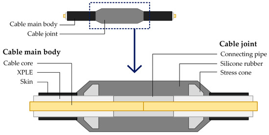
Figure 1.
Schematic of a 10 kV cross-linked polyethylene (XLPE) cable and the joint.
2.2. Charge Simulation Based Electric Field Calculation
Electric field distributions around the cable joint were calculated based on the CSM. The CSM simulates the field by a number of discrete charges placed outside the calculation region to solve Poisson’s equations with boundary conditions satisfied numerically [35].
The ring charges, line charges, and point charges were input in the XLPE main insulation, cable core, and defects, respectively, to fit the axis-symmetrical geometry of the joint. The discretized equations are formulated as follows to calculate the values of charges according to the Dirichlet and Neumann boundary conditions [22].
P is the m × n coefficient matrix, Q is the n × 1 unknown simulating charge matrix, and V is the m × 1 electric potential matrix at the contour points.
The charge distributions were shown in the following sections to satisfy the potential continuity (Dirichlet) and normal flux density continuity (Neumann) on the interfaces between different materials. The model was built on the MATLAB platform.
2.2.1. Charges Distribution Close to the Cable Joint and Its Accessories
The distribution of all simulation charges close to the cable joint and its accessories is shown in Figure 2.
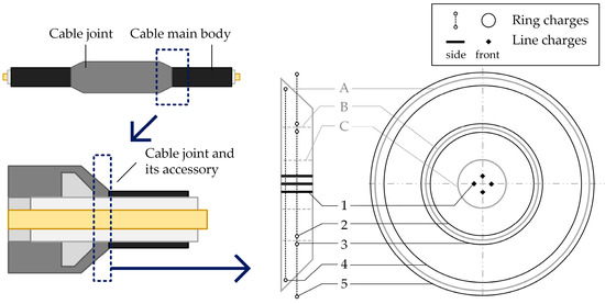
Figure 2.
Distribution of simulation charges close to the junction of the cable and the joint. Simulation charges: 1, Qcore, line charges in the cable core; 2, QXLPE.O, ring charges at the outer side of the XLPE layer; 3, QSiR.I, ring charges at the inner side of the silicone rubber; 4, QSiR.O, ring charges at the outer side of the silicone rubber; and 5, QA, ring charges close to the surface of the silicone rubber. Boundaries: A, the surface of the silicone rubber; B, the interface of silicone rubber and XLPE layer; and C, the interface of the XLPE layer and cable core.
The potential of the interface of cable core and XLPE layer is calculated as
where ncore is the number of line charges Qcore in the cable core, nSiR.I is the number of ring charges QSiR.I at the inner side of the silicone rubber, P is the potential coefficient, and φcore is the potential of the cable core.
The potential continuity boundary condition on the interface of the XLPE layer and silicone rubber, and the surface of the silicone rubber are calculated by Equations (4) and (5), respectively:
where nXLPE.O is the number of line charges QXLPE.O at the inner side of the XLPE layer, nSiR.O is the number of ring charges QSiR.O at the outer side of the silicone rubber, and nA is the number of ring charges QA close to the surface of the silicone rubber.
The field strength boundary conditions on the interface of the XLPE layer and the silicone rubber, and the surface of the silicone rubber are calculated by Equations (6) and (7), respectively:
where εXLPE, εSiR, and εA are the permittivity of XLPE, silicone rubber, and air, respectively.
2.2.2. Charges Distribution Close to the Stress Cone
The distribution of all simulation charges close to the stress cone shown in Figure 3.
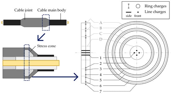
Figure 3.
Distribution of simulation charges close to the stress cone. Simulation charges: 1, Qcore, line charges in the cable core; 2, QXLPE.O, ring charges at the outer side of the XLPE layer; 3, QSC.I, ring charges at the inner side of the stress cone; 4, QSC.O, ring charges at the outer side of the stress cone; 5, QSiR.I, ring charges at the inner side of the silicone rubber; 6, QSiR.O, ring charges at the outer side of the silicone rubber; and 7, QA, ring charges close to the surface of the silicone rubber. Boundaries: A, the surface of the outer layer of the silicone rubber; B, the interface of the silicone rubber and the stress cone; C, the interface of the stress cone and the XLPE layer; and D, the interface of the XLPE layer and the cable core.
The potential of the interface of cable core and XLPE layer is calculated as:
where nSC.I is the number of ring charges QSC.I at the inner side of the stress cone.
The potential continuity boundary conditions on the interfaces of the XLPE layer–stress cone, stress cone–silicone rubber, and air–silicone rubber are satisfied by Equations (9)–(11) respectively:
where nSC.O is the number of ring charges QSC.O at the outer sides of the stress cone.
The field strength boundary conditions on the interfaces between XLPE layer–stress cone, stress cone–silicone rubber interfaces, and air-silicone rubber are satisfied by Equations (12)–(14), respectively:
where εSC is the permittivity of the stress cone material.
2.2.3. Charges Distribution Close to the Connecting Pipe Inside the Cable Joint
The distribution of all simulation charges close to the connecting pipe shown in Figure 4.
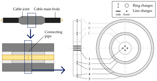
Figure 4.
Distribution of simulation charges inside the cable joint. Simulation charges: 1, Qcore, line charges in the cable core; 2, Qpipe.O, ring charges at the outer side of the connecting pipe; 3, QSiR.I, ring charges at the inner side of the silicone rubber; 4, QSiR.O, ring charges at the outer side of the silicone rubber; and 5, QA, ring charges close to the surface of the silicone rubber. Boundaries: A, the surface of the silicone rubber; B, the interface of silicone rubber and the connecting pipe; and C, the interface of connecting pipe and cable core.
The potential of the interface of the cable core and the connection pipe layer is calculated by:
The potential continuity boundary conditions on the interfaces between of the connecting pipe–silicone rubber and the silicone rubber-air are calculated by Equations (16) and (17), respectively:
where npipe.O is the number of ring charges Qpipe.O at the outer side of the connection pipe.
The field strength boundary conditions on the interface of connection pipe and silicone rubber are calculated by:
where εpipe is the permittivity of the connection pipe material.
2.2.4. Charges Distribution Close to Four Types of Defects
Four main kinds of defects occur on the interface of the XLPE layer and the silicone rubber: ware air voids, water film, metal debris, and metal needles shown in Figure 5.
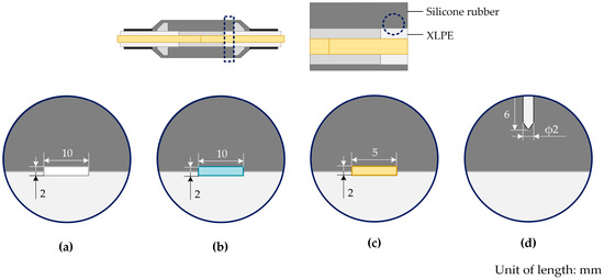
Figure 5.
Defects between the XLPE layer and the silicone rubber: (a) air void, (b) water film, (c) metal debris, and (d) metal needle.
For non-conductive defects, such as air voids or water films, a series of point charges are placed close to the interface of the defects and other materials (Figure 6), and the potential continuity and field strength boundary conditions must be satisfied.
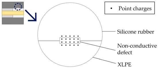
Figure 6.
Charges distribution of non-conductive defects.
The potential continuity equations are:
where nD.SiR and nD.XLPE are the numbers of the point charges QD.SiR and QD.XLPE at the rubber and XLPE sides inside the defect, respectively; and nSiR.D and nXLPE.D are the numbers of the point charges QSiR.D and QXLPE.D at the defect side inside the silicone rubber and XLPE layer, respectively.
The field boundary equations are:
where εD is the permittivity of the defect, such as the permittivity of air (εA) or water (εW).
Metal debris (Figure 7) has floating potential [36]. Hence, the calculation of metal debris is different from non-conductive defects.
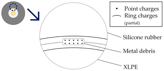
Figure 7.
Charges distribution of metal debris.
To calculate the potential of the metal debris, the potential boundary equations are:
where φM is the unknown potential of the metal debris and nM is the number of point charges QM inside the metal debris.
2.3. Electrical Tree Propagation Model
In this model, the trajectory of the electrical tree was composed of a sequence of point charges (Figure 8a).
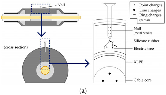
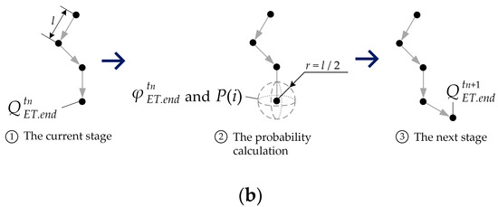
Figure 8.
Simulation model of the electrical tree: (a) charge distribution inside the metal needle and the electrical tree and (b) simulation of electrical tree development process.
Since the formation of the electrical tree is a time-varying process, the potential φ of each position inside the silicone rubber is calculated by:
where nMN and nET are the numbers of point charges QMN and QET inside the metal needle and on the electrical tree, respectively; and the superscript tn represents the nth state. The instant tn is related to the initial time t0 and the time step Δt, i.e.,
In this model, the length of the electrical tree propagation step is l. Thus, the probability of electrical tree development is related to the potential on a sphere with point charge based on random walk theory at the end of the electrical tree (Figure 8b). The calculation for potential is shown in Equation (26).
The number of possible development directions is ndir. For the i-th direction, its probability P(i) is calculated by [33,34]:
where is the potential on the sphere in the j-th direction and τ(φ) is a piecewise function:
where Edielectr is the dielectric strength of the silicone rubber. In other words, for electrical tree development the electric strength on the sphere must exceed the dielectric strength of the silicone rubber.
The program flow diagram is shown in Figure 9.
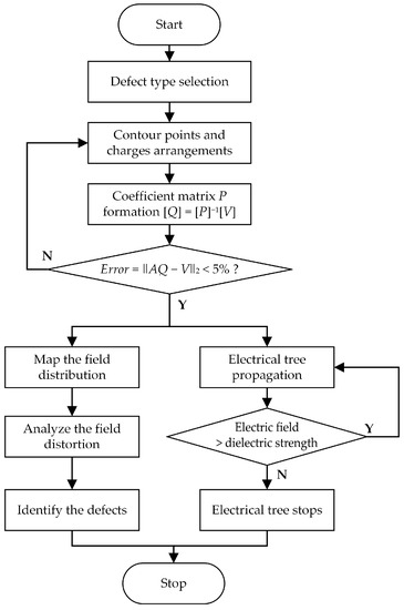
Figure 9.
The program flow chart for the simulation process.
3. Results
3.1. Simulation Results with Four Types of Defects
3.1.1. Electric Field Distribution with the Air Void Defect
Electric field distributions with the air void defect are shown in Figure 10. Figure 10a,b shows the location of the defect in the cylindrical cable joint structure. Figure 10c displays the electric field distribution in the front view of the cable joint. Figure 10d shows the electric field distribution with an air void defect along the measurement line in Figure 8a. Figure 10e presents the electric field strength on the cable joint surface along the measurement lines in Figure 10a,b.
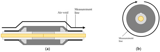
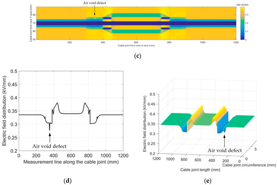
Figure 10.
Electric field distributions with the air void defect: (a) front view of defect and field measurement line in the cable joint, (b) cross-section view of defect and field measurement line of the cable joint, (c) front view of electric field distribution of the cable joint, (d) front view of electric field distribution along measurement line, and (e) electric field strength on the cable joint surface.
Figure 10c shows that the electric field strength increased in the air void defect area due to the small relative permittivity of air, and the electric field around the defect decreased (Figure 10d). Figure 10e illustrates that the electric field strength on the cable joint surface was distorted and evidently decreased in the area close to the air void defect.
3.1.2. Electric Field Distribution with the Water Film Defect
Electric field distributions with the water film defect are shown in Figure 11. Figure 11a,b shows the location of the defect in the cylindrical cable joint structure. Figure 11c displays the electric field distribution from the front view of the cable joint. Figure 11d shows the electric field distribution with the water film defect along the measurement line shown in Figure 11a. Figure 11e presents the electric field strength on the cable joint surface along the measurement lines from Figure 11a,b.
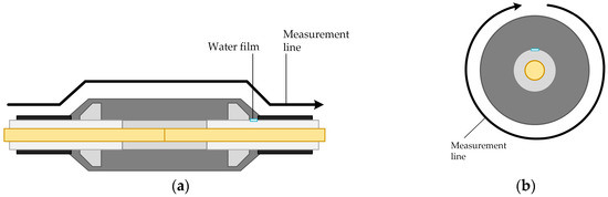
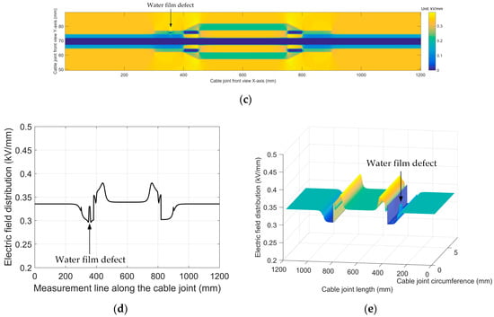
Figure 11.
Electric field distributions with the water film defect: (a) defect and field measurement line from the front view of the cable joint, (b) cross-section view of defect and field measurement line of the cable joint, (c) electric field distribution from the front view of the cable joint, (d) electric field distribution along the front view measurement line, and (e) electric field strength on the cable joint surface.
Figure 11c shows that the electric field strength decreased in the water film defect area due to the large relative permittivity of water, and the electric field around the defect increased (Figure 11d). Figure 11e illustrates that the electric field strength on the cable joint surface was distorted and evidently increased in the area close to the water film defect.
3.1.3. Electric Field Distribution with the Metal Debris Defect
Electric field distributions with the metal debris defect are shown in Figure 12. Figure 12a,b shows the location of the defect in the cylindrical cable joint structure. Figure 12c displays the electric field distribution from the front view of the cable joint. Figure 12d shows the electric field distribution with a metal debris defect along the measurement line from Figure 12a. Figure 12e presents the electric field strength on the cable joint surface along the measurement lines from Figure 12a,b.
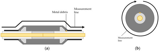
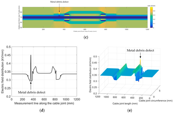
Figure 12.
Electric field distributions with the metal debris defect: (a) defect and field measurement line from the front view of the cable joint, (b) defect and field measurement line of the cross-section of the cable joint, (c) electric field distribution from the front view of the cable joint, (d) electric field distribution along the front view measurement line, and (e) electric field strength on the cable joint surface.
Figure 12c shows that the electric field strength decreased in the metal debris defect area due to the conductive property of the metal debris, and the electric field around the defect increased (Figure 12d). Figure 12e illustrates that the electric field strength on the cable joint surface was distorted and evidently increased in the area close to the metal debris defect.
3.1.4. Electric Field Distribution with the Metal Needle Defect
Electric field distributions with the metal needle defect are shown in Figure 13. Figure 13a,b shows the location of the defect in the cylindrical cable joint structure. Figure 13c displays the front view of the electric field distribution of the cable joint. Figure 13d shows the electric field distribution with the metal needle defect along the measurement line from Figure 13a. Figure 13e presents the electric field strength on the cable joint surface along the measurement lines from Figure 13a,b.
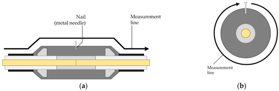
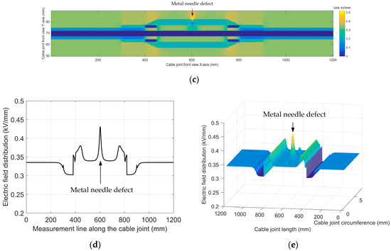
Figure 13.
Electric field distributions with the metal needle defect: (a) front view of the defect and field measurement line of the cable joint, (b) cross-section view of the defect and field measurement line of the cable joint, (c) electric field distribution from the front view of the cable joint, (d) electric field distribution along the front view measurement line, and (e) electric field strength on the cable joint surface.
Figure 13c shows that the electric field strength decreased in the metal needle defect area due to the conductive property of the metal needle, and the electric field around the defect increased (Figure 13d). Figure 13e shows that the electric field strength on the cable joint surface was distorted and evidently increased in the area close to the metal needle defect.
3.1.5. Electric Field Comparison with Four Types of Defects
The pattern of electric field distributions with four types of defects were analyzed based on the field distortion magnitude and tendency along the measurement lines on the cable joint surface. The characteristics of the field distributions for all types of defects are shown in Table 1.

Table 1.
Comparison of electric field distributions of four types of defects.
Table 1 shows that the field distortions of metal debris and needle were more severe than the field distortions caused by an air void and water film. The field distortion tendencies of air voids and water films were opposite. The types and locations of defects in the cable joint could be identified and located based on the characteristics of the measured electric field.
3.2. Experiment Results of Four Types of Defects
Electric field distribution along the measurement lines on the cable joint surface was measured using a probe based on the Pockels effect to reduce electromagnetic interference. The probe was installed on the ball screw structure to maintain a 10 mm distance from the top of the probe to the cable joint surface. The experiment schematic and setup are shown in Figure 14 and Figure 15, respectively. The supply voltage of the cable core was set to 7 kV AC (Line to ground).
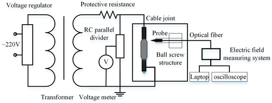
Figure 14.
Electric field measurement system schematic.
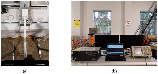
Figure 15.
Electric field measurement system setup: (a) the probe on the ball screw structure and (b) the electric field measurement equipment.
3.2.1. Artificial Defects in the Cable Joint
For the experiment, four typical defects were created to imitate the defects caused by external forces during cable joint manufacturing and installation processes (Figure 16).
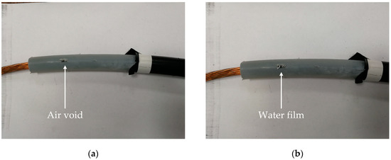
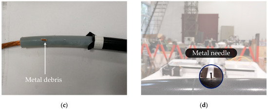
Figure 16.
Artificial defects in the cable joint: (a) air void, (b) water film, (c) metal debris, and (d) metal needle.
3.2.2. Electric Field Measurement Results
The electric field distribution was measured at discrete points around the cable joint surface. The location of the probe was accurately controlled by the ball screw structure to ensure that the distance between all the measurement points was 10 mm. The consecutive points were interpolated in the discrete measurement points to obtain the continuous plots in Figure 17 for four types of defects. The sizes and locations of the artificial defects were the same as the sizes and locations of the defects in the simulation model to enable comparison of the results. The electric field measurements were repeated five times at the same location close to the defect for each type of defect. The number of discrete points with more than 30% variance was less than 4% during the measurement. The maximum variances of the electric field strength from five repetitions are shown in Table 2.
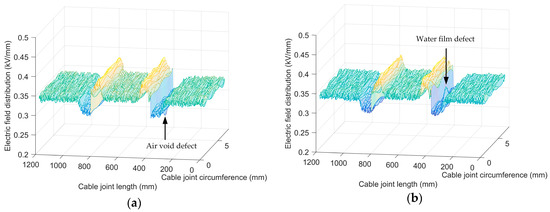
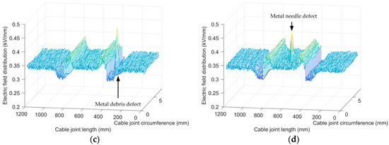
Figure 17.
Electric field measurement results around the cable joint surface with (a) the air void defect, (b) the water film defect, (c) the metal debris defect, and (d) the metal needle defect.
Table 2.
The maximum variances of the electric field strength from five repetitions.
It was observed that the variances of the repetitions were relatively small, and the number of repetitions did not significantly affect the accuracy of the measurement.
Figure 17 illustrates that electromagnetic interference and noise in the environment affects the accuracy of the electric field measurement. The accumulated errors between the simulation model and experiment results are shown in Table 3. From the experiment, it was concluded that the air void and water film defects could not be detected when their sizes were less than 5 mm3 because the field distortions caused by the air void and water film were relatively small and could be confused with the interference. The conductive metal defects could be identified and located when their sizes were larger than 2 mm3 due to the severe electric field distortion they produced.
Table 3.
Accumulated errors between the simulation and experiment results.
3.3. Simulation Results of Electrical Tree Propagation
The electrical tree propagation processes were simulated close to the defects, using the same types, locations, and sizes as in the electric field calculation model. The electrical tree initiated at the location with the maximum electric field strength and propagated for 9.2 min. The propagation processes were repeated 50 times to analyze the patterns of the tree trajectories.
Figure 18a shows that the average length of the electrical tree trajectories around the air void defects was 2.2 mm. The average length of the trajectories was small because the electric field around the air void defect decreased (Table 1) and the field distortion was mild. Figure 18b shows that the average length of the electrical tree trajectories around the water film defects was 4.7 mm. The average length of the trajectory increased because the electric field increased around the water film defect (Table 1). Figure 18c,d indicate that the average lengths of the electrical tree trajectories around the metal debris and needle defects were 7.5 mm and 11.2 mm, respectively, due to the severe electric field distortion around the defects. The electrical tree trajectories around the conductive metal defects tended to approach the cable core because the vertical field vector to the cable core was significantly larger than the field vectors in other directions during the tree propagation process.
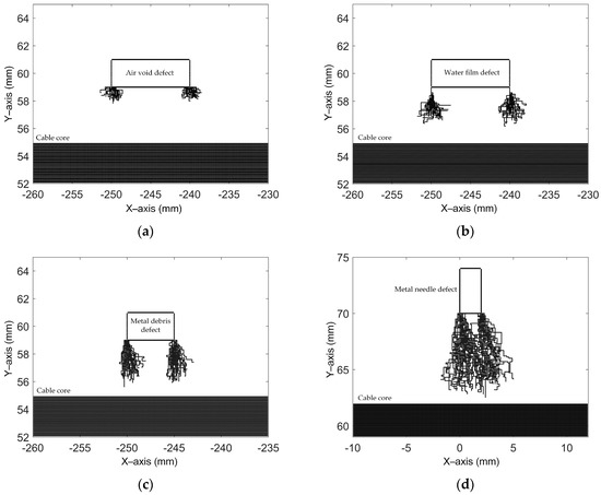
Figure 18.
Electrical tree distribution after propagation with (a) the air void defect, (b) the water film defect, (c) the metal debris defect, and (d) the metal needle defect.
4. Conclusions
The number of cable failure accidents continuously increased due to the defects produced during the manufacturing and aging processes, this paper provided a defect detection method for a 10 kV XLPE cable and predicted the aging rate based on the characteristics of the electric field distribution. The electric field distribution was calculated and measured around the defective cable surface. The simulation and calculation results were compared to validate the charge-simulation-based electric field model and the electric field measurements. The electrical tree propagation processes were simulated based on CSM and random walk theory to analyze the pattern of electrical tree trajectories.
- Four typical defects could be identified in the cable joint based on their unique electric field distribution characteristics. Electric field intensification was the original cause of insulation material breakdown, and the electric field measurement with Pockels effect reduced environmental interferences. A feature library of defects could be built for the operating personnel to locate and identify the internal and external defects.
- The electric field distortion magnitudes were 9.3%, 11.8%, 26.2%, and 29.7% for the defects of air void, water film, metal debris, and metal needle, respectively. The air and water defects of large size caused less field distortion when compared with metal defects of small size. Therefore, air void and water film defects were difficult to detect when they were smaller than 5 mm3 because their field distortions were relatively small and might be concealed by interference.
- The combination of CSM and random walk theory could accurately describe the electrical tree propagation in cable joints. CSM was used to calculate the instantaneous electric field and charge distributions at each step of tree propagation. Random walk theory describes the stochastic property of electrical tree growth by determining the tree propagation direction based on the electric field analysis and the probabilistic model. The electrical tree model could predict the aging rate of the insulation material and prevent the failure accident of the cable joint.
- The average length of the electrical tree trajectories around a water film defect was larger than those around an air void defect due to the opposite field distortion tendencies around the defect. The electrical trees around metal debris and needles were more inclined to approach the cable core and cause main insulation breakdown compared with other types of defects.
Author Contributions
Conceptualization: J.H.; Methodology: J.H.; Software: J.H. and K.H.; Validation: K.H. and L.C.; Formal Analysis: J.H. and K.H.; Investigation: J.H.; Experiment: L.C.; Writing—Original Draft Preparation: J.H.; Writing—Review and Editing: J.H., K.H., and L.C.
Funding
This research was supported by the National Natural Science Foundation of China (Grant No. 51807028), the Basic Research Program of Jiangsu Province (Grant No. BK20170672).
Conflicts of Interest
The authors declare no conflict of interest.
Nomenclature
| Edielectr | Dielectric strength of silicone rubber (unit: kV/mm) |
| l | Length step of electrical tree development (unit: mm) |
| nA | Number of ring charges in the air close to the silicone rubber |
| ncore | Number of line charges in the cable core |
| nD.SiR | Number of point charges in the defects close to the silicone rubber interface |
| nD.XLPE | Number of point charges in the defects close to the XLPE layer |
| ndir | Number of possible directions of electrical tree development |
| nET | Number of point charges in the electrical tree |
| nM | Number of point charges in the metal debris |
| nMN | Number of point charges in the metal needle |
| npipe.O | Number of ring charges at the outer side of the connecting pipe |
| nSC.I | Number of ring charges at the inner side of the stress cone |
| nSC.O | Number of ring charges at the outer side of the stress cone |
| nSiR.D | Number of point charges in the silicone rubber close to the defect interface |
| nSiR.I | Number of ring charges at the inner side of the silicone rubber |
| nSiR.O | Number of ring charges at the outer side of the silicone rubber |
| nXLPE.D | Number of point charges in the XLPE layer close to the defect interface |
| nXLPE.O | Number of ring charges at the outer side of the XLPE layer |
| P(i) | Probability of the i-th possible direction of electrical tree development |
| Pi,j | Potential coefficient (unit: kV/pC) |
| QA | Ring charges in the air close to the silicone rubber (unit: pC) |
| Qcore | Line charges in the cable core (unit: pC) |
| QD.SiR | Point charges in the defects close to the silicone rubber interface (unit: pC) |
| QD.XLPE | Point charges in the defects close to the XLPE layer (unit: pC) |
| QET | Point charges in the electrical tree (unit: pC) |
| Point charge at the end of the electrical tree at n-th stage (current stage, unit: pC) | |
| Point charge at the end of the electrical tree at (n + 1)-th stage (next stage, unit: pC) | |
| QM | Point charges in the metal debris (unit: pC) |
| QMN | Point charges in the metal needle (unit: pC) |
| Qpipe.O | Ring charges at the outer side of the connecting pipe (unit: pC) |
| QSC.I | Ring charges at the inner side of the stress cone (unit: pC) |
| QSC.O | Ring charges at the outer side of the stress cone (unit: pC) |
| QSiR.D | Point charges in the silicone rubber close to the defect interface (unit: pC) |
| QSiR.I | Ring charges at the inner side of the silicone rubber (unit: pC) |
| QSiR.O | Ring charges at the outer side of the silicone rubber (unit: pC) |
| QXLPE.D | Point charges in the XLPE layer close to the defect interface (unit: pC) |
| QXLPE.O | Ring charges at the outer side of the XLPE layer (unit: pC) |
| r | Radius of the sphere centered on , r = l/2 (unit: mm) |
| Δt | Time step of electrical tree development (unit: s) |
| t0 | Initial state of electrical tree development (unit: s) |
| tn | The n-th state (current state) of electrical tree development (unit: s) |
| tn + 1 | The (n + 1)-th state (next state) of electrical tree development (unit: s) |
| εA | Permittivity of air (unit: pF/m) |
| εD | Permittivity of dielectric of non-conductive defect (unit: pF/m) |
| εSC | Permittivity of material of stress cone (unit: pF/m) |
| εpipe | Permittivity of material of connecting pipe (unit: pF/m) |
| εSiR | Permittivity of silicone rubber (unit: pF/m) |
| εW | Permittivity of water (unit: pF/m) |
| εXLPE | Permittivity of XLPE (unit: pF/m) |
| φcore | Potential of cable core (unit: kV) |
| Potential of the sphere surface with as the center and l/2 as the radius(unit: kV) | |
| φM | Potential of metal debris (unit: kV) |
References
- Blodgett, R.B.; Fisher, R.G. Insulations and Jackets for Cross-Linked Polyethylene Cables. IEEE Trans. Power App. Syst. 1963, 82, 971–980. [Google Scholar] [CrossRef]
- McKean, A.L.; Oliver, F.S.; Trill, S.W. Cross-Linked Polyethylene for Higher Voltages. IEEE Trans. Power App. Syst. 1967, PAS-86, 1–10. [Google Scholar] [CrossRef]
- Pack, A.V. Service Aged Medium Voltage Cables – A Critical Review of Polyethylene Insulated Cables. In Proceedings of the Conference Record of the 2004 IEEE International Symposium on Electrical Insulation, Indianapolis, IN, USA, 19–22 September 2004. [Google Scholar]
- Zhang, C.; Li, C.; Zhao, H.; Han, B.A. Review on the Aging Performance of Direct Current Cross-linked Polyethylene Insulation Materials. In Proceedings of the 2015 IEEE 11th International Conference on the Properties and Applications of Dielectric Materials (ICPADM), Sydney, NSW, Australia, 19–22 July 2015. [Google Scholar]
- Thue, W.A. Electrical Power Cable Engineering, 3rd ed.; CRC Press: Boca Raton, FL, USA, 2011. [Google Scholar]
- Luo, H.; Cheng, P.; Liu, H.; Kang, K.; Yang, F.; Yang, Q. Investigation of Contact Resistance Influence on Power Cable Joint Temperature based on 3-D Coupling Model. In Proceedings of the 2016 IEEE 11th Conference on Industrial Electronics and Applications (ICIEA), Hefei, China, 5–7 June 2016. [Google Scholar]
- Ruan, J.; Liu, C.; Tang, K.; Huang, D.; Zheng, Z.; Liao, C. A Novel Approach to Estimate Temperature of Conductor in Cable Joint. In Proceedings of the 2015 IEEE International Magnetics Conference (INTERMAG), Beijing, China, 11–15 May 2015. [Google Scholar]
- Colavitto, A.; Contin, A.; Vicenzutti, A.; Sulligoi, G.; McCandless, M. Impact of Harmonic Pollution in Junctions between DC Cables with Different Insulating Technologies: Electrical and Thermal Analyses. In Proceedings of the 2019 IEEE Milan PowerTech, Milan, Italy, 23–27 June 2019. [Google Scholar]
- Kubota, T.; Takahashi, Y.; Hasegawa, T.; Noda, H.; Yamaguchi, M.; Tan, M. Development of 500-kV XLPE Cables and Accessories for Long Distance Underground Transmission Lines-Part II: Jointing Techniques. IEEE Trans. Power Deliv. 1994, 9, 1750–1759. [Google Scholar] [CrossRef]
- Takeda, N.; Lzumi, S.; Asari, K.; Nakatani, A.; Noda, H.; Yamaguchi, M.; Tan, M. Development of 500-kV XLPE Cables and Accessories for Long-distance Underground Transmission Lines. IV. Electrical Properties of 500-kV Extrusion Molded Joints. IEEE Trans. Power Deliv. 1996, 11, 635–643. [Google Scholar] [CrossRef]
- Yang, H.; Liu, L.; Sun, K.; Li, J. Impacts of Different Defects on Electrical Field Distribution in Cable Joint. J. Eng. 2019, 2019, 3184–3187. [Google Scholar] [CrossRef]
- Song, M.; Jia, Z. Calculation and Simulation of Mechanical Pressure of XLPE-SR Surface in Cable Joints. In Proceedings of the 2018 12th International Conference on the Properties and Applications of Dielectric Materials (ICPADM), Xi’an, China, 20–24 May 2018. [Google Scholar]
- Chen, C.; Liu, G.; Lu, G.; Wang, J. Influence of Cable Terminal Stress Cone Install Incorrectly. In Proceedings of the 2009 IEEE 9th International Conference on the Properties and Applications of Dielectric Materials, Harbin, China, 19–23 July 2009. [Google Scholar]
- Chen, C.; Liu, G.; Lu, G.; Wang, J. Mechanism on Breakdown Phenomenon of Cable Joint with Impurities. In Proceedings of the 2009 IEEE 9th International Conference on the Properties and Applications of Dielectric Materials, Harbin, China, 19–23 July 2009. [Google Scholar]
- Zhang, L.; LuoYang, X.; Le, Y.; Yang, F.; Gan, C.; Zhang, Y. A Thermal Probability Density-Based Method to Detect the Internal Defects of Power Cable Joints. Energies 2018, 11, 1674. [Google Scholar] [CrossRef]
- Yang, F.; Liu, K.; Cheng, P.; Wang, S.; Wang, X.; Gao, B.; Fang, Y.; Xia, R.; Ullah, I. The Coupling Fields Characteristics of Cable Joints and Application in the Evaluation of Crimping Process Defects. Energies 2016, 9, 932. [Google Scholar] [CrossRef]
- Yang, F.; Zhu, N.; Liu, G.; Ma, H.; Wei, X.; Hu, C.; Wang, Z.; Huang, J. A New Method for Determining the Connection Resistance of the Compression Connector in Cable Joint. Energies 2018, 11, 1667. [Google Scholar] [CrossRef]
- Zhu, W.; Zhao, Y.; Han, Z.; Wang, X.; Wang, Y.; Liu, G.; Xie, Y.; Zhu, N. Thermal Effect of Different Laying Modes on Cross-Linked Polyethylene (XLPE) Insulation and a New Estimation on Cable Ampacity. Energies 2019, 12, 2994. [Google Scholar] [CrossRef]
- Wang, Z.; Li, H.; Li, Y. PD Detection in XLPE Cable Joint based on Electromagnetic Coupling and Ultrasonic Method. In Proceedings of the 2011 International Conference on Electrical and Control Engineering, Yichang, China, 16–18 September 2011. [Google Scholar]
- Huang, Z.; Zeng, Y.; Wang, R.; Ma, J.; Nie, Z.; Jin, H. Study on Ultrasonic Detection System for Defects inside Silicone Rubber Insulation Material. In Proceedings of the 2018 International Conference on Power System Technology (POWERCON), Guangzhou, China, 6–8 November 2018. [Google Scholar]
- Jin, W.; Wang, H.; Kuffel, E. Application of the Modified Surface Charge Simulation Method for Solving Axial Symmetric Electrostatic Problems with Floating Electrodes. In Proceedings of the 1994 4th International Conference on Properties and Applications of Dielectric Materials (ICPADM), Brisbane, Queensland, Australia, 3–8 July 1994. [Google Scholar]
- Singer, H.; Steinbigler, H.; Weiss, P. A Charge Simulation Method for the Calculation of High Voltage Fields. IEEE Trans. Power Appl. Syst. 1974, PAS-93, 1660–1668. [Google Scholar] [CrossRef]
- Malik, N.H. A Review of the Charge Simulation Method and Its Applications. IEEE Trans. Electr. Insul. 1989, 24, 3–20. [Google Scholar] [CrossRef]
- Takuma, T.; Kawamoto, T.; Fujinami, H. Charge Simulation Method with Complex Fictitious Charges for Calculating Capacitive-Resistive Fields. IEEE Trans. Power App. Syst. 1981, PAS-100, 4665–4672. [Google Scholar] [CrossRef]
- Murooka, Y.; Nakano, T.; Takahashi, Y.; Kawakami, T. Modified Pockels Sensor for Electric-field Measurements. IEE Proc. Sci. Meas. Technol. 1994, 141, 481–485. [Google Scholar] [CrossRef]
- Long, F.; Zhang, J.; Xie, C.; Yuan, Z. Application of the Pockels Effect to High Voltage Measurement. In Proceedings of the 2007 8th International Conference on Electronic Measurement and Instruments, Xi’an, China, 16–18 August 2007. [Google Scholar]
- Talaat, M. Influence of Transverse Electric Fields on Electrical Tree Initiation in Solid Insulation. In Proceedings of the 2010 Annual Report Conference on Electrical Insulation and Dielectic Phenomena, West Lafayette, IN, USA, 17–20 October 2010. [Google Scholar]
- Song, W.; Zhang, D.; Wang, X.; Lei, Q. Characteristics of Electrical Tree and Effects of Barriers on Electrical Tree Propagation under AC Voltage in LDPE. In Proceedings of the 2009 IEEE 9th International Conference on the Properties and Applications of Dielectric Materials, Harbin, China, 19–23 July 2009. [Google Scholar]
- Wang, W.; Chen, S.; Yang, K.; He, D.; Yu, Y. The Relationship between Electric Tree Aging Degree and the Equivalent Time-frequency Characteristic of PD Pulses in High Voltage Cable. In Proceedings of the 2012 IEEE International Symposium on Electrical Insulation, San Juan, PR, USA, 10–13 June 2012. [Google Scholar]
- Fujiwara, O. An Analytical Approach to Model Indirect Effect Caused by Electrostatic Discharge. IEICE Trans. Commun. 1996, E79-B, 483–489. [Google Scholar]
- Champion, J.V.; Dodd, S.J. Modelling Partial Discharges in Electrical Trees. In ICSD’98. In Proceedings of the 1998 IEEE 6th International Conference on Conduction and Breakdown in Solid Dielectrics, Vasteras, Sweden, 22–25 June 1998. [Google Scholar]
- Zhou, Y.; Zhang, Y.; Zhang, L.; Guo, D.; Zhang, X.; Wang, M. Electrical tree Initiation of Silicone Rubber after Thermal Aging. IEEE Trans. Dielectr. Electr. Insul. 2016, 23, 748–756. [Google Scholar] [CrossRef]
- Noskov, M.D.; Malinovski, A.S.; Sack, M.; Schwab, A.J. Self-consistent Modeling of Electrical Tree Propagation and PD Activity. IEEE Trans. Dielectr. Electr. Insul. 2000, 7, 725–733. [Google Scholar]
- Noskov, M.D.; Malinovski, A.S.; Sack, M.; Schwab, A.J. Modelling of Partial Discharge Development in Electrical Tree Channels. IEEE Trans. Dielectr. Electr. Insul. 2003, 10, 425–434. [Google Scholar] [CrossRef]
- Zhou, P.B. Numerical Analysis of Electromagnetic Fields, 1st ed.; Springer Verlag: Berlin, Germany, 1993. [Google Scholar]
- El-Kishky, H.; Gorur, R.S. Electric Potential and Field Computation along AC HV Insulators. IEEE Trans. Dielectr. Electr. Insul. 1994, 1, 982–990. [Google Scholar] [CrossRef]
© 2019 by the authors. Licensee MDPI, Basel, Switzerland. This article is an open access article distributed under the terms and conditions of the Creative Commons Attribution (CC BY) license (http://creativecommons.org/licenses/by/4.0/).