Abstract
In this paper, two types of high step-up coupled inductor inverters based on qSBIs (quasi- switched boost inverters) are proposed. By applying the coupled inductor to the qSBIs, the voltage gain of the proposed inverter is regulated by turn ratio and duty ratio. Thus, a high voltage gain can be achieved without the circuits operating at the extreme duty cycle by choosing a suitable turn ratio of the coupled inductor. In addition, the proposed circuits have the characteristics of continuous input current and low voltage stress across the passive components. A boost unit can be added to the proposed inverters for further improvement of the voltage gain. In this paper, the working principle, steady state analysis, and the comparisons of the proposed inverter with other impedance-source inverters are described. A 200 W prototype was created and the experimental results confirm the correctness of the analysis in this paper.
1. Introduction
As the world’s energy structure has changed, renewable energy sources have been widely used in power generation, especially solar energy, such as photovoltaic (PV) power generation. Inverters with high voltage gain ability are used to connect new energy sources to the grid. This requires a PV generation system with high efficiency and high reliability. The Z-source inverter (ZSI) was first proposed in [1] to implement single-stage converter conversion with a buck-boost function. However, due to some shortcomings of the Z-source network, such as limiting boosting capability, discontinuous input current, no common ground, large starting current, and high voltage stress of the passive components, these features limit its wide application. Therefore, researchers have proposed many switching boost/quasi-switch boost inverters [1,2,3,4,5,6] instead of Z-source/quasi Z-source inverters (ZS/qZSIs). A switched boost inverter (SBI), which consists of one more active switch and a lower number of passive components than the ZSI, is proposed in [7]. In particular, its switch is only an auxiliary switch for which the voltage and current stress are low, unlike the switch of the cascade circuit. However, in the SBI, the voltage stress of the capacitor is equal to the DC link voltage. As the output voltage increases, the voltage stress across the capacitor becomes higher. Furthermore, the high voltage level capacitor increases the cost of the circuit. In addition, the input current is discontinuous in this circuit. Compared with the SBI, the quasi-SBI (qSBI) [2] has low voltage stress of the capacitor and continuous input current. Two embedded-type qSBIs are shown in Figure 1. The voltage gain is defined by:
D is the duty cycle in a period and denotes the peak DC-link voltage.
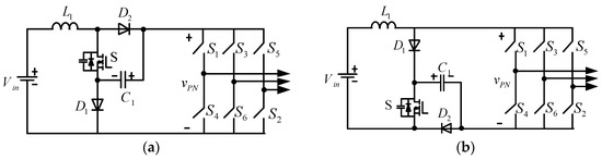
Figure 1.
(a) Type I qSBI and (b) type II qSBI (qSBIs: quasi-switched boost inverters).
To increase the boost ability of the qSBI, many improvements have been proposed in recent years. Many passive elements are applied to the qSBI. In [8] the diode-assisted/capacitor-assisted extended-boost, qZSI (DA/CA-qZSI) has been proposed; however, its voltage gain is not very high even though some passive elements are applied. A switched-inductor (SL) cell was added to the qSBI in [9,10] for a higher output voltage, but the voltage stress across the capacitor, diode, and switch is large, which is equal to the output voltage. A switched capacitor (SC) has been used in the qSBI [11], but the voltage gain does not achieve the desired effect and the voltage stress of the switch S0 is also high. Moreover, conventional boost converters generally cannot achieve very high voltage gains, and the duty cycle is extremely high due to parasitic parameters [12].
Determining how to properly apply components to obtain a high output voltage with low voltage stress across the switch and acheive a suitable non-extreme duty cycle has become a hot issue in research. In order to solve the above problems, this paper proposes a new type of qSBI inverter based on the coupled inductor. In the converters, with a reasonable design of the turn ratio of the coupled inductor, the high voltage gain can be achieved while avoiding extreme duty cycles [13,14,15,16,17,18]. Moreover, in the proposed circuit, the switch only plays a supporting role, so the voltage and current stresses of the switch can be low. Therefore, the proposed inverters have the features of high voltage gain and small voltage stress across the components. In addition, the converters have the advantage of a voltage gain that can also be increased by adjusting the turns ratio of the coupled inductor, so that a high boost ability can be obtained with a suitable duty cycle, and the voltage and current stress of the switch is low. It is also possible to extend the proposed inverter by adding cascade cells to increase voltage gain.
The organization of this paper is as follows. Firstly, the research background is introduced, and the idea of applying a coupled inductor to a qSBI circuit is proposed. The second chapter analyzes the principle of the circuit, including the converter’s operating mode, the voltage gain, device voltage and current stress, and the modulation scheme. The third chapter compares the proposed circuit with other similar circuits. The fourth chapter constructs an experimental platform and analyzes the experimental results. The final chapter is the conclusion, summarizing the full paper and demonstrating the effectiveness of the proposed circuit.
2. Proposed Inverter Topologies
The proposed converters are shown in Figure 2, where one capacitor (C2), one coupled inductor (N1, N2), and one diode (D3) are applied to the qSBIs. Type 1 circuit is shown in Figure 2a, and the ground node of its input voltage is directly connected to the negative node of the three-phase bridge circuit. The other is shown in Figure 2b, in which the ground node of the input voltage is not directly connected. The two circuits all consist of the coupled inductor (N1 and N2), an active switch (S), two capacitors (C1 and C2) and three diodes (D1, D2 and D3), with a three-phase bridge unit. In this paper, the type 1 topology of the proposed inverters is analyzed and verified as an example.
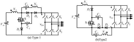
Figure 2.
The topology of the proposed inverters (a) Type 1; (b) Type 2.
2.1. Operation Modes
The equivalent circuit of the proposed type 1 converter is shown in Figure 3. In order to facilitate the circuit analysis of the proposed converter, some preconditions are shown as follows:
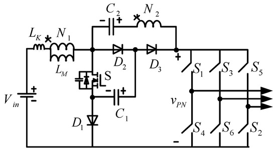
Figure 3.
Equivalent circuit of the proposed type 1 inverter.
- (1)
- The coupled inductor of the equivalent circuit can be composed of an ideal transformer with a turn ratio of n = N2:N1, a parallel magnetizing inductor LM, and a leakage inductance inductor LK.
- (2)
- The value of the capacitor is large enough to keep the capacitor voltage constant for one switching cycle.
- (3)
- The diodes are ideal, but the parasitic capacitance of the switch S cannot be ignored.
Based on the above assumptions, Figure 4 shows a partial waveform of the proposed converter in one switch cycle. The analysis of the four stages of operation is as follows.
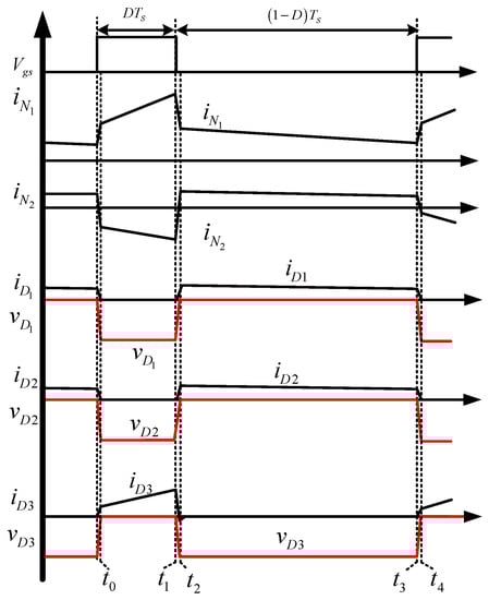
Figure 4.
Typical waveforms of the proposed converter during one switching period.
Stage I [t0, t1]: As shown in Figure 5a, the switch S turns on and the three-phase bridge unit operates in the shoot-through (ST) state. During this time period, diode D3 is turned on and diodes D1 and D2 are turned off. Input source Vin and the capacitor C1 are connected in series to charge the leakage inductance Lk and magnetizing inductance LM, thus the current IN1 increases linearly. At the same time, the energies of coupled inductor N2 and the capacitor C1 are released to the capacitor C2.
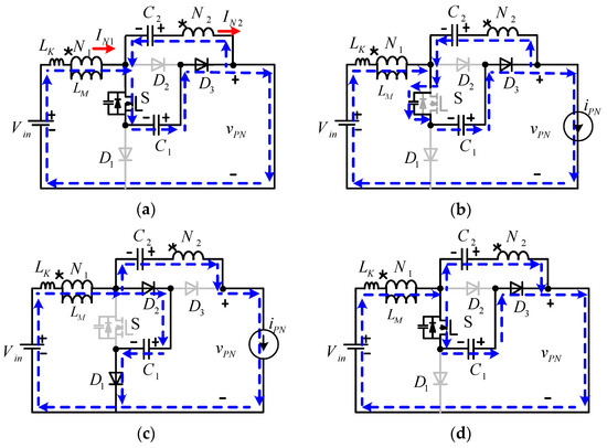
Figure 5.
Operating modes of the proposed inverter. (a) stage I; (b). stage II; (c). stage III; (d). stage IV.
Stage II [t1, t2]: In this time interval, the three-phase bridge unit operates in the non-through state (NST) and the switch S is turned off. Figure 5b shows the current-flow path. The diodes D1 and D2 are reverse-biased, and the diodes D3 forward-biased. The parasitic capacitor of the switch begins charging by winding of N1 and N2. The capacitor C2 is still working in the charging state. When the voltage of the parasitic capacitor of switch S is higher than the voltage of the capacitor C1 at t2, the diode D2 starts to conduct and this stage ends.
Stage III [t2, t3]: During this stage, the switch S is turned off and the three-phase bridge unit operates in the NST state. The diode D3 is reverse-biased and diodes D1 and D2 are forward-biased, as shown in Figure 5c. During this time interval, the capacitor C1 is charged by the input voltage Vin and the winding of N1. Meanwhile, the input source Vin, the capacitor C2, as well as the coupled inductor (N1 and N2), are in series to provide a high output voltage to the load.
Stage IV [t3, t4]: At t3, the switch S starts to turn on and the three-phase bridge unit operates in the shoot-through mode. During this transition interval, the current of N2 cannot be suddenly changed due to the presence of leakage inductance. As shown in the Figure 5d, the diodes D1 and D2 are reverse-biased because of the voltage of capacitor C1. In this stage, the winding of N1 is charged by the capacitor C1 and the input voltage Vin. When the current IN1 decreases to zero and begins to flow in the opposite direction, this stage ends, and the next switching period begins.
2.2. Math Derivations
In order to simplify the analysis of the proposed converter, the transient stage II and stage IV are neglected.
Applying the volt-second balance principle to the inductor, the following formula can be verified:
According to Equations (2)–(6), the voltages of capacitor C1 and capacitor C2 can be expressed as:
Thus, in stage III, the peak DC-link voltage VPN can be written as:
The boost factor can be defined as:
When the modulation index of the inverter is denoted as M, the duty cycle D will be limited to (1 − M), thus in this case, the peak voltage of the phase voltage in the AC side can be expressed as:
2.3. Voltage and Current Stress Analysis
For the sake of analysis, the capacitor voltage ripple has been ignored. From Figure 1a, the voltage stress of the diodes D1 and D2 can be expressed as:
During stage III, the voltage stress on the diode D3 and the switch S can be derived from:
The circuit on the AC side can be replaced by an equivalent resistance Rl on the DC side, when the three-phase bridge unit operates in a non-through state. Then, based on the calculation method in [2], the average DC link current IPN of the proposed inverter is:
Applying the principle of conservation of magnetic flux to the coupled inductor, the relationship between the inductor currents at different times can be expressed as:
Meanwhile, the relationship between and can be expressed by the following formula:
According to the charge and discharge balance of the capacitor C2, the values of and can be derived from:
According to Equations (17)–(20), the following equations can be obtained:
Therefore, the average current value of the diode D1, D2, D3 and S during the on-state period can be expressed as:
2.4. Modulation Scheme
The proposed inverter was modulated by the scheme of Space Vector Pulse Width Modulation (SVPWM). The synthesis voltage vector of the three-phase sinusoidal voltage is a rotating vector which can be called the reference voltage vector. Similar to the Z-source inverter, the proposed inverter has eight traditional non-through voltage vectors and one short-through zero voltage vector, as shown in Figure 6a. The non-through vectors are composed of six active vectors and two non-through zero voltage vectors, where the vertices of the six active voltage vectors form a regular hexagon. Note that the shoot-through vectors and non-through zero voltage vectors produce the same zero voltage to the load terminal. Therefore, the non-through zero vectors can be partially replaced with the short-through zero vector without affecting the load.
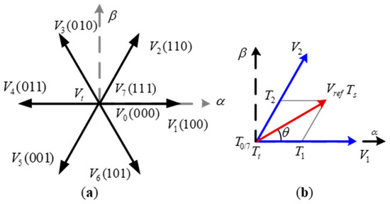
Figure 6.
(a) Space vector distribution; (b) vector synthesis.
As shown in the Figure 6a, the reference voltage vector at any location can be synthesized by two adjacent effective voltage vectors and zero voltage vectors. The effective time of the two adjacent effective voltage vectors required in one cycle can be obtained by the principle of vector synthesis. Taking the reference voltage vector in the first sector as an example, the synthesis of the reference vector has been shown in Figure 6b. Then, the following formula can be obtained:
where Ts represents a time period, T1 and T2, respectively, represent the time of the effective voltage vectors V1 and V2. T0/7 and Tt are the time of the NST zero vector (V0 or V7) and ST zero vector Vt. The value of T1, T2, T0 and Tt can be calculated as:
Compared with five-part SVPWM, the seven-part SVPWM can reduce the THD of output voltages and currents. The vectors sequence of the seven-part SVPWM scheme used in the proposed inverters is shown in Figure 7. The time of shoot-through zero vectors is divided into six segments and placed into voltage vector transition.
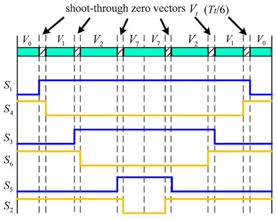
Figure 7.
The vectors sequence of seven-part SVPWM scheme. (SVPWM: Space Vector Pulse Width Modulation).
It can be seen that the seven-part SVPWM has an additional short-through state compared to the traditional SVPWM modulation; however, each phase leg still switches on and off once per switching cycle. The partial time of the non-through zero vectors is replaced by the short-through zero vectors, thus the active states time interval does not change. The short-through zero vectors increase the voltage of VPN, so at the same input voltage Vin and modulation M, the proposed inverter can output a higher AC voltage. According to the section of math derivations, the peak voltage of the phase voltage in the AC side was decided by D and M. That is to say, the desired output voltage can be realized by adjusting the short-through state time in SVPWM modulation while the voltage Vin has an obvious fluctuation, or not enough to directly generate a desired output voltage.
2.5. Extended Circuit
The proposed circuit can be extended for a higher output voltage. In this proposed extended circuit, two capacitors (C3 and C4) and two diodes (D4, D5), with the winding N3 are regarded as one cell. The voltage gain of the extended circuit will greatly increase as the number of cells increases. The extended circuit is shown in Figure 8.
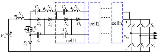
Figure 8.
Extended circuit of the proposed inverter.
3. Performance Comparisons
In order to better reflect the advantages of the proposed circuit, as shown in the Table 1, the proposed inverter has been compared with several other circuits, such as qSBI [2], ASC/SL-qZSI (Active-Switched-Capacitor/Switched-Inductor Quasi-Z-Source Inverters) [10], the converter in [19] and ASC/SCL-ZSI (Active-Switched-Capacitor/Switched-Capacitor-Inductor Z-Source Inverters) [20]. N2/N1 is represented by the parameter n in the comparison. Some important parameters in the circuit, such as the boost factor, switch stresses, maximum stresses of the diode and capacitor, and number of components are summarized in Table 1.

Table 1.
Comparison of the proposed converter with similar prototypes.
3.1. Number of Components
According to Table 1, compared with the qSBI [2], the proposed converter adds a coupled inductor and capacitor to obtain high voltage gain. The proposed converter has fewer components than the converters in [10,19,20]. Specifically, the proposed converter uses a smaller number of diodes, reducing the circuit cost and size.
3.2. Boost Factor
The biggest advantage of the proposed circuit is its voltage-boosting capability. It can be seen from Figure 9 that the boost factor of the proposed circuit is larger than those of the other three circuits with the same duty cycle. Although the voltage gain of the circuit in [20] is larger than the proposed circuit when the duty ratio D is greater than 0.175, the duty ratio of the converter in [20] reaches the limit at 0.2; therefore, the adjustment range is not as large as the proposed converter. Furthermore, the direct connection to the voltage source is an inductor rather than a diode, so the input current is continual, which benefits the power electronics applications, such as photovoltaic (PV) power generation systems.
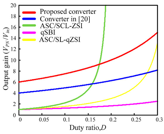
Figure 9.
Boost factor comparisons.
3.3. The Voltage Stresses of the Components
In order to better observe the comparison results of the voltage stress of each component, several graphs are drawn according to Table 1. For a fair comparison, the turns ratio of the coupled inductor is the same: n = 2. It can be seen from Figure 10 that the maximum voltage stress of the switch of the proposed circuit is the smallest, which is an attractive advantage. Because it reduces the switching loss, and some low-voltage switches can be applied to the circuit to reduce the circuit cost. According to Figure 11, it can be found that the maximum voltage stress of the capacitors in the proposed circuit is smaller than the converters in [2,10], and is nearly equal to the converter in [19,20].
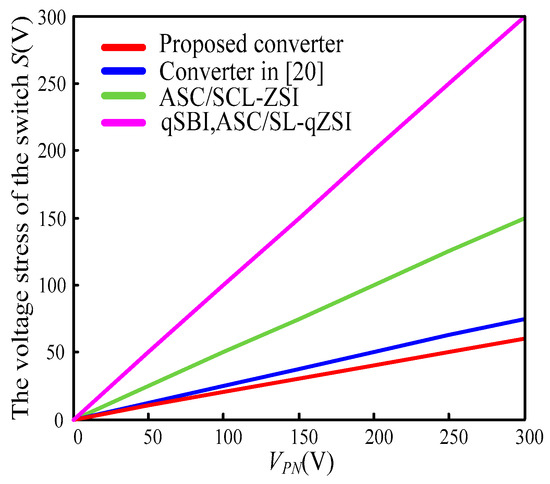
Figure 10.
The voltage stress of the switch comparisons.
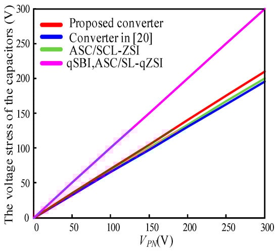
Figure 11.
The voltage stress of the capacitors comparisons.
4. Experimental Results
In order to verify the correction of the analysis of the proposed inverter, an experimental circuit of 200 W was built and tested. The prototype of the experimental setup is shown in Figure 12, which includes the main circuit topology, switch drive circuit, modulation circuit, and DSP (Digital Signal Processing) control board. The parameters of the experiment are shown in Table 2. The power of the experimental circuit was 200 W, with an input voltage of 24 V, a duty ratio equal to 0.2, and a turn ratio of 2, which can be applied in photovoltaic power generation.
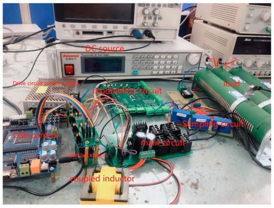
Figure 12.
The prototype of the experimental setup.
Table 2.
Parameters of the experiment.
The results of the experiment are shown in the Figure 13. The input voltage Vin and peak DC-link voltages VPN are shown in Figure 13a. Figure 13b shows the voltage of the capacitors C1 and C2. According to Figure 13c, the input current is continuous. It can be seen from Figure 13b,d that the voltage stresses of diode D1 and D2 are equal to the voltage of capacitor C1. Figure 13e shows the voltage waveform and current waveform of the switch S. The result of the experiment shows that the voltage stress of the switch is equal to capacitor C1 voltage, which is in line with the theoretical analysis results. The line voltage and phase current at the AC side of the converter are shown in Figure 13f. The efficiency of the proposed inverter under different loads is shown in Figure 14. The highest efficiency is 93.1% when the input voltage is 24 V and the output power is 250 W.
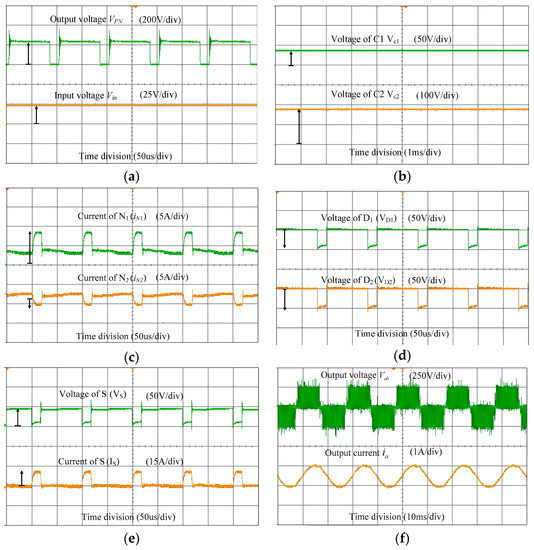
Figure 13.
Experimental waveforms for the proposed inverter: (a) The input voltage Vin and the peak DC-link voltages VPN; (b) The voltage of the capacitor C1 and C2; (c) The current of N1 and N2; (d) The voltage stresses of diode D1 and D2; (e) The voltage and current of the switch S; (f) The output voltage Vac and the output current ia.
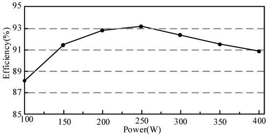
Figure 14.
Measured efficiency of the converter.
5. Conclusions
Two novel high step-up coupled inductor inverters based on qSBIs were proposed in this paper. Compared with the qSBI, these circuits use a coupled inductor and add one capacitor and one diode. The proposed circuits have the characteristics of high voltage gain and low voltage stress across the passive components. Due to the application of the coupled inductor, a high voltage gain can be achieved without the circuits operating at the extreme duty cycle. The voltage stress of the switch S is small, which is beneficial to reduce the losses, and improve the efficiency of the converter. In addition, a repeating boost unit can be added to the proposed inverters for further improvement of the voltage gain. Therefore, the proposed converter can be widely applied to the field of new energy power generation. The experimental results of input voltage 24 V and output voltage 240 V verify the performance of the proposed inverter and the experimental waveforms verify the theoretical analysis. In future work, attention should be paid to reducing the voltage spike on the main switch caused by the use of the coupled inductor; a problem that often occurs in converters that are based on the coupled inductor, and one that affects the efficiency of the converter. The passive clamp circuit can be applied to reduce the effect of leakage inductance, and the high-performance MOSFET can be used to improve the converter efficiency.
Author Contributions
Conceptualization, H.L. and X.S.; methodology, H.L.; software, J.W.; validation, X.S. and J.W.; formal analysis, H.L.; investigation, J.W.; resources, H.L.; data curation, X.S.; writing—original draft preparation, X.S.; writing—review and editing, H.L.; supervision, H.L.; project administration, H.L.; funding acquisition, H.L.
Funding
This research was funded by the National Natural Science Foundation of China (51777043), State Key Laboratory of Electrical Insulation and Power Equipment (EIPE18208), Natural Science Foundation of Heilongjiang Province of China (E2017035).
Conflicts of Interest
The authors declare no conflict of interest.
References
- Peng, F. Z-source inverter. IEEE Trans. Ind. Appl. 2003, 39, 504–510. [Google Scholar] [CrossRef]
- Nguyen, M.; Le, T.; Lim, Y. A Class of Quasi-Switched Boost Inverters. IEEE Trans. Ind. Electron. 2015, 62, 1526–1536. [Google Scholar] [CrossRef]
- Nguyen, M.; Lim, Y.; Kim, Y. TZ-Source Inverters. IEEE Trans. Ind. Electron. 2013, 60, 5686–5695. [Google Scholar] [CrossRef]
- Mo, W.; Loh, P.C.; Blaabjerg, F. Asymmetrical Γ-source inverters. IEEE Trans. Ind. Electron. 2014, 61, 637–647. [Google Scholar] [CrossRef]
- Ravindranath, A.; Mishra, S.K.; Joshi, A. Analysis and PWM control of switched boost inverter. IEEE Trans. Ind. Electron. 2013, 60, 5593–5602. [Google Scholar] [CrossRef]
- Nag, S.S.; Mishra, S. Current-Fed Switched Inverter. IEEE Tran. Ind. Electron. 2014, 61, 4680–4690. [Google Scholar] [CrossRef]
- Mishra, S.; Adda, R.; Joshi, A. Inverse Watkins–Johnson Topology-Based Inverter. IEEE Trans. Power Electron. 2012, 27, 1066–1070. [Google Scholar] [CrossRef]
- Gajanayake, C.J.; Luo, F.L.; Gooi, H.B.; So, P.L.; Siow, L.K. Extended-Boost Z-Source Inverters. IEEE Trans. Power Electron. 2010, 25, 2642–2652. [Google Scholar] [CrossRef]
- Nguyen, M.; Le, T.; Park, S.; Lim, Y.; Yoo, J. Class of high boost inverters based on switched-inductor structure. IET Power Electron. 2015, 8, 750–759. [Google Scholar] [CrossRef]
- Ho, A.; Chun, T.; Kim, H. Extended Boost Active-Switched-Capacitor/Switched-Inductor Quasi-Z-Source Inverters. IEEE Trans. Power Electron. 2015, 30, 5681–5690. [Google Scholar] [CrossRef]
- Nguyen, M.; Duong, T.; Lim, Y.; Kim, Y. Switched-Capacitor Quasi-Switched Boost Inverters. IEEE Trans. Ind. Electron. 2018, 65, 5105–5113. [Google Scholar] [CrossRef]
- Wai, R.J.; Lin, C.Y.; Duan, R.Y. High-efficiency dc–dc converter with high voltage gain and reduced switch stress. IEEE Trans. Ind. Electron. 2007, 54, 354–364. [Google Scholar] [CrossRef]
- Vazquez, N.; Estrada, L.; Hernandez, C.; Rodriguez, E. The Tapped-Inductor Boost Converter. In Proceedings of the IEEE International Symposium on Industrial Electronics, Vigo, Spain, 4–7 June 2007; pp. 538–543. [Google Scholar]
- Li, W.; Li, W.; Xiang, X.; Hu, Y.; He, X. High Step-Up Interleaved converter with built-in transformer voltage multiplier cells for sustainable energy applications. IEEE Trans. Power Electron. 2014, 29, 2829–2836. [Google Scholar] [CrossRef]
- Berkovich, Y.; Axelrod, B. Switched-coupled inductor cell for DC-DC converters with very large conversion ratio. IET Power Electron. 2011, 4, 309–315. [Google Scholar] [CrossRef]
- Ajami, A.; Ardi, H.; Farakhor, A. A Novel high step-up dc/dc converter based on integrating coupled inductor and switched-capacitor techniques for renewable energy applications. IEEE Trans. Power Electron. 2015, 30, 4255–4263. [Google Scholar] [CrossRef]
- Wu, T.; Lai, Y.; Hung, J.; Chen, Y. Boost converter with coupled inductors and buck–boost type of active clamp. IEEE Trans. Ind. Electron. 2008, 55, 154–162. [Google Scholar] [CrossRef]
- Liu, H.; Li, F.; Ai, J. A novel high step-up dual switches converter with coupled inductor and voltage multiplier cell for a renewable energy system. IEEE Trans. Power Electron. 2016, 31, 4974–4983. [Google Scholar] [CrossRef]
- Hu, X.; Gong, C.A. High voltage gain dc–dc converter integrating coupled-inductor and diode–capacitor techniques. IEEE Trans. Power Electron. 2014, 29, 789–800. [Google Scholar]
- Bajestan, M.M.; Shamsinejad, M.A. Two new magnetically coupled-inductor Z-source inverters with high voltage boost capability. In Proceedings of the 2018 9th Annual Power Electronics, Drives Systems and Technologies Conference (PEDSTC), Tehran, Iran, 13–15 February 2018; pp. 419–425. [Google Scholar]
© 2019 by the authors. Licensee MDPI, Basel, Switzerland. This article is an open access article distributed under the terms and conditions of the Creative Commons Attribution (CC BY) license (http://creativecommons.org/licenses/by/4.0/).