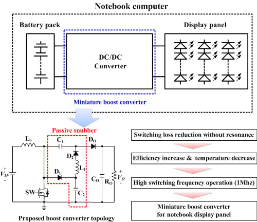
1. Introduction
Notebook or tablet computers are powered by a Li ion battery pack [
1,
2,
3,
4]. Typically, the battery pack is composed of 2–4 Li ion battery cells. Each Li ion cell has a terminal voltage of 2.6–4.2 V depending on the charging state, so the voltage of the battery pack changes in the range of 5–17 V [
5,
6,
7]. To supply power to each part of the computer, the pack voltage is converted to several voltages by DC-DC converters.
Many computers use a light-emitting diode (LED) backlight unit (BLU) for the liquid crystal display (LCD) panel. For a 17 inch panel, the voltage required to drive the LED backlight can be as high as 40 V [
8]. The DC-DC boost converter for the LED BLU in a notebook or tablet computer should have a circuit topology that can reduce the overall size and weight [
9,
10,
11,
12,
13,
14,
15,
16]. The conventional boost converter (
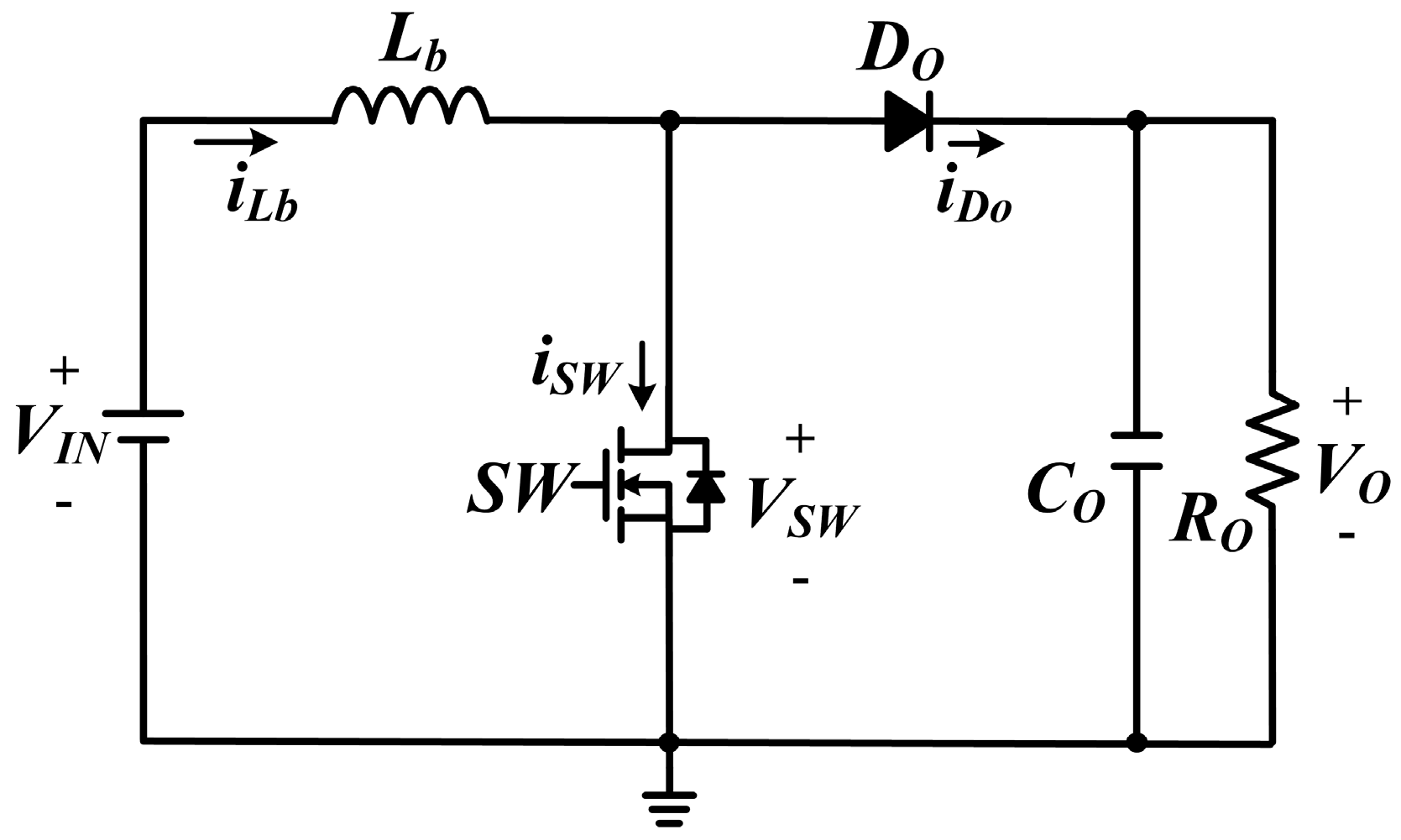
Figure 1) has the simplest structure, and can be implemented in small sizes by operating at a high switching frequency
fS. However, the switching loss increases as
fS increases, and thereby decreases the power conversion efficiency
ηe and can cause overheating of the switch. This problem has been solved using soft-switching converters [
17,
18,
19,
20,
21].
Soft-switching converters [
17,
18,
19,
20,
21] use active snubbers to reduce switching loss. These snubbers are implemented using an auxiliary switch, diodes, and energy storage elements. The auxiliary switch requires a separate gate drive circuit that is controlled by a sophisticated algorithm. The snubber of Reference [
17] discharges the drain-source capacitor
CDS of the main switch before the switch turns on, so zero-voltage (ZV) turn-on of the switch is possible. The snubbers of References [
18,
19] force the switch current to zero before the switch turns off, so zero-current (ZC) turn-off of the switch is possible. The snubber of Reference [
20] achieves ZV turn-off of the switch by reducing the rate of voltage increase during the turn-off transient, and achieves ZC turn-on of the switch by reducing the rate of current increase during the turn-on transient. However, the converters of References [
17,
18,
19,
20] have some limitations when they operate at high
fS; they use a resonance between an inductor (
L) and a capacitor (
C) in the active snubber, the inductance
L of L should be small enough to achieve ZV or ZC switching in a short time; the current peak of the switch or diodes increases as
L decreases, therefore, this change increases the conduction loss and reduces the maximum output power. In the converter of Reference [
21], the capacitance
CDS discharges through L of the snubber when the auxiliary switch turns on. The ZV turning on of the main switch is achieved by discharging
CDS completely. The
L required to achieve the ZV turning on of the switch decreases as
fS increases; as a consequence, the switching loss in the auxiliary switch increases. Therefore, simultaneous reduction of switching losses in the main and auxiliary switches is very difficult at high
fS. The converter of Reference [
9] uses a passive snubber to reduce the switching loss. The switching loss is reduced by lowering the turn-on slope of the switch current; the inductor
LS that is connected in series with the switch controls the turn-on slope. However, the energy stored in L
S is released as a voltage spike because the current path of
LS is blocked when the switch is turned off. To ensure that this voltage spike does not exceed the maximum voltage limit of the switch,
LS should be less than 50 nH at high switching frequencies; This value of
LS was calculated using Equation (9) of the design guide in Reference [
9]. The low value of the chip type inductor has a low maximum current limit. This low inductance also causes undesired resonance due to the parasitic inductance or capacitance of the circuit. Because of this, the converter of Reference [
9] is difficult to use at high switching frequencies. Additionally, the switch current significantly increases the conduction loss in
LS because the components of small size have non-negligible series resistance.
To improve upon the aforementioned drawbacks in the existing converters, this paper proposes a miniature DC-DC boost converter for the display panel of a notebook computer. The proposed converter (
Figure 2) uses a passive snubber to reduce the switching loss; the capacitor
C2 is connected in parallel with the switch, and the inductor
L1 is connected in series with
C2, and the value of
L1 and
C2 are large enough to prevent resonance at high
fS. This lowers
VSW to
VO-
VC1 and eliminates the switching loss. In addition,
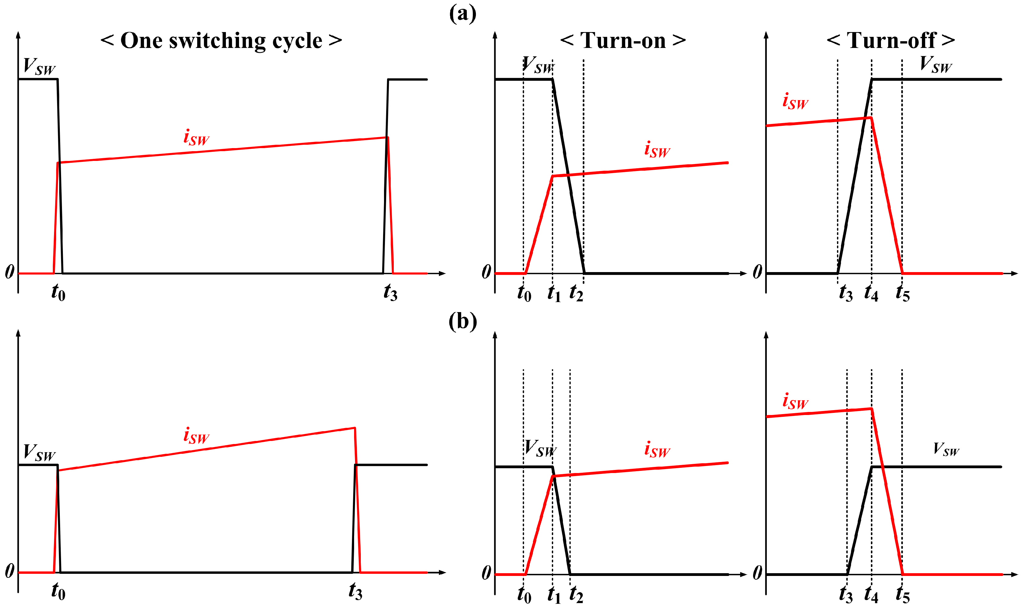
L1 is placed apart from the main current path to reduce the conduction loss in the passive snubber. The switch operates under a hard-switching condition to achieve fast switching, but the switching loss is reduced by lowering
VSW (
Figure 3). The switching loss
PSW is calculated using the waveforms of
iSW and
VSW as:
Compared with the conventional converter, the proposed converter has a similar current peak, but has VSW(t1) and VSW(t4) lowered by ~1/2, so PSW is reduced.
The proposed converter has a higher voltage conversion ratio than the conventional boost converter, and therefore has a wide range of output voltage for a given range of input voltage.
Section 2 describes the circuit structure and operating principle of the proposed converter,
Section 3 gives the design guidelines,
Section 4 shows the experimental results, and
Section 5 concludes the paper.
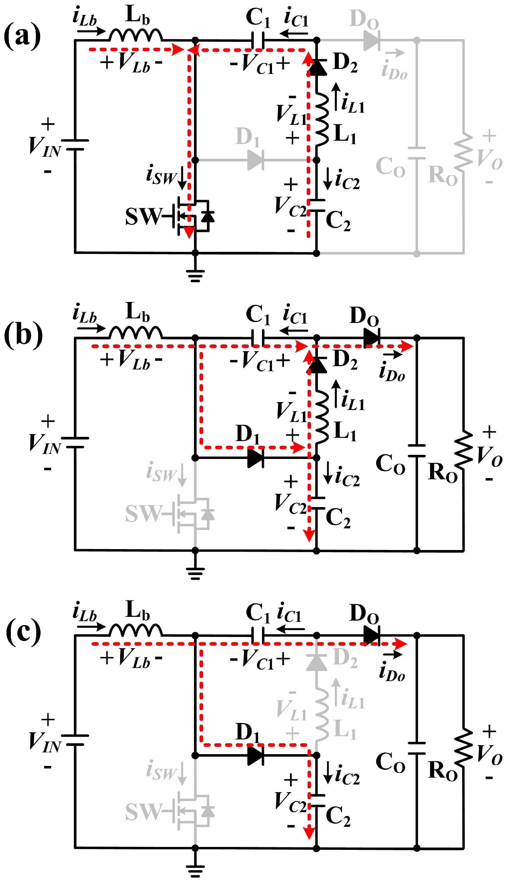
2. Circuit Structure and Operating Principles of the Proposed Converter
The proposed converter consists of two capacitors C1 and C2, two diodes D1 and D2, and an inductor L1, in addition to the conventional boost components Lb, DO, CO, and a switch (SW). C1 is located between boost inductor Lb and output diode DO, and acts as a charge pump capacitor to increase the voltage gain. L1 and C2 reduce the voltage stress of SW by dividing the output voltage VO. D1 and D2 provide a charging or discharging path for C2.
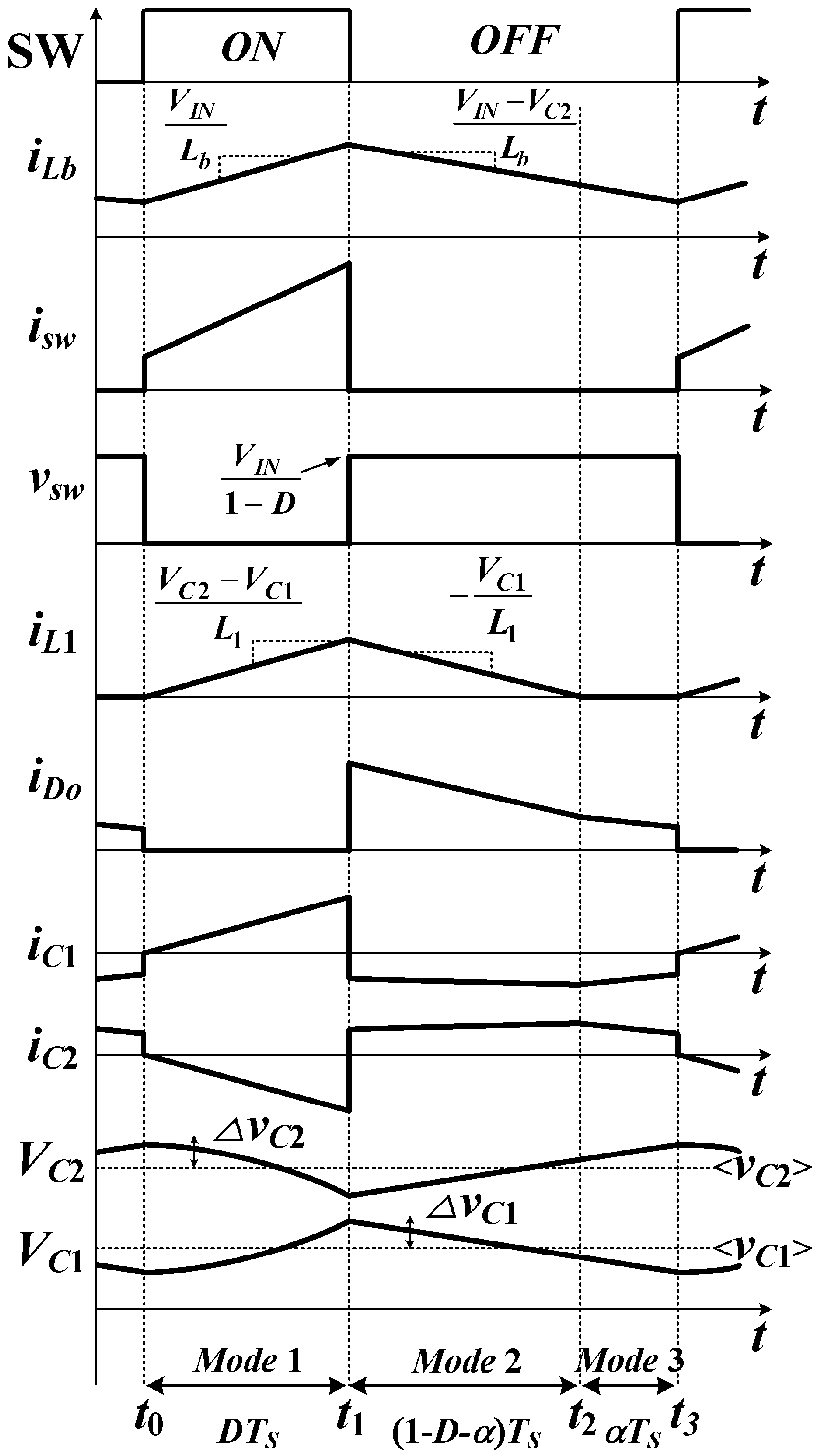
The operating modes (
Figure 4) and key waveforms (
Figure 5) of the proposed converter include three sequential modes of operation.
Mode 1 (
t0~
t1): The first operation (
Figure 4a) starts at
t =
t0 by turning ON SW. During this operation,
D2 turns ON, and
D1 and
DO turn OFF.
and
, so
C1 is charged and
C2 is discharged when SW is turned ON.
Mode 1 ends when SW is turned OFF.
Mode 2 (
t1~
t2): The second operation (
Figure 4b) starts at
t =
t1 when SW turns OFF. During
mode 2,
D2 stays ON, and
D1 and
DO are turned ON. When SW is turned OFF, the anode voltage of
D1 is
VC2 because
VLb =
VC2 −
VIN according to the voltage second valance law. The cathode voltage of
D1 is
VC2 − Δ
VC2 because C
2 was discharged in
Mode 1, so
D1 is turned ON. After
D1 is turned ON, the anode voltage of
DO is
VC1 +
VC2 and cathode voltage is
VO − Δ
VO because
CO was discharged in
Mode 1. Therefore,
DO is turned ON because
VC1 +
VC2 =
VO in steady state. In the same manner, after
D1 and
DO are turned ON,
D2 is turned ON because the anode voltage of
D2 is
VC1 +
VC2 and the cathode voltage is
VO − Δ
VO.
and
, so
The voltage stress of SW is VC2 because D1 is turned ON when SW is turned OFF. The output voltage VO is divided into VC1 and VC2, so the voltage stress of SW is smaller than VO, which is the voltage stress of the conventional boost converter.
Mode 3 (
t2~
t3): The last operation (
Figure 4c) starts at
t =
t2 when
D2 turns OFF.
D1 and
DO stay ON during this mode.
, so
In this mode, because iL1 = 0. Mode 3 ends when SW is turned ON for the next switching cycle.
The voltage–second balance law of inductances
Lb and
L1 yields
where
D is the duty of switching and
αTS is the duration of
Mode 3. Solving Equations (3) and (4) for
VC1 and
VC2 yields
Equation (5) and
then give the voltage conversion ratio as
The average current of
L1,
IL1 for one switching period
TS is equal to the average output current
IO, so
Inserting Equation (5) into Equation (7) and solving for
α yields
Combining Equations (6) and (8) yields the output voltage
VO versus
D (
Figure 6) for
L1 = 10 μH,
fS = 1 MHz,
IO = 150 mA,
VIN = 5 V, and 0.1 ≤
D ≤ 0.9 was calculated using Equation (9) for the proposed converter, but the conventional boost converter was calculated using their voltage gain equations. To have
VO = 40 V for given
VIN,
D = 0.775 was applied to the proposed converter, whereas
D = 0.875 was applied to the conventional boost converter. At given
VIN and
D, the proposed converter had higher
VO than the conventional boost converters.
4. Experimental Results
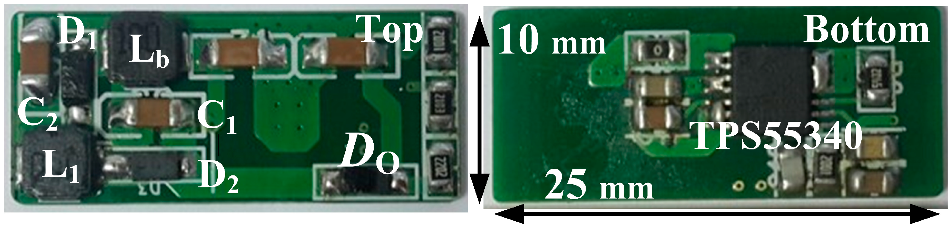
The proposed boost converter (
Figure 7) was designed to operate at
VIN = 5 V,
VO = 40 V, 30 ≤
IO ≤ 150 mA, and
fS = 1 MHz. The inductances were set at
Lb = 33 µH and
L1 = 10 µH. Capacitances
C1 and
C2 were both set at 1 µF. The experimental circuit was implemented using the following miniature components (
Table 1): TPS55340 DC-DC controller (Texas Instruments Inc., Dallas, TX, USA), which has an internal
n-MOS switch (40 V, 5A), RB160M-60TR diodes (Rohm Co.), IFSC-1515AH-01 (Vishay Inc.) and SSMC252008R47SC (SST Inc.) chip inductors, and multilayer ceramic chip capacitors of a size 3.2 mm × 1.6 mm. The chip inductors and capacitors have series resistances given in the parentheses. To ensure a fair comparison, the conventional boost converter used the same components.
The TPS55340 regulates the output voltage with current mode PWM control, and has an internal oscillator. The pulse width modulation of the gate pulse
Vg is achieved in the control circuit for the proposed converter (
Figure 8) as follows; each clock pulse resets the flip-flop and the ramp generator, which sets
Vg to the ‘high’ state; the output
Vc of the error amplifier increases as
VO increases; the comparator output changes from ‘low’ to ‘high’ when the output voltage of the ramp generator exceeds
Vc, which changes the inverter output
Vg to the ‘low’ state. When the output current
IO increases/decreases abruptly,
VO decreases/increases instantly, which increases/decreases
Vc. Thus, the pulse width of
Vg increases/decreases to keep
VO constant.
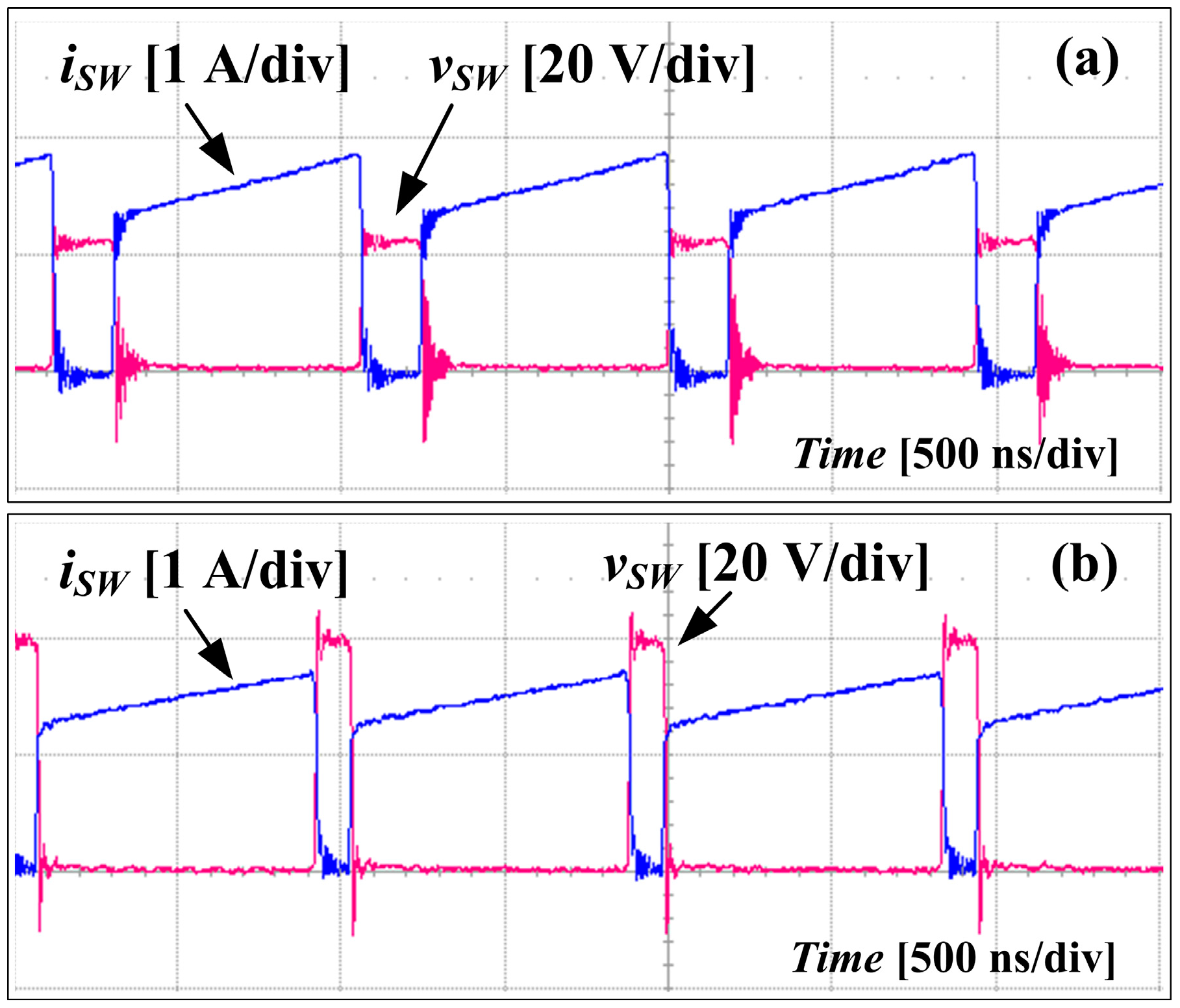
The voltage and current waveforms of SW (
Figure 9) were measured at
VIN = 5 V,
VO = 40 V,
IO = 150 mA, and
fS = 1 MHz. The voltage stress of the proposed converter (
Figure 9a) was lower than that of the conventional boost converter (
Figure 9b) because the voltage stress was
in the proposed converter but
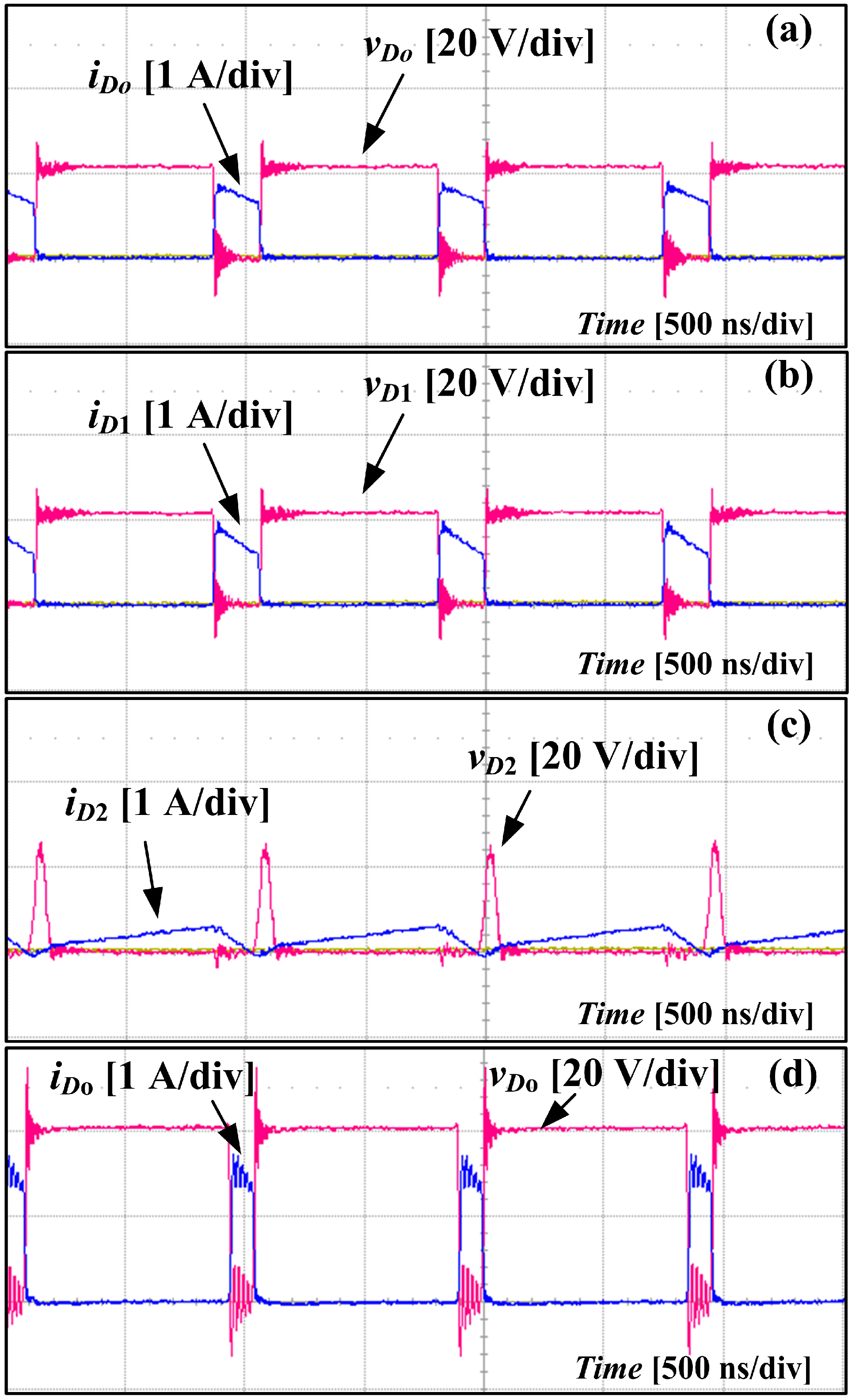
VO in the conventional boost converter. The current stresses of the proposed converter and the conventional boost converter were similar. The current waveforms of the diodes are shown in
Figure 10. The diodes current stresses of the proposed converter was lower than the conventional boost converter. The time-averaged values <
iD1>, <
iD2>, and <
iDo> were all equal to
IO.
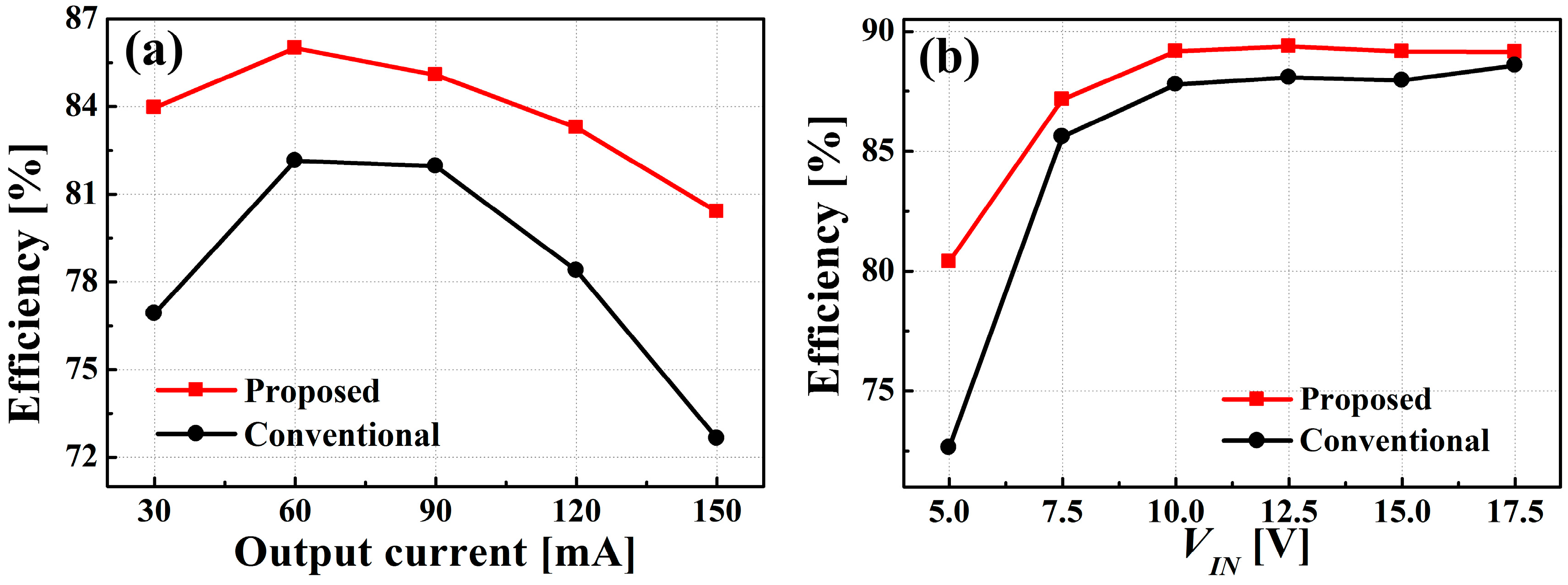
The curves of
ηe on
IO (
Figure 11a) were measured at 30 ≤
IO ≤ 150 mA,
VIN = 5 V,
VO = 40 V,
fS = 1 MHz. At
IO = 30 mA,
ηe was 84.0% for the proposed converter and 76.9% for the conventional boost converter. At
IO = 150 mA,
ηe was 80.4% for the proposed converter and 72.6% for the conventional boost converter. The curves of
ηe on
VIN (
Figure 11b) were measured at 5 ≤
VIN ≤ 17.5 V,
IO = 150 mA,
VO = 40 V,
fS = 1 MHz;
ηe at
VIN = 17.5 V was 89.1% for the proposed converter and 88.6% for the conventional boost converter. The
ηe of the proposed converter was up to 7.8% higher than the conventional boost converter at
VIN = 5 V. The proposed converter had a high
ηe over the entire input voltage and output current ranges.
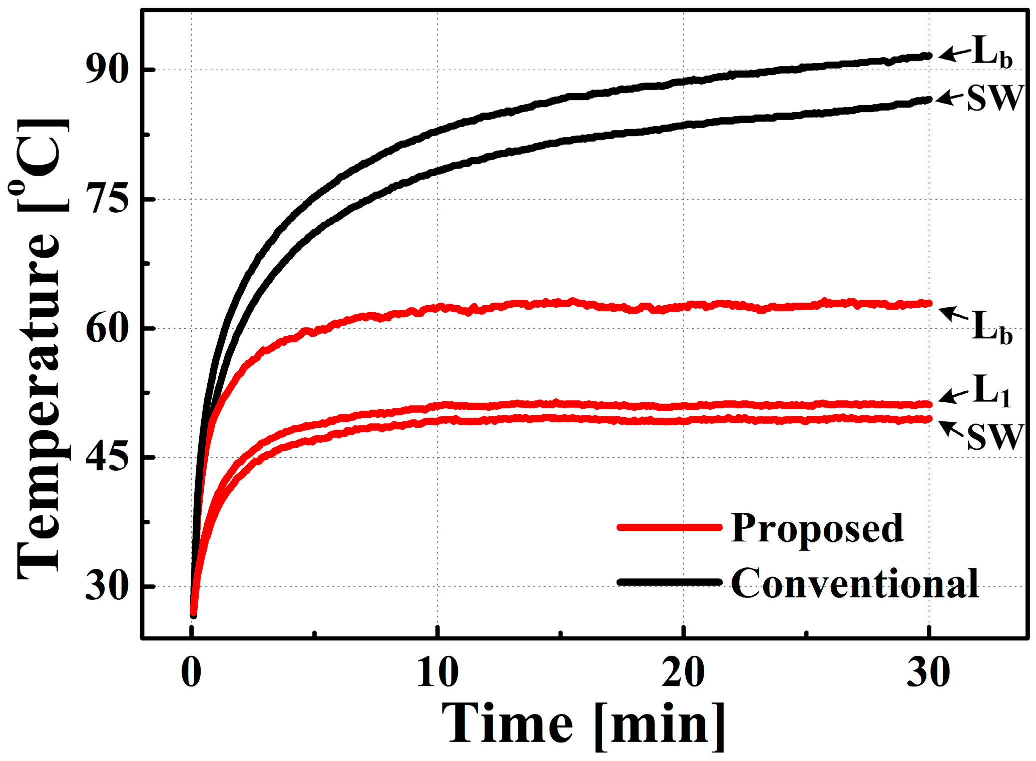
The temperatures of SW and inductors (
Figure 12) were measured for 30 min using a digital temperature recorder (GL-220, GRAPHTEC), while the converters were operated at
VIN = 5 V,
VO = 40 V,
fS = 1 MHz, and
IO = 150 mA. In the conventional boost converter the switch stabilized at 86.6 °C and the inductor stabilized at 91.7 °C, but in the proposed converter, the switch stabilized at 49.5 °C and the inductor stabilized at 62.9 °C. These data indicate that the proposed converter generated less heat loss than the conventional boost converter.
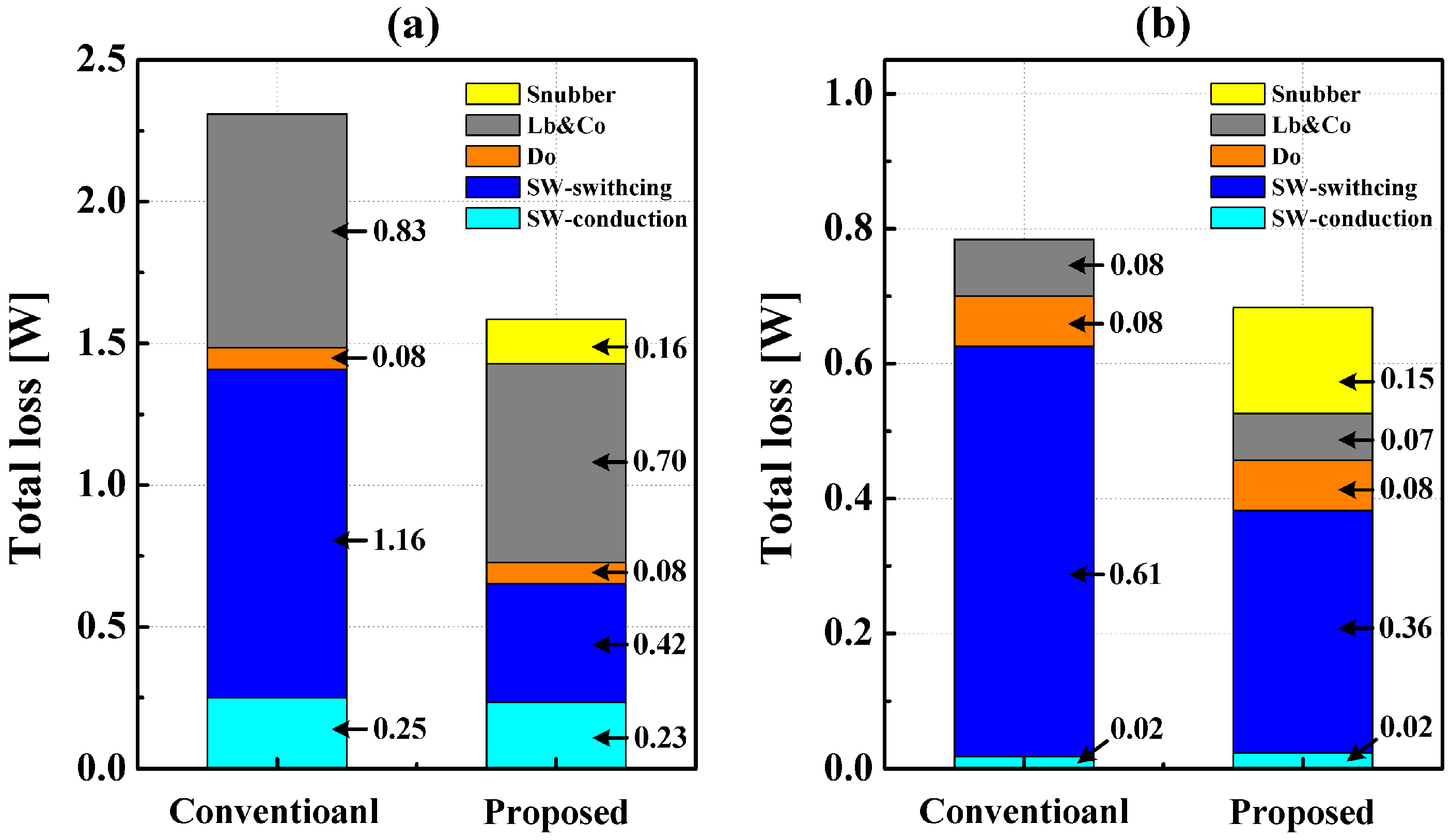
The circuit losses were calculated using a circuit simulator at
VO = 40 V,
IO = 150 mA,
fs = 1 MHz, and
VIN = 5 V (
Figure 13a) and 15 V (
Figure 13b). The total power losses were 1.59 W (proposed) and 2.31 W (conventional) at
VIN = 5 V, and they were 0.68 W (proposed) and 0.78 W (conventional) at
VIN = 15 V. These results show that the proposed converter had lower power loss than the conventional boost converter at both
VIN = 5 V and 15 V. The losses in the switch were 0.65 W (proposed) and 1.41 W (conventional) at
VIN = 5 V, and they were 0.38 W (proposed) and 0.63 W (conventional) at
VIN = 15 V. The proposed converter reduced the switching loss by decreasing
VSW. Additionally, the snubber loss of the proposed converter was 0.16 W at
VIN = 5 V, and it was 0.15 W at
VIN = 15 V. The proposed converter reduced the snubber losses by placing
L1 at the output stage and eliminating the resonant current in the snubber circuit.
The voltage and current stress (
Table 2) of the proposed and conventional boost converter were measured at
VIN = 5 V,
VO = 40 V,
IO = 150 mA, and
fS = 1 MHz. Without parasitic components, the voltage stress of SW and diodes were as follows: (1) in the conventional boost converter,
because
DO was turned ON when SW was turned OFF, and
because SW was turned ON when
DO was turned OFF; (2) in the proposed converter,
because
DO,
D1, and
D2 were turned ON when SW was turned OFF,
because SW was turned ON when
DO and
D1 are turned OFF, and
because
D1 and
DO were turned ON, and SW was turned OFF when
D2 was turned OFF. The proposed converter had lower voltage stress of SW and diodes than the conventional boost converter because
. The current stress of SW was similar in the conventional boost converter and the proposed converter. The current stresses of diodes were lower by half in the proposed converter than in the conventional boost converter.
The voltage stress, current stress, voltage gain, and efficiency of the existing boost converter were calculated using a circuit simulator at
VIN = 5 V,
VO = 40 V,
IO = 150 mA, and
fs = 1 MHz (
Table 3). The efficiency
ηe was 72.6% for the conventional boost converter, 80.4% for the proposed converter, 75.1% for the converter of Reference [
12], and 76.6% for the converter of Reference [
21]. The proposed converter had the highest
ηe for given input and output conditions. The converters of References [
12,
21] had a lower efficiency than that of the proposed converter due to a high current stress and the loss of auxiliary switch, respectively. The voltage stress of the proposed converter was lower than that of the other converters because the voltage stress is
VO-
VC1 in the proposed converter but
VO in the other converters. The current stresses of the proposed converter and the conventional boost converter were similar, but the converter of Reference [
12] had a high current stress because it used resonance to reduce the switching loss at high frequency. At given
VIN and
VO, the proposed converter had the smallest duty, so the proposed converter had the highest voltage gain.


