Abstract
This paper presents a comprehensive investigation on the self-sustained oscillation of silicon carbide (SiC) MOSFETs. At first, based on the double pulse switching test, it is identified that the self-sustained oscillation of SiC MOSFETs can be triggered by two distinct test conditions. To investigate the oscillatory criteria of the two types of self-sustained oscillation, a small-signal ac model is introduced to obtain the transfer function of the oscillatory system. The instability of the oscillation is thereby determined by the two conjugate pole pairs of the transfer function. By analyzing the damping ratios of the two pole pairs, the parametric sensitivity of various circuit and device’s parameters on the two types of self-sustained oscillation are obtained. The analyses reveal the oscillatory criteria of the self-sustained oscillation for SiC MOSFETs. Based on the oscillatory criteria, necessary methods are proposed to prevent the oscillation. The proposed oscillation suppression methods are validated by the experiment at the end of the paper.
1. Introduction
The recent development of fast switching converters require the power switches to operate at a high switching frequency. With high breakdown voltages and fast switching speeds, the silicon carbide (SiC) MOSFETs seem to be a perfect choice for high frequency converter applications [1,2]. However, the utilization of SiC MOSFETs can also introduce some unwanted side-effects to the converter. Under certain test conditions, the self-sustained oscillation can occur in the turn-off transient of SiC MOSFETs [3,4]. As shown in Figure 1, during the oscillatory transient, the gate voltage rings back above the threshold voltage , which gives rise to the the unexpected turn-on of the MOSFET. The unexpected turn-on draws additional energy from the power supply, which compensates the energy dissipated by parasitic resistance in the test circuit. As a results, the oscillation can maintain self-sustenance during the oscillatory transient. Since the self-sustained oscillation causes severe electromagnetic interference (EMI) problems and can completely disrupt the converter operation in the worst case, great care needs to be taken to suppress this kind of oscillation. To achieve this, it is necessary to investigate the underling mechanism and oscillatory criteria of the self-sustained oscillation for SiC MOSFET.
Figure 1.
The self-sustained oscillation waveforms of gate voltage and drain current .
Unfortunately, only few works have been presented to study the self-sustained oscillation phenomenon [3,4,5,6,7]. In [3,4]; with the common source inductance being neglected, the papers studied the sensitivity of various circuit and device’s parameters on the self-sustained oscillation of SiC MOSFETs by casting the switching circuit as the negative conductance oscillator. However, the studies have a few drawbacks. Firstly, since the voltage drop on the inductance can directly affect the gate voltage, the has a very significant impact on the turn-off oscillation. The research proposed in Reference [8] demonstrated that the can disrupt the positive feedback process of the oscillatory system and damp the turn-off oscillation. Under certain test conditions, the can also induce the unexpected turn-on of the low-side MOSFET [7,9] and can excite the self-sustained oscillation during the turn-off transient [7]. Therefore, the inductance should not be neglected in the analysis. Secondly, the potential mechanisms which can lead to the occurrence of the self-sustained oscillation were not revealed in the papers. Last but not least, some circuit parameters, like the stray inductances of gate and power loop, have a very strong impact on the turn-off oscillation [8]. Unfortunately, the parametric sensitivity of these parameters on the self-sustained oscillation were not investigated in the paper. In Reference [5], the self-sustained oscillation phenomenon of a GaN transistor in a half-bridge circuit was studied. The self-sustained oscillation was induced by the unique reverse conduction characteristics of the GaN devices. However, since the SiC MOSFETs do not have such kind of reverse conduction characteristics, the self-sustained oscillation presented in this research does not occur on the SiC MOSFETs. In Reference [6], with the gate-drain capacitance neglected, a simplified SiC MOSFET equivalent model was utilized to derive the transfer function of the oscillatory system. Based on the transfer function, an analytical oscillatory criteria of the self-sustained oscillation was obtained. Since the gate-drain capacitance was neglected, the oscillatory criteria was not very accurate and could only provide an approximate estimation on the occurrence condition of self-sustained oscillation for SiC MOSFETs. In Reference [7], the self-sustained oscillation induced by the the common source inductance was reported for CoolMOS. The research revealed the critical impact of the common source inductance on the self-sustained oscillation. However, the mechanism of the self-sustained oscillation was still unknown. The criteria of the oscillation was also not studied in the paper.
This paper presents a comprehensive study on the potential mechanisms and oscillatory criteria of the self-sustained oscillation for SiC MOSFETs. In Section 2, two distinct test conditions which can trigger the self-sustained oscillation are identified by the double-pulse test. The related positive feedback mechanisms which originate the oscillation are clarified based on the test results. With the common source inductance included, a small-signal ac model is proposed in Section 3 to obtain the transfer function of the oscillatory system. By studying the two pole pairs of the criteria transfer function, the impact of various circuit and device’s parameters on the self-sustained oscillation is analyzed in Section 4. The theoretical analyses reveal the oscillatory criteria of the self-sustained oscillation. The methods to suppress the self-sustained oscillation are thereby obtained in Section 5 according to the oscillatory criteria. In Section 6, the experiment is performed to validate the proposed oscillation suppression methods.
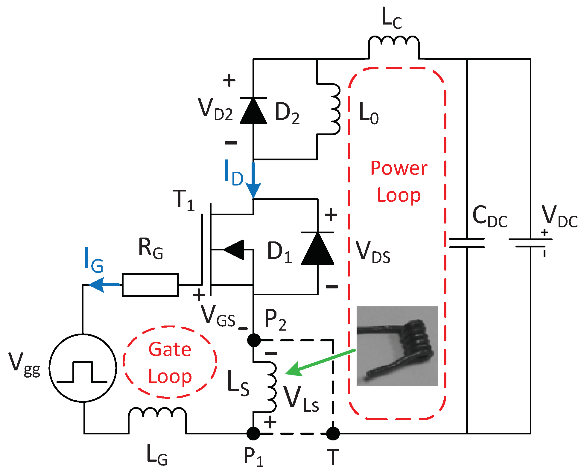
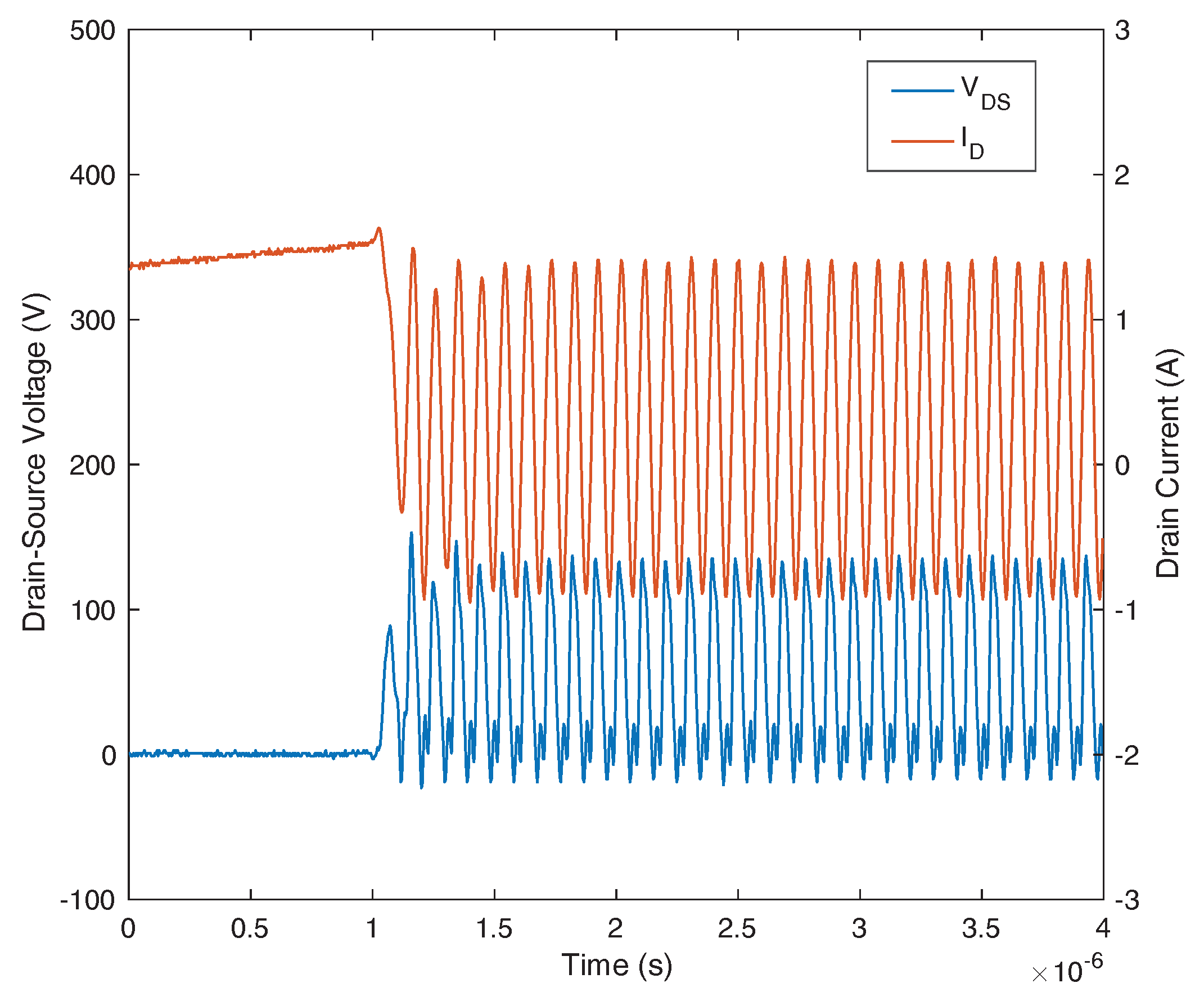
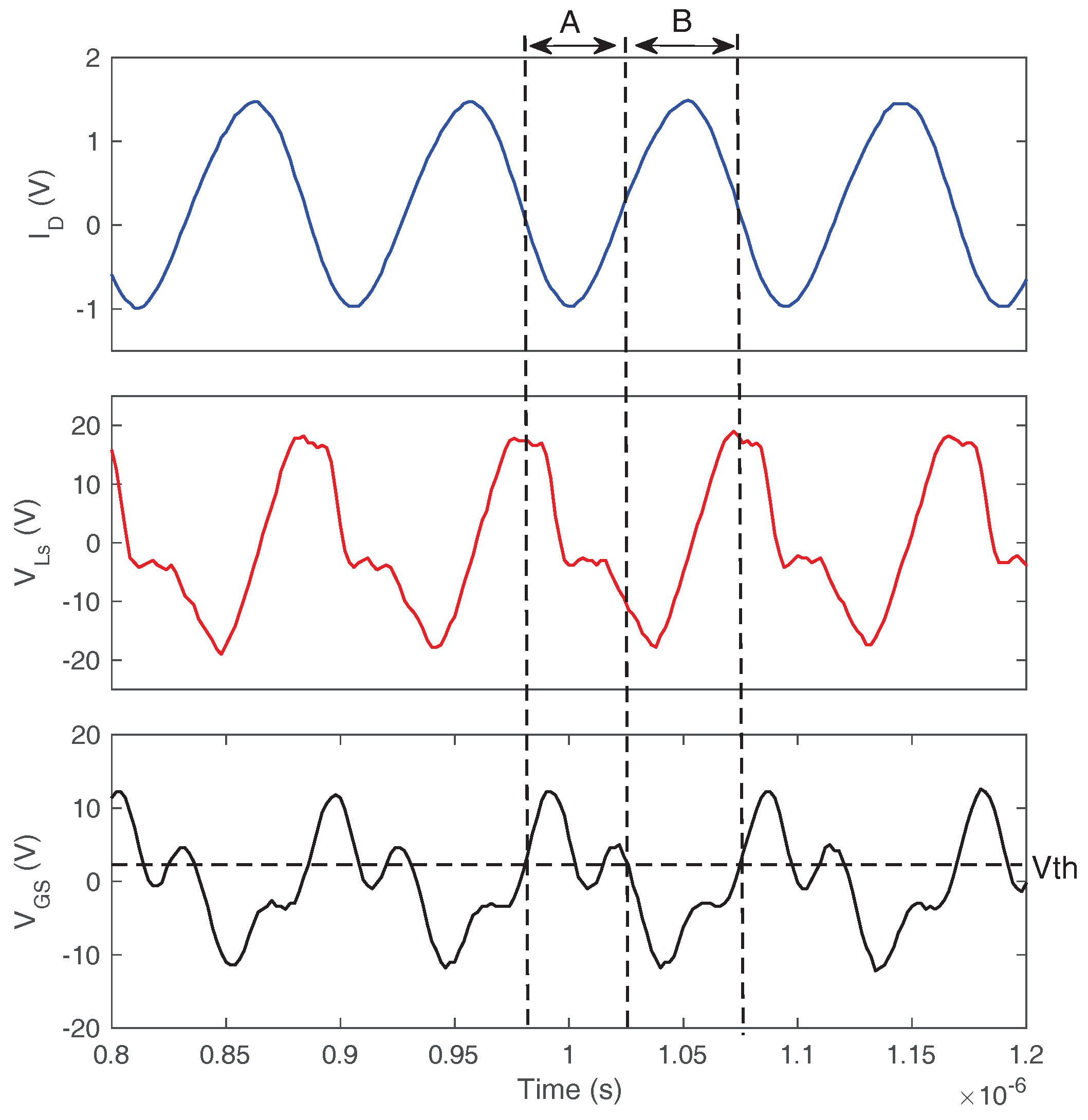
2. Experimental Identification
The double pulse test is utilized to identify the characteristics of the self-sustained oscillation on the 1200V/25A SiC MOSFET with part number LSIC1MO120E0080. A SiC Schottky diode with part number C3D10170H is utilized as the freewheel diode. Figure 2 shows the schematic circuit for the double pulse test. In the circuit, the load inductor H is utilized to maintain a nearly constant current throughout the switching cycle. A function generator is controlled by the computer to send pulse signal to the gate driver, which generates the gate voltage to drive the low-side transistor . is the high voltage power supply, which is connected to a capacitor bank . is the total gate resistance, which is the sum of internal and external gate resistances. is the common source inductance. is the gate loop inductance. is the power loop inductance.
Figure 2.
The schematic circuit of the double-pulse test.
The test results show that the self-sustained oscillation can be excited under two different test conditions depending on the common source inductance . The two types of oscillation are driven by two distinct mechanisms, which are presented as follows.
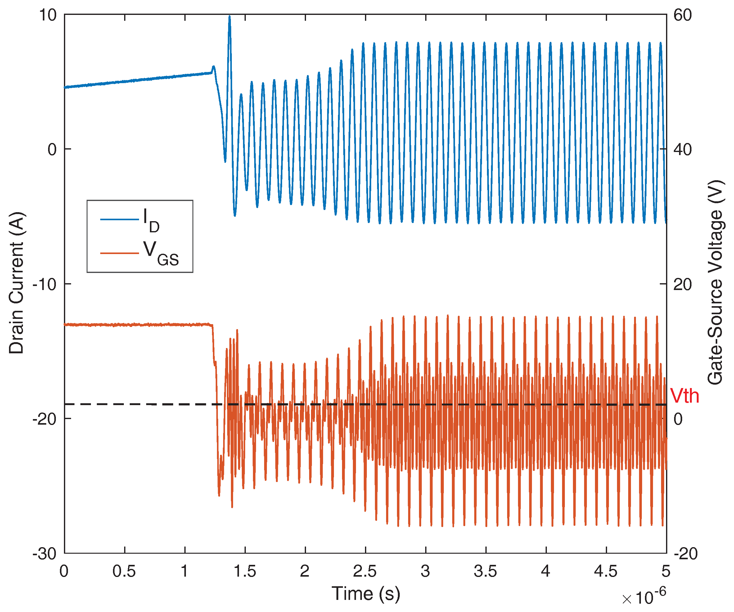
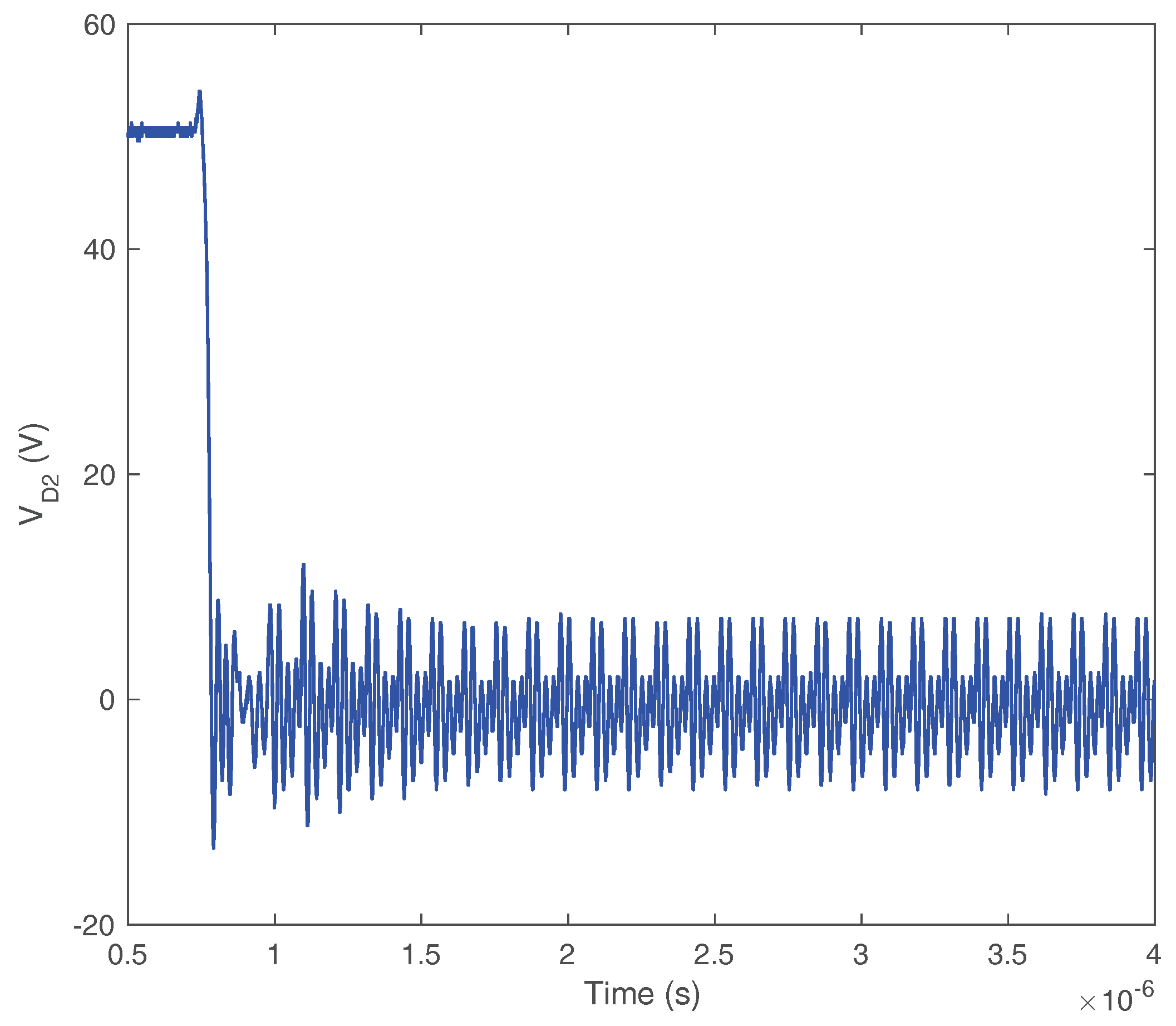
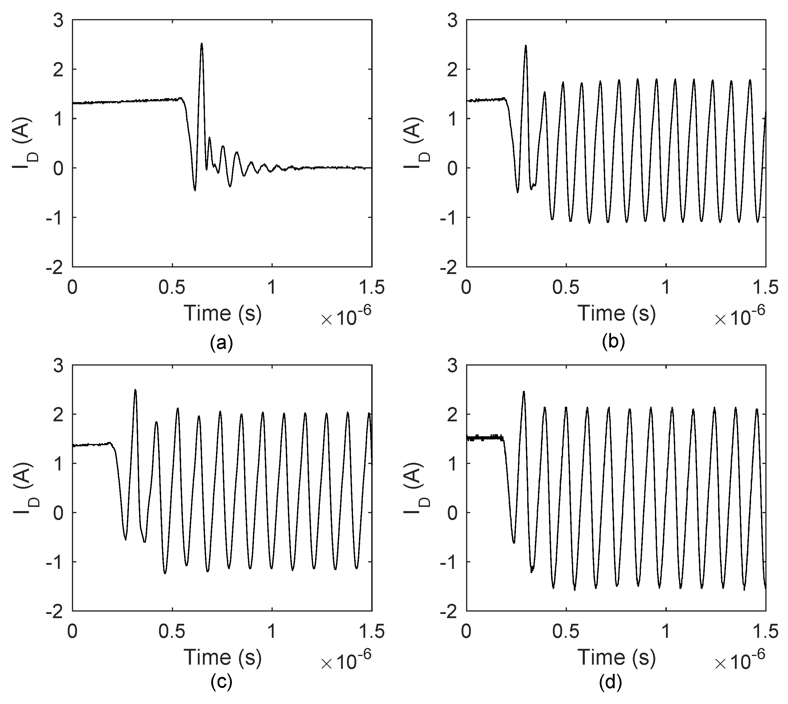
2.1. The Type I Self-Sustained Oscillation
With the node T connected to node , the type I oscillation can be triggered when an air-core coil with an inductance in tens of nanohenries is utilized as , as shown in Figure 2. The type I oscillation waveforms of the and are presented in Figure 3.
Figure 3.
The type I oscillation waveforms of the and (Polarities defined in Figure 2).
To investigate the oscillation mechanism, one oscillation cycle of , , and is divided into phases A and B, as shown in Figure 4. During the oscillatory transient, the voltage on the inductance has the same phase as the , as shown in Figure 4. This demonstrates that the acts as the ac voltage source to drive the gate-source voltage . When the surpasses the threshold voltage in the beginning of phase A, the MOSFET turns on, which give rise to the electron current injection in the drift region. At this time, the depletion region shrinks. Due to the displacement current induced by the discharging of the drain-source depletion capacitance, the still increases reversely in the initiation of this phase. However, since the electron current counteracts the displacement current, the starts to increase and transfers its polarity from negative to positive in the end. With the positive , a negative is generated, which drives the to drop. When the rings down below the in the initiation of phase B, the turns off. Accordingly, the depletion region starts to expand. Due to the displacement current generated by the charging of drain-source depletion capacitance, still increases. However, with the great reduction of the MOS electron current, the starts to decline and eventually transfers back into a negative value. Accordingly, a positive is obtained, which drives the to increase. When the achieves at the end of the phase, phase A starts again. As a result, the two phases occur alternatively and the self-sustained oscillation is generated.
Figure 4.
The type I oscillation waveforms of , , and (Polarities defined in Figure 2).
It should be noted that an underling positive feedback mechanism is included in the oscillation process presented above. During the oscillatory transient, the oscillation of generates the ac voltage . drives the MOSFET turn-ons and -offs, which in return supports the oscillation of . This gives rise to the positive feedback process, which excites the type I oscillation. This common source inductance-induced oscillation phenomenon has been reported previously in Reference [7] for the CoolMOS.
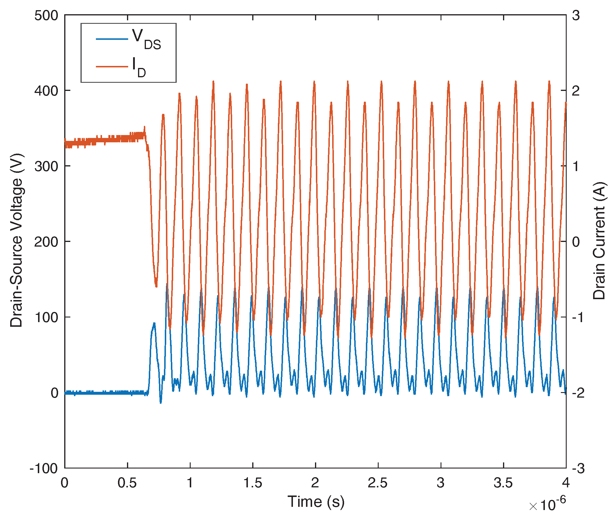
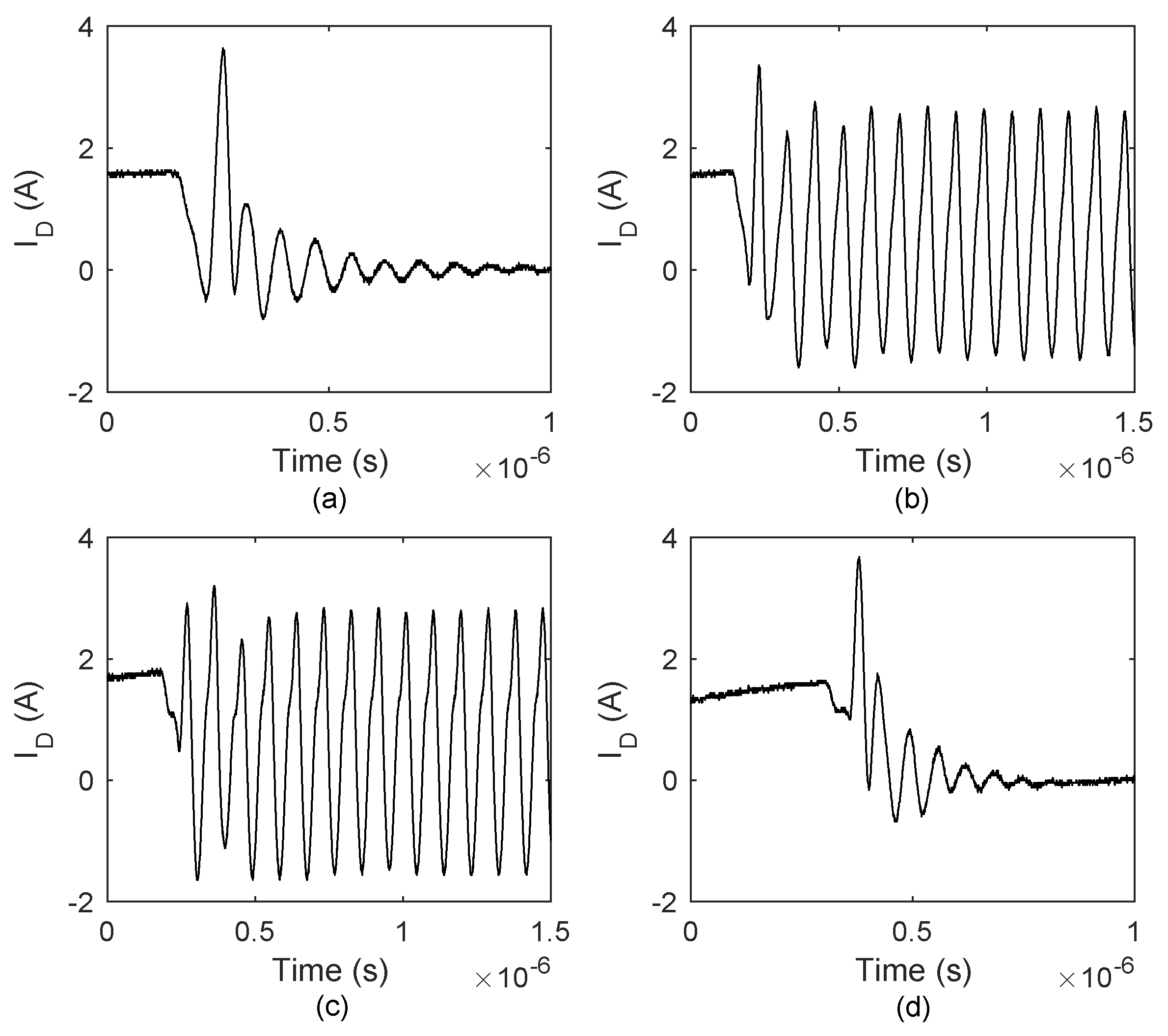
2.2. Type II Self-Sustained Oscillation
When the node T is connected to node (the end of the source lead), the common source inductance is minimized. In this scenario, the type II self-sustained oscillation can be triggered, as shown in the Figure 5.
Figure 5.
The type II oscillation waveforms of and .
To investigate the mechanism of the type II oscillation, one oscillation cycle is divided into phases A and B, as shown in Figure 6. In phase A, the drops down below the threshold voltage , MOSFET turns off. At this time, the drift layer is depleted, which gives rise to a very small gate-drain capacitance . Since the high impedance of isolates the gate loop from being affected by the power loop resonance, and oscillate due to the resonance of gate loop RLC circuit. When rings back above the , phase B starts. In this phase, the MOSFET turns on. The shrinking of the depletion region gives rise to the great increase of the . With a much larger , the power loop resonance can disturb the gate loop resonance. As shown in Figure 6, the gate current increases abruptly a short time after the initiation of phase B and quickly becomes in phase with the drain current . This demonstrates that a portion of the drain current serves as a feedback current flows though the gate drive circuit, as shown Figure 7. This current feedback action induces the abrupt increase of . With a high , a positive voltage is generated on the , as shown Figure 7. The positive can drive the gate voltage , which in turn supports the drain current . As a result, a positive feedback process is generated. The type II oscillation thereby occurs. The self-sustained oscillation studied in Reference [3,4] is a type II oscillation.
Figure 6.
The type II oscillation waveforms of , , and (Polarities defined in Figure 2).
Figure 7.
The current feedback process in phase B.
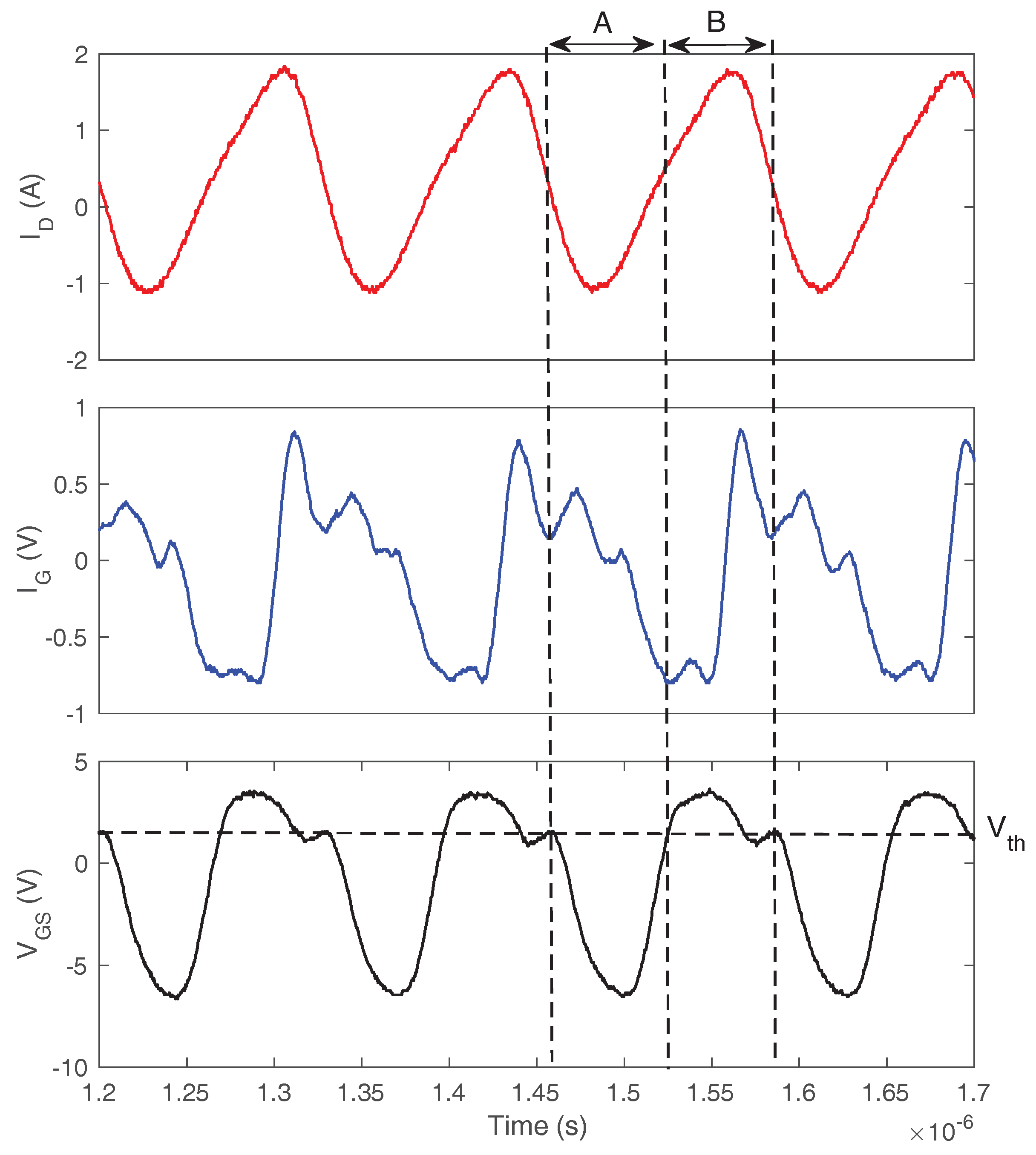
2.3. The Impact of on Self-Sustained Oscillation
Traditionally, the turn-off oscillation is supposed to be triggered by the high [8,10]. In this test, it is found that does not have a significant influence on the two types of self-sustained oscillation. As shown in Figure 8, the self-sustained oscillation can be excited when the load current reduces from 10 A to 1.5 A. In fact, since does not have a significant impact on the positive feedback mechanisms which trigger the two types of self-sustained oscillation, the occurrence of self-sustained oscillation do not rely on the high .
Figure 8.
The oscillation waveforms of for type I (blue) and type II (red) self-sustained oscillation. (a) A. (b) A. (c) A. (d) A.
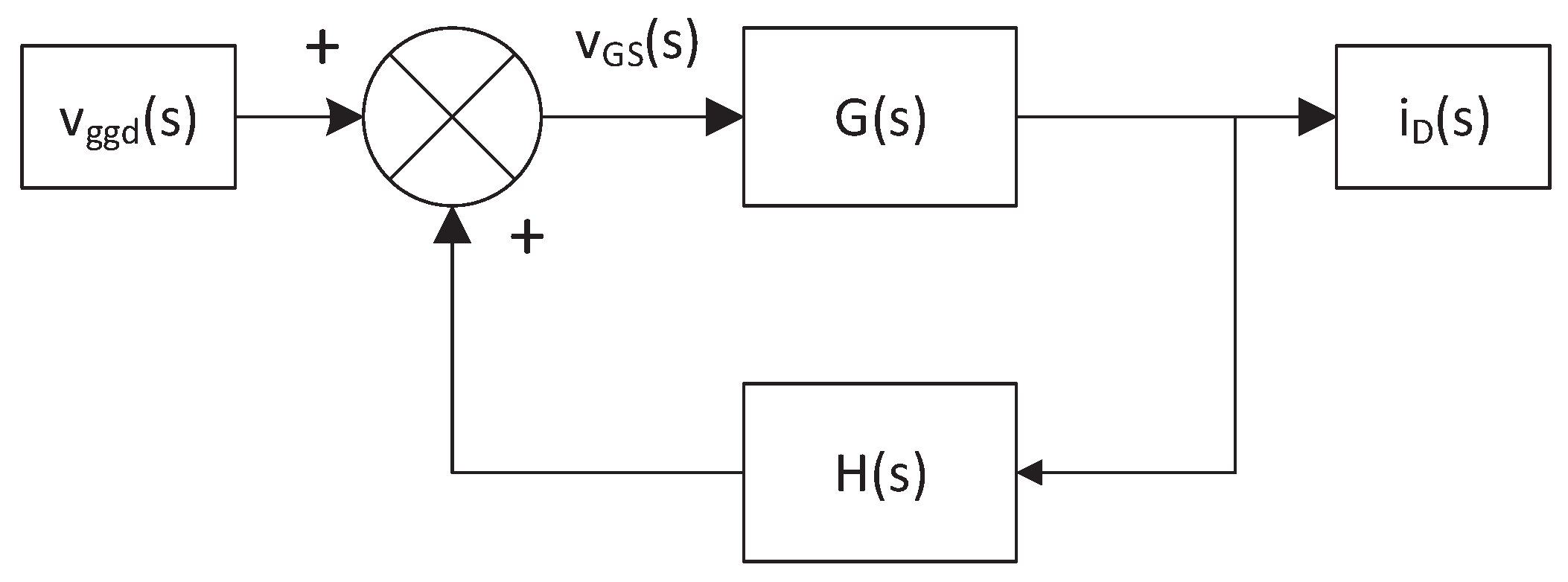
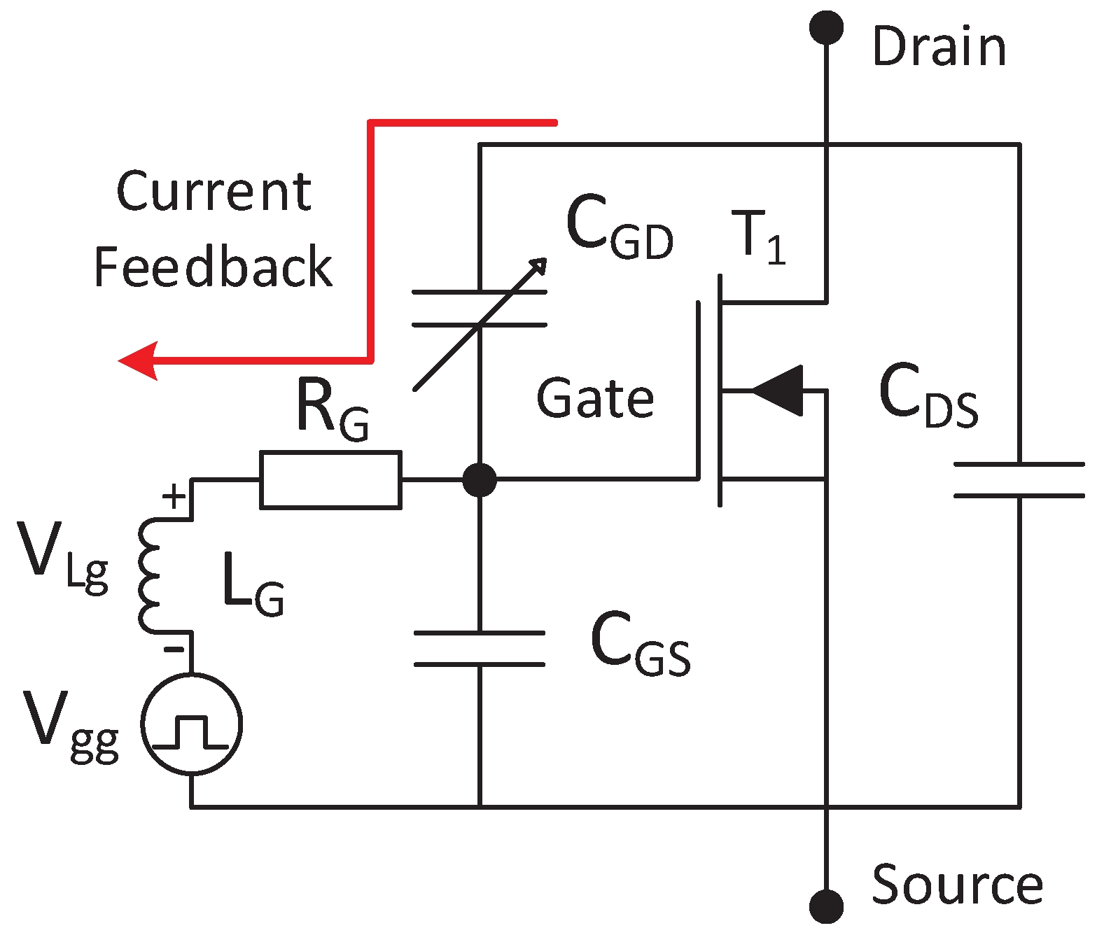
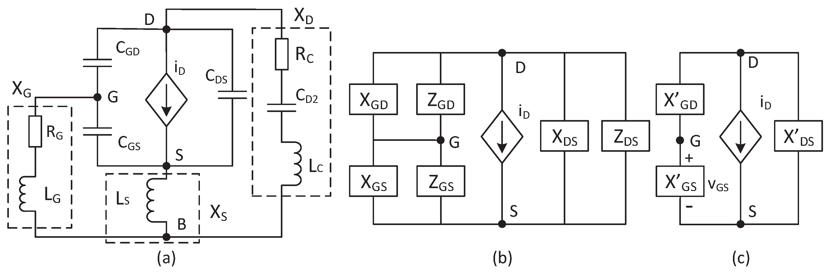
3. The Small-Signal Ac Model
The instability of the self-sustained oscillation can be studied by the small-signal ac model [3,4,5]. To obtain the model, the test circuit presented in Figure 2 is transferred to the equivalent small-signal circuit shown in Figure 9a. In the circuit, the capacitor and voltage supply are short circuited. The diode is replaced as the diode junction capacitance . The transistor is replaced by its equivalent small-signal model. In the model, , , and are the gate-drain, drain-source, and gate-source capacitances, respectively. is the stray resistance of power loop. is a small-signal MOS current. is the small-signal gate-source voltage. is the transconductance of the power MOSFET. In order to simplify the equivalent circuit, the star connection at the node B is transformed to delta connection with the following equations:
where , , . As a result, the initial small-signal model presented in Figure 9b can be obtained. In the model, , and . After further simplification, the final small-signal model can be drawn, as shown in Figure 9c. In the model, , and .
Figure 9.
An equivalent ac model of the test circuit. (a) An equivalent small-signal circuit. (b) The initial small-signal model. (c) A simplified small-signal model.
During the oscillatory transient, the small-signal model can be considered as single-input single-output feedback system [5,11]. Figure 10 shows the block diagram of the feedback system. The and are the Laplace transform of the and , respectively. is the Laplace transform of the pulse form small-signal disturbance voltage , which is introduced by the gate drive voltage. It should be noticed that the gate drive voltage is constant when the gate drive switches off. Therefore, the small-signal becomes zero after the initial voltage disturbance. The instability of the oscillation is thereby determined by the feedback system, not the input signal . The open-loop gain of the feedback system is as follows:
Figure 10.
The positive feedback block diagram.
The feedback factor can be calculated by the small-signal model presented in Figure 9c:
The closed-loop transfer function of the feedback system thereby can be obtained:
where the coefficients and (i = 0,1,2,3,4) are presented in the Appendix A.
It should be noted that the dc operating point utilized for the small-signal model is included implicitly in Equation (4). In the model, the capacitances and are the functions of the drain-source voltage . The capacitance is the function of diode voltage . The transconductance is the function of gate-source voltage . During the turn-off transient, the central tendency of the oscillation is the voltage supply . The capacitances and are thereby linearized at . During the oscillatory transient, the freewheel diode is forward biased when the MOSFET turns off. When the turns on, the diode has to support the reverse voltage. Therefore, the diode voltage oscillates around the zero volts, as shown in Figure 11. The is thereby linearized at V. Following the approach presented in Reference [3,11], the transconductance is linearized at .
Figure 11.
The waveforms of (Polarities defined in Figure 2).
4. The Analysis of Parametric Sensitivity on the Oscillatory Instability
The stability of the oscillation can be studied by the poles of the closed-loop transfer function . According to the well-known Routh–Hurwitz stability criterion, the oscillation is instable when the system has a conjugate pole pair at the right half of the s-plane [12]. In this case, the transfer function has two complex conjugate pole pairs. The loci of the two pole pairs and when the common source inductance varies from 0 nH to 40 nH are presented Figure 12. The specific parameters utilized in the analysis are presented in Table 1.
Figure 12.
The loci of the conjugate pole pairs when varies from 0 nH to 40 nH.
Table 1.
Parameters for the theocratical study.
As shown in Figure 12, when becomes larger, the pole pair moves toward the right and reaches the right half of the s-plane when is larger than 10 nH. Since the type I self-sustained oscillation is induced by the large , the occurrence of the type I oscillation is thereby determined by . The pole pair , on the other hand, moves toward the opposite direction as and lies on the right half of the s-plane when is eliminated. This shows that pole pair dictates the occurrence of type II oscillation. The parametric sensitivity of the two types of self-sustained oscillation can be studied by the two pole pairs.
In this section, the instability of the oscillation is described by the damping ratio , where − and are the real and imaginary parts of the poles. When , the oscillation is instable and the smaller the is, the faster the oscillation amplitude increases. When , the oscillation is stable. With a larger , the oscillation will return to equilibrium faster. indicates a constant-amplitude oscillation.
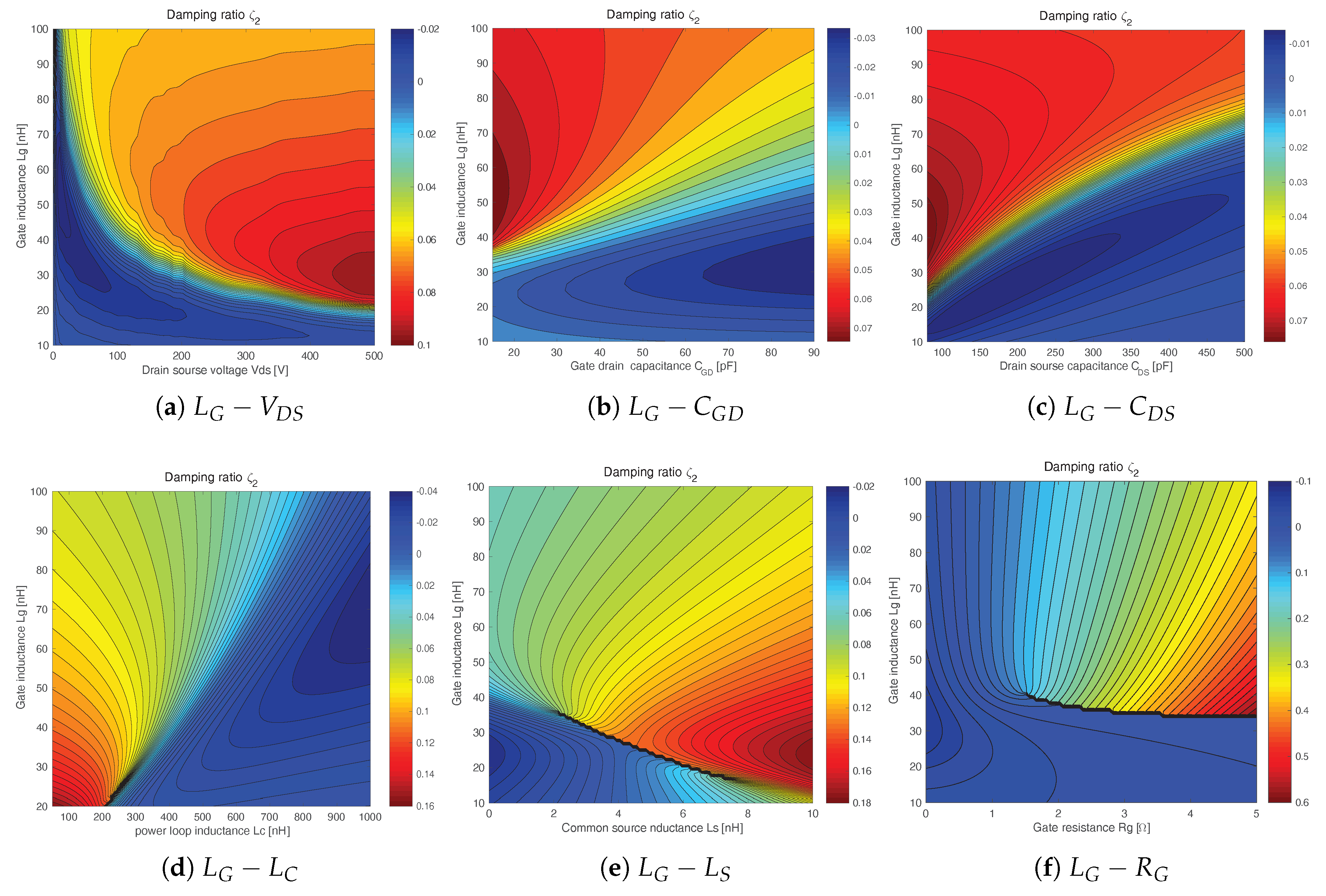
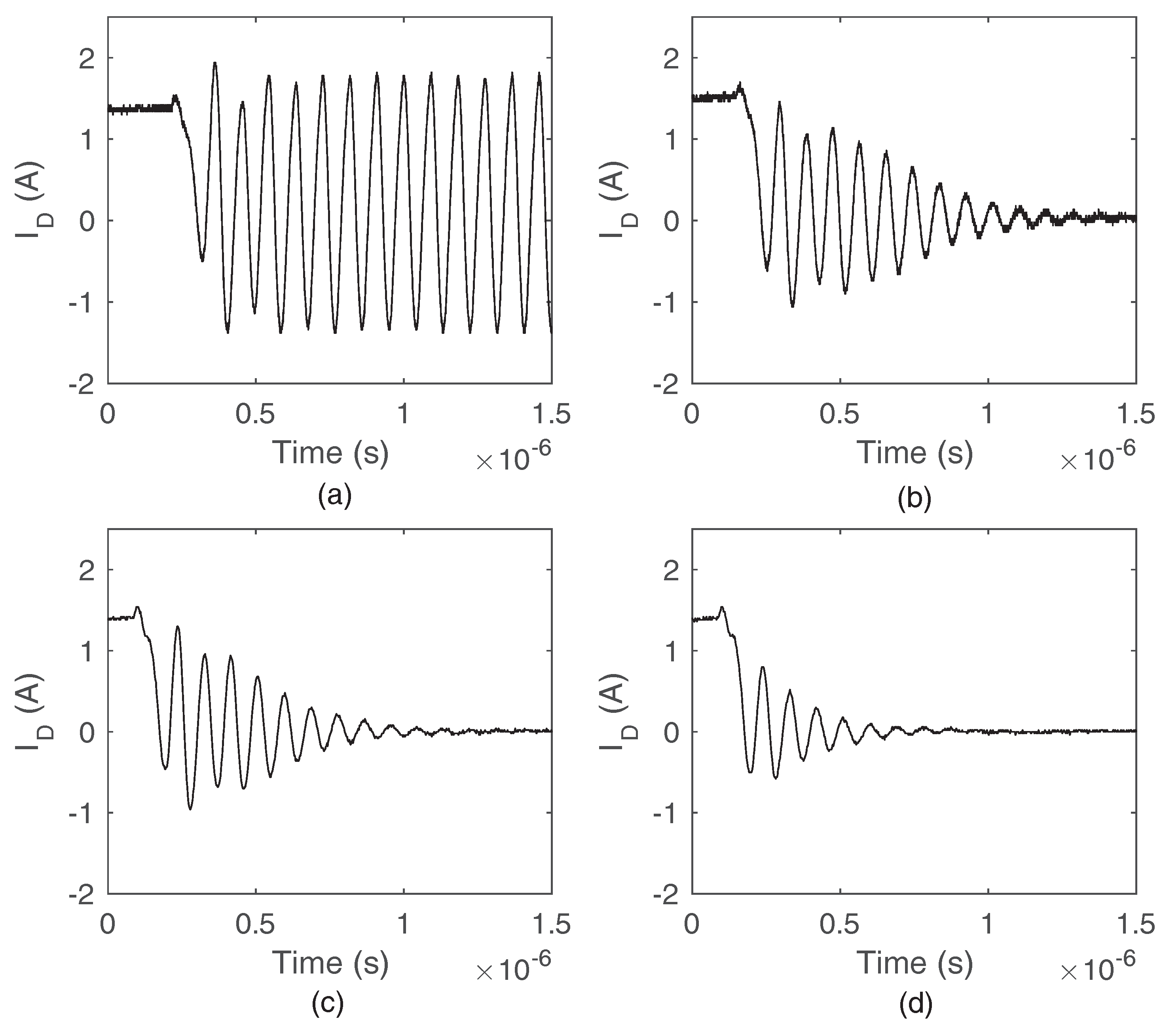
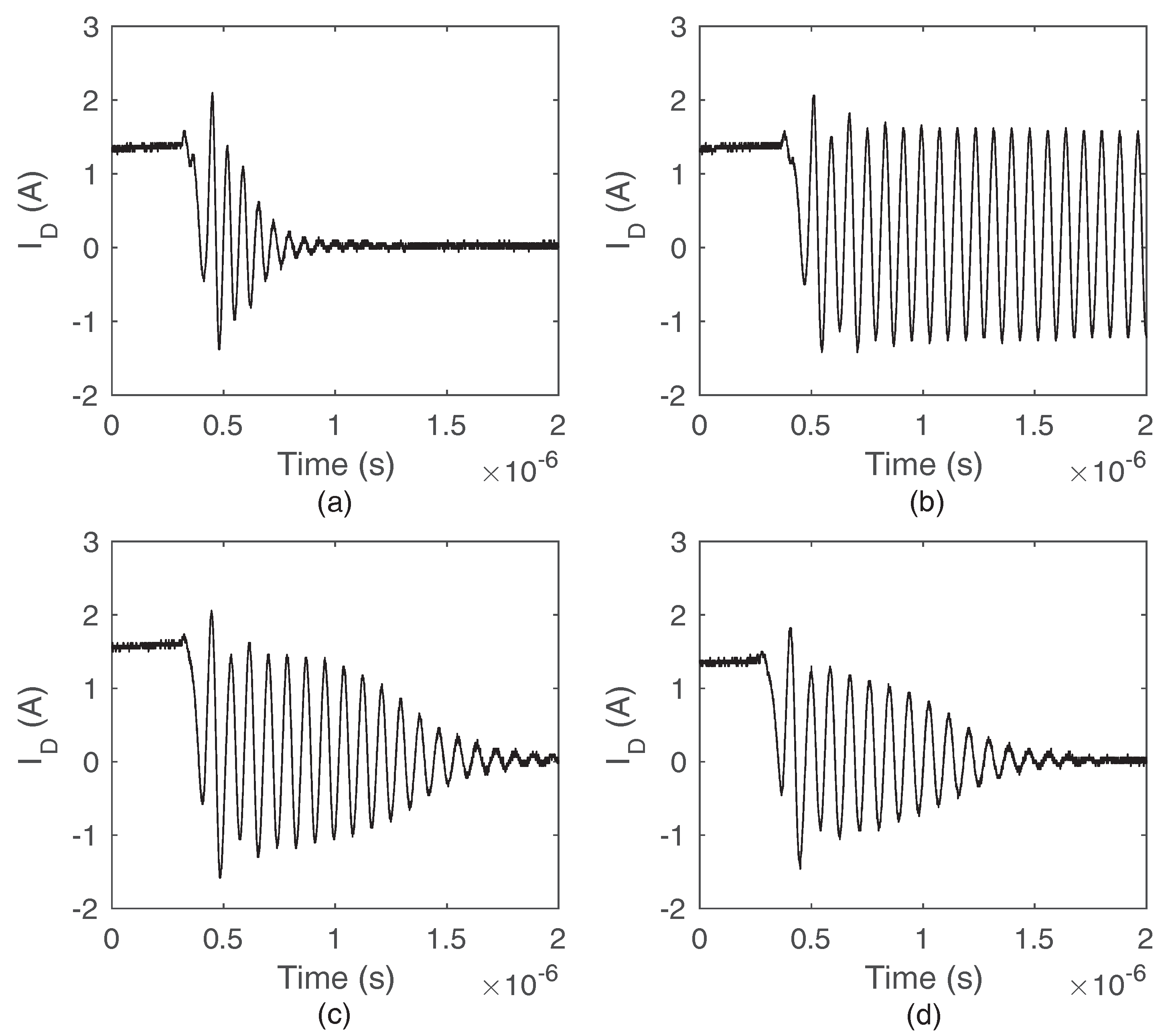
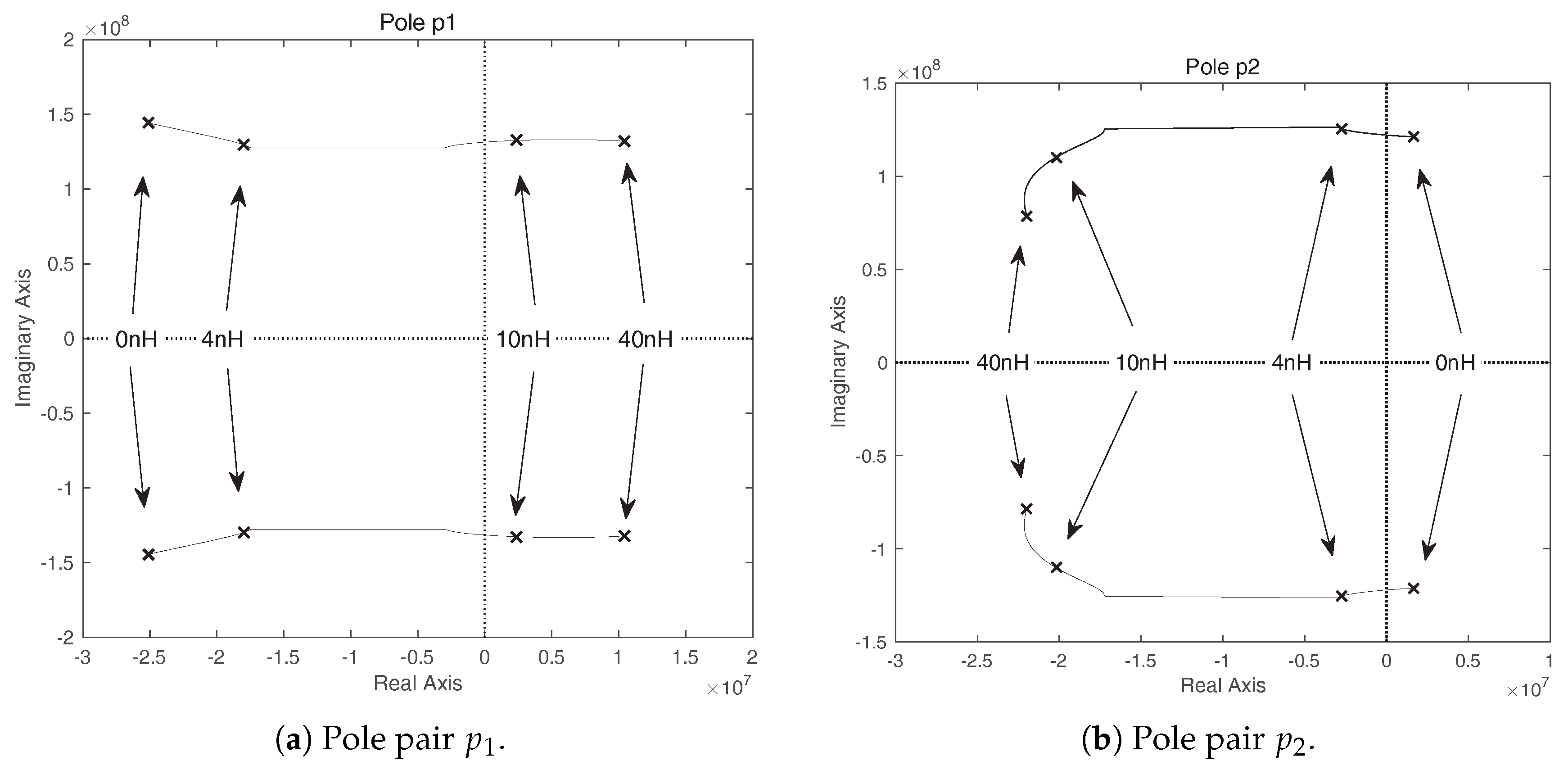
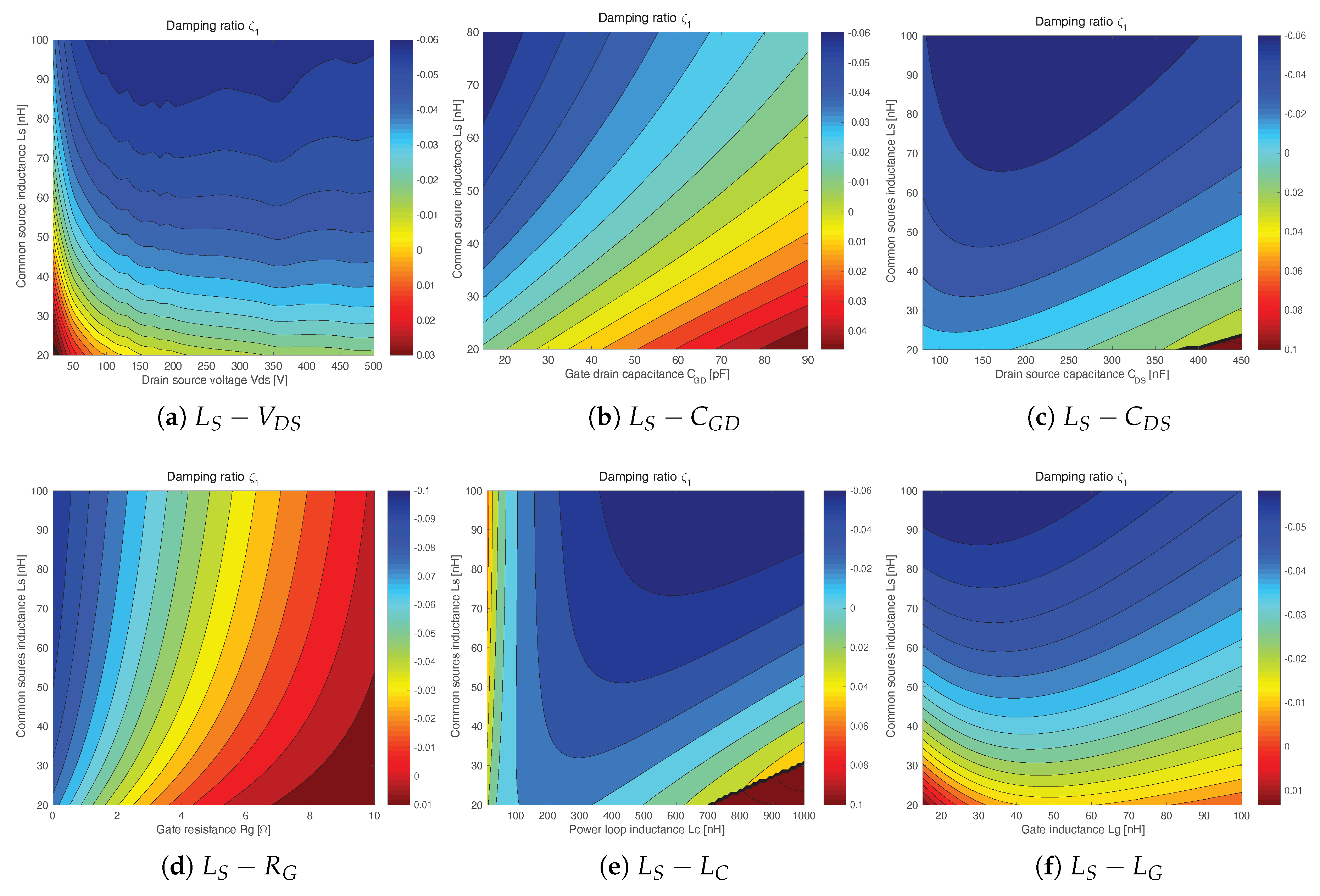
4.1. The Parametric Sensitivity of the Type I Oscillation
In this subsection, the damping ratio of pole pair is calculated to study the oscillatory criteria and the parametric sensitivity of the type I oscillation. The portion has as the instable region which is susceptible to the self-sustained oscillation. The parameters in Table 1 are utilized to calculate with , and varies from 20 to 100 nH. It should be noted that and also vary when the supply voltage changes. The and curves are extracted from the device’s datasheet.
According to the oscillation mechanism presented in Section 2, the type I oscillation is driven by a common source inductance . With a larger , a higher oscillation amplitude can be obtained on to excite the gate voltage oscillation. As a result, the positive feedback process is enhanced and the oscillatory system becomes more instable. Figure 12a has already demonstrated that the type I oscillation is driven by the . This can also be validated by the damping ratio . As shown in Figure 13, the decreases significantly with the increase of .
Figure 13.
The calculated damping ratio .
The impact of the on the damping ratio is presented in Figure 13a. With the increase of the , the damping ratio has a short-term initial reduction and then approximately remains constant when is larger than about 150 V. The initial reduction of is due to the decrease of the capacitance and , as shown in Figure 13b,c. When reduces to about 150 pF (approximately corresponding to 150 V of ), starts to increase with the reduction of , as shown in Figure 13c. Since it counteract the damping ratio decrease induced by a reduction of , approximately remains constant with the increase of the when V.
As shown in Figure 13d, the gate resistance has a significant damping effect on type I oscillations. Few ohms of can completely suppress the oscillation. Since can damp the gate loop resonant and break down the feedback process, the damping effect is obvious. Figure 13e shows the impact of power loop parasitic inductances on the type I oscillation. When has a small value, the common source inductance greatly loses its driving force and has no significant impact on the damping ratio. At this time, the greatly decreases with the increase in . When becomes large enough, regains its driving force and becomes the dominant factor in determining the damping ratio . At this time, the only increases slowly with the raise of the . The impact of greatly depends on the value of . In order to reduce the driving force of the , should be as small as possible. The gate inductance , on the other hand, has a much subtler influence on the damping ratio. As shown in Figure 13f, with the raise of , the only slightly decreases at first and then undertakes a slow rising in the end. is an insignificant factor for type I oscillations.
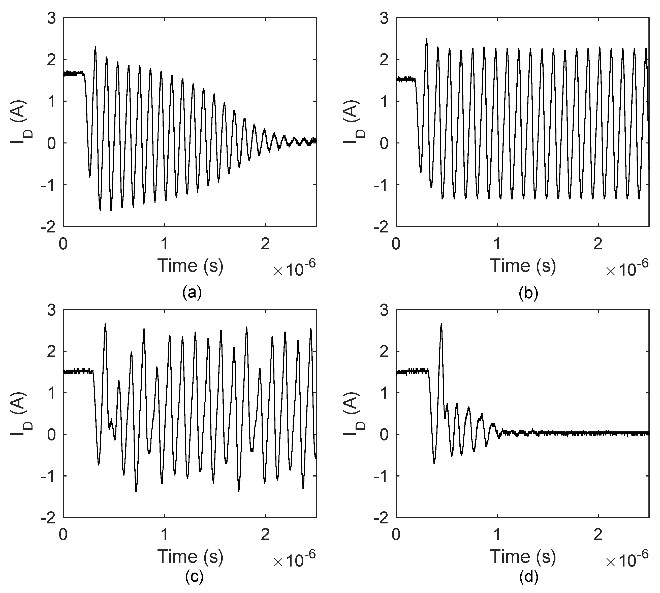
4.2. The Parametric Sensitivity of the Type II Oscillation
In this subsection, the damping ratio of pole pair is calculated to identify the oscillatory criteria and parametric sensitivity of a type II oscillation. The parameter set presented in Table 1 is utilized with nH, and varies from 10 to 100 nH.
Figure 14 shows the influenced of on the damping ratio . With the raise of , the damping ratio decreases at first and then quickly increases to a large positive value at the boundary of the instable region. This phenomenon can be explained by the type II oscillation mechanism presented in Section 2: A slight increase in can generate a higher voltage to drive the gate voltage. This enhances the positive feedback process, and the oscillatory system becomes more instable. However, if is too large, its high impedance can also hinder the drain current feedback process. The oscillation is thereby greatly suppressed.
Figure 14.
The calculated damping ratio .
Figure 14a presents the impact of on the . As shown in Figure 14a, with the increase in , the instable region is greatly compressed. When is large enough, the instable region totally vanishes. In the instable region, the minimum damping ratio and the which achieves the minimum decrease with the increase of . This phenomenon is due to the variation of the parasitic capacitances. As shown in Figure 14b,c, with the reduction of and , the similar variation tendency of is evident.
The influence of the inductance on the damping ratio is presented in Figure 14d. When the has a small value, the oscillation is completely suppressed. decreases with the raise of . When becomes enough large, the instable region starts to form and greatly expands with the increase of . The minimum value of in the instable region decreases with the increase of . In the vicinity of lower boundary of the instable region, the damping ratio slightly rises with the increase of . Therefore, to minimize the instable region, the should be as small as possible. The inductance shows a very strong damping effect on the oscillation system. As shown in Figure 14e, with few nanohenries of , a very large damping ratio can be achieved. At this time, the phase of the voltage across is opposite the gate-source voltage [8,13]. This provide negative feedback to the oscillatory system [8], which significantly dampens the turn-off oscillation [14]. The impact of gate loop resistance on the damping ratio is shown in Figure 14f. The resistance shows a significant damping effect on a type II oscillation. Since the resistance dampens the gate loop resonate, the damping effect is reasonable.
5. Oscillation Prevention
Based on the analyses presented in the previous section, the methods which can prevent a type I oscillation are summarized as follows:
- (1)
- Reducing the inductance : Since voltage on the is the major driving force of type I oscillations, the reduction of can greatly reduce and suppress type I oscillations.
- (2)
- Reducing the inductance : As shown in Figure 13e, the damping ratio significantly increases with the reduction of . can greatly lose its driving force when is small enough. Therefore, the reduction of is a very effective way to suppress type I oscillations.
- (3)
- Increasing the gate resistance : As shown in the Figure 13d, the damping ratio greatly increases with the raise of . Increasing is an obvious choice to avoid the self-sustained oscillation.
To suppress type II oscillations, the necessary measures which should be adopted are summarised as follows:
- (1)
- Reducing the inductance : With the reduction of , the instable region significantly compresses, as shown in Figure 14d. When is small enough, the type II oscillation can be eliminated.
- (2)
- Optimizing the gate inductance : The gate inductance has a great impact on type II oscillations. Many researches on the gate driver design claim that the gate driver should be very close to the MOSFET to avoid oscillations induced by the large [15,16]. Reducing is supposed to be the primary way to suppress the switching oscillation [8]. However, in this study, the analyses presented in Figure 14a,d reveal that the reduction of does not necessarily suppress type II oscillations. Its influence greatly depends on the operating condition, which is determined by parameters like and . Therefore, to suppress a type II oscillation, the value should be carefully chosen based on the operating condition.
- (3)
- Increasing the gate resistance : As shown in Figure 14f, the gate resistance has a very strong damping effect on the type II oscillation. Few ohms of are able to completely suppress the oscillation.
- (4)
- Increasing the supply voltage : Since the oscillation is biased by the supply voltage , the increase of can elevate the central tendency of the oscillation. As shown Figure 14a, with a high , a type II oscillation can be suppressed.
It should be noted that increasing can also greatly suppress a type II oscillation. However, a large will significantly slow down the switching speed [8], which induces higher switching losses [17]. Moreover, a type I oscillation can also be triggered by the large . Therefore, increasing is not a very good option for oscillation suppression.
6. Experimental Validation
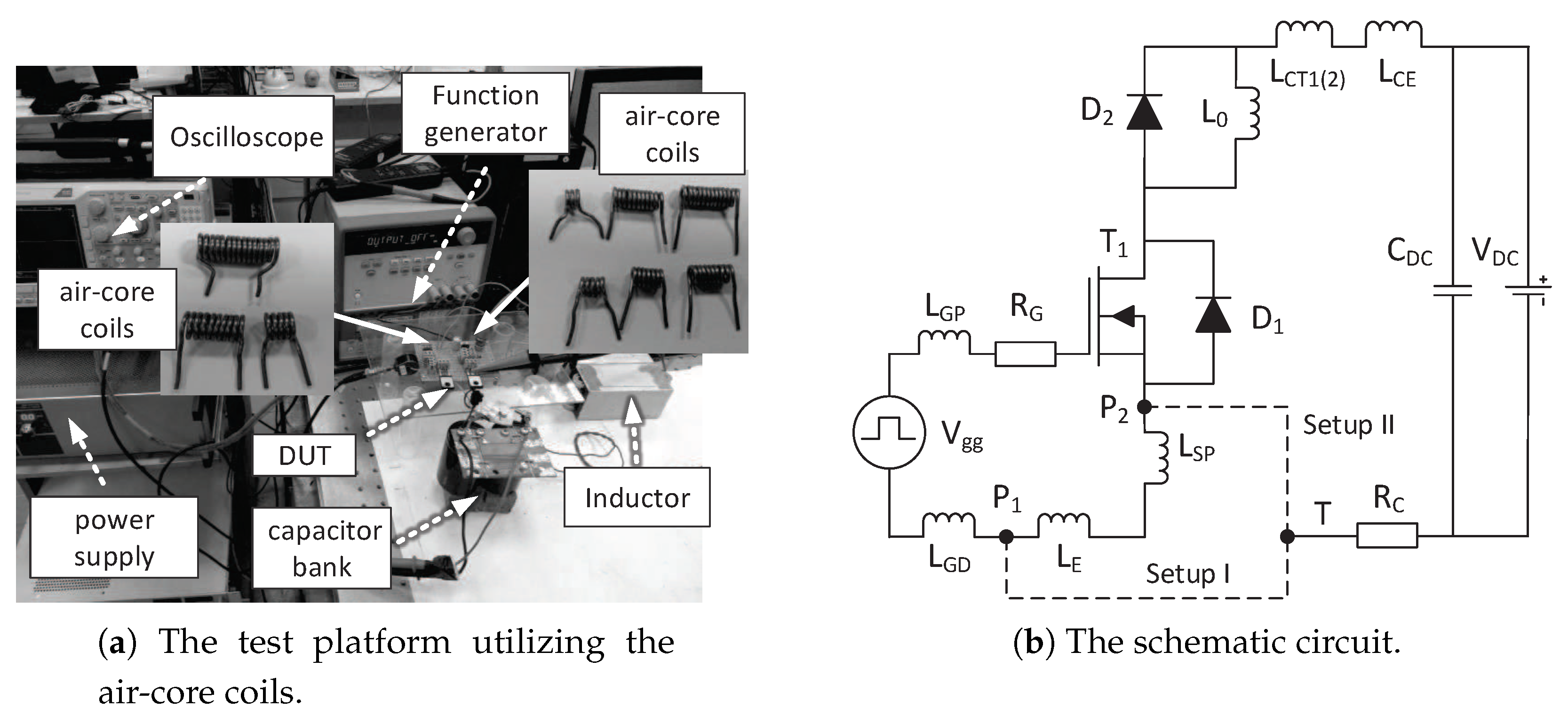
6.1. Experiment Setup
The double pulse switching test is performed to verify the oscillation suppression methods presented in the previous section. In the test, to ensure the safety of the gate driver and the DUT, the load current is 1.5 A. This is a reasonable setup, since Figure 8 has already demonstrated that the load current does not have a significant impact on the occurrence of self-sustained oscillation. The supply voltage is 50 V, which also varies from 50 V to 300 V to validate the influence of on a type II oscillation. Figure 15 shows the test platform and the schematic circuit for the test. In the test circuit, setups I and II are utilized to trigger the two type oscillation and various air-core coils are utilized to change the inductance of , , and . As shown in Figure 15b, and are the stray inductances of the double-pulse tester for setup sI and II, respectively. The inductances of and can be extracted by following the method presented in Reference [18]. and are the external air-core coils utilized in the power and gate loops. Their inductances are extracted by the method presented in Reference [19]. The power loop inductance . and are the source and gate package stray inductances. is the parasitic inductance of the gate drive circuit. The inductances of , , and are extracted by the Q3D extractor. The power loop parasitic resistance is directly measured in the circuit. The parameters of the SiC MOSFET and schottky diode are extracted from the datasheet based on the dc operating point. All the parameters utilized in this validation are summarized in Table 2.
Figure 15.
The test platform and the schematic circuit with air-core coils.
Table 2.
Parameters for the validation.
6.2. Experiment Results
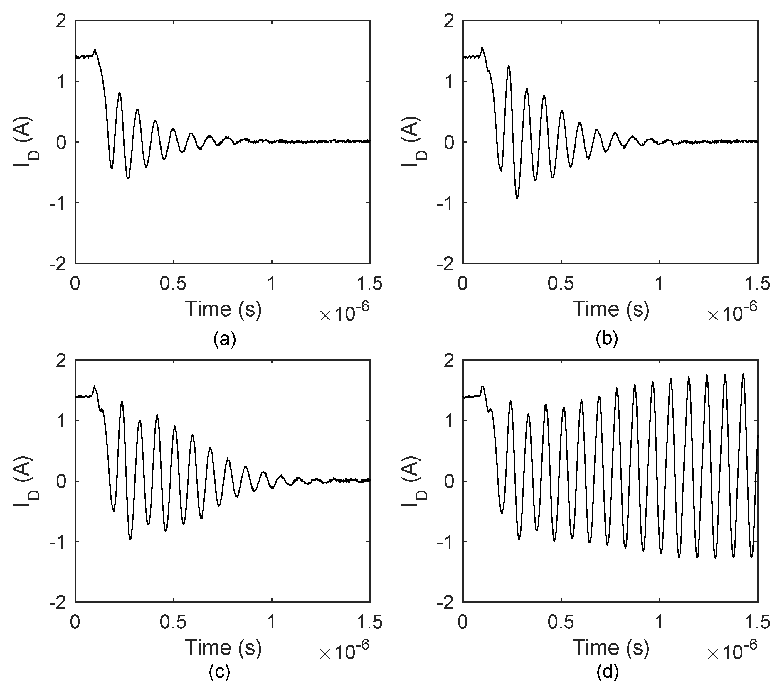
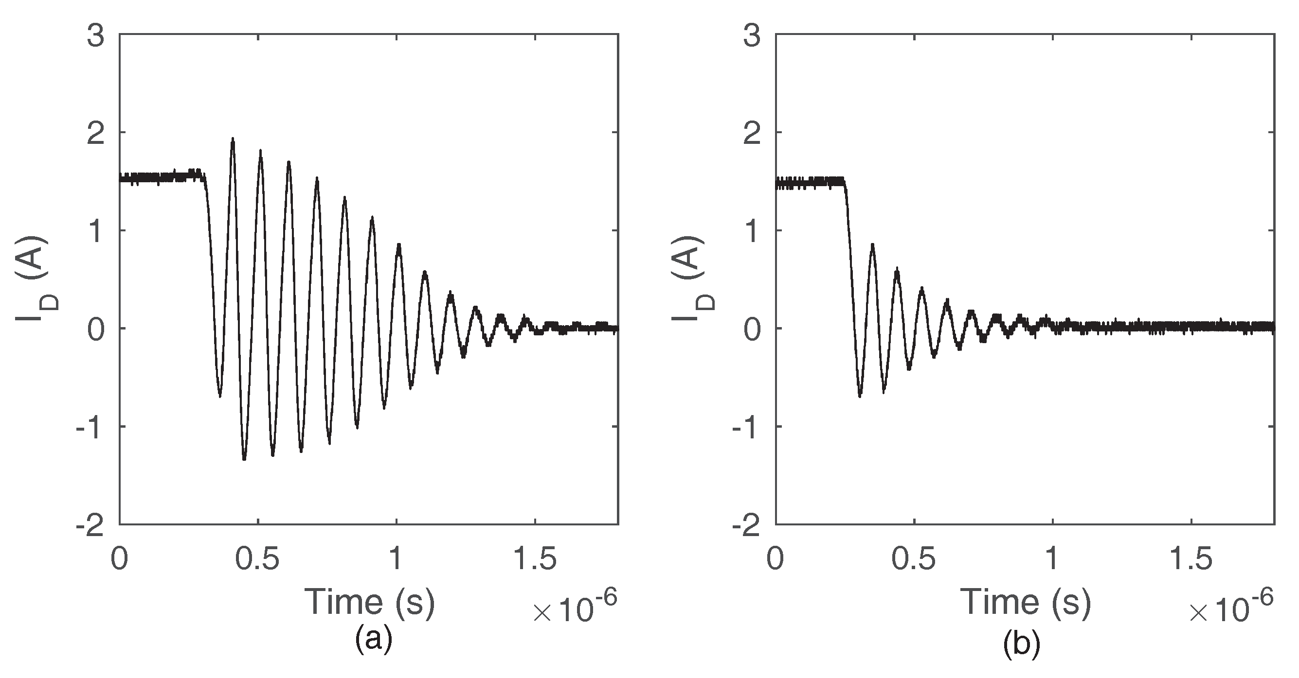
6.2.1. Type I Oscillation
In order to obtain a large to trigger a type I oscillation, node T is connected to node , as shown the setup I in Figure 15b. In this scenario, nH and . Table 3 shows the number of oscillation cycles and the damping ratio with various and for the type I oscillation. Figure 16 and Figure 17 present the corresponding experimental waveforms. The self-sustained oscillation cycles is marked as “inf” in Table 3.
Table 3.
A comparison between the and number of oscillation cycles (bold) with various and with nH.
Figure 16.
The experimental type I oscillation waveforms of the drain current with various with and nH. (a) nH. (b) nH. (c) nH. (d) nH.
Figure 17.
The experimental type I oscillation waveforms of the drain current with various with nH and nH. (a) . (b) . (c) . (d) .
As in Figure 16, with , the number of oscillation cycles increases when becomes larger and the self-sustained oscillation is excited when nH. This shows that a type I oscillation is driven by . The driving force of is captured by the calculated damping ratios, since decreases in accordance with the increase of , as shown in Table 3. However, since the self-sustained oscillation occurs when −0.053, the underestimates the damping effect of the oscillation.
Figure 17 presents the damping effect of on a type I oscillation. decreases significantly when becomes larger. With the reduction of , increases accordingly, as shown in Table 3. The damping effect of on a type I oscillation is also captured by the damping ratio .
Table 4 presents the and of a type I oscillation with various and . The corresponding drain current oscillation waveforms are presented in Figure 18. As shown in Table 4, the instable region expands significantly with the increase of . When the nH, does not have a very significant impact on the oscillation. The oscillation is suppressed to the nature dampened ring-down, as shown in Figure 18a. When goes up to 260 nH, the starts to drive the oscillation, and a self-sustained oscillation appears when nH, as shown in Figure 18b. The instable region is further expanded when nH, as shown in Table 4. When increases to 410 nH, the instable region stops to expand. The oscillation is dampened when nH. As shown in Figure 18c,d, with nH, the decreases when increases from 320 nH to 410 nH. As shown in Table 4, the variation of shows the same trend as that of the . The impact of on the oscillation is captured by the calculated .
Table 4.
A comparison between the and number of oscillation cycles (bold) with various and with .
Figure 18.
The experimental oscillation waveforms of the drain current with . (a) nH and nH. (b) nH and nH. (c) nH and nH (d) nH and nH.
6.2.2. Type II Oscillation
To excite the type II oscillation, the inductance should be eliminated. To achieve this, node T is connected to node in setup II, as shown in Figure 15b. In this case, , nH. Table 5 shows the oscillation cycles and calculated damping ratio of the type II oscillation with various and . The corresponding drain current oscillation waveforms are presented in Figure 19 and Figure 20.
Table 5.
A comparison between the and number of oscillation cycles (bold) with various and with .
Figure 19.
The experimental type II oscillation waveforms of the drain current with nH and . (a) nH. (b) nH. (c) nH. (d) nH.
Figure 20.
The experimental type II oscillation waveforms of the drain current with . (a) nH and nH. (b) nH and nH. (c) nH and nH. (d) nH and nH.
Figure 19 shows the influence of on a type II oscillation when nH. With the increase of , increases at first, and the self-sustained oscillation occurs when nH. The self-sustained oscillation suddenly transfers into a natural damped ring-down when increases from 68 nH to 82 nH, as shown in Figure 19c,d.
As shown in Table 5, the instable region expands significantly with the increase in . When nH, the does not have a significant impact on the oscillation. The oscillation is suppressed to a ring-down, as shown in Figure 20a. When increases to 310 nH, the self-sustained oscillation occurs when nH, as shown in Figure 20b. When the further increases to 460 nH, the instable region expands, and the self-sustained oscillation can be excited when nH, as shown in Figure 20c. The instable region further expands when increases to 530 nH and 650 nH, as shown in Table 5. However, on the lower boundary of the instable region ( nH), the oscillation is dampened when the increases from 530 nH to 650 nH, as shown in Figure 19a and Figure 20d. This damping effect is slightly underestimated by the calculated , since only increases from −0.006 to −0.005, as shown in Table 5. Despite this discrepancy, the is in good accordance with the test results.
Table 6 shows the and with various and . The corresponding drain current oscillation waveforms are presented in Figure 21. As shown in Table 6, the instable region greatly shrinks with the increase of the . As shown in Figure 20c and Figure 21, with nH, the self-sustained oscillation is suppressed to a nature damped ring-down when increases from 50 V to 100 V. The self-sustained oscillation can only occurs at nH when reaches 100 V and 200 V, as shown in Figure 20b,c. When further increases to 300V, the self-sustained is completely suppressed, as shown in Figure 21d. The experimental data agree with the calculated , as shown in Table 6.
Table 6.
A comparison between the and number of oscillation cycles (bold) with various and with nH, .
Figure 21.
The experimental type II oscillation waveforms of the drain current with . (a) nH and V. (b) nH and V, (c) nH and V, (d) nH and V.
Table 7 shows the and with various and . The corresponding drain current oscillation waveforms are presented in Figure 22. As shown in Table 7, the instable region is greatly compressed with the increase of . With nH, the self-sustained oscillation is damped into ring-down when increases form 1.5 to 2 , as shown in Figure 22a. The oscillation cycles further reduces when increases to 3 , as shown in Figure 22b. As shown in Table 7, the calculated at nH and underestimate the damping effect of the oscillation. Despite the underestimation, the other damping ratios agree with the test results.
Table 7.
A comparison between the and number of oscillation cycles (bold) with various and with nH.
Figure 22.
The experimental type II oscillation waveforms of the drain current with nH and nH. (a) . (b) .
The test results presented in Table 3, Table 4, Table 5, Table 6 and Table 7 validate the effectiveness of the proposed oscillation suppression methods. However, it can be noted that the calculated damping ratios and in Table 3, Table 4, Table 5, Table 6 and Table 7 underestimate the damping effect of the oscillation. During the oscillatory transient, the turn-on of MOSFET gives rise to the additional carrier injection in the drift region. The injected carrier will dampen the depletion formation in the drift region during the next turn-off process of . As a result, the injected carrier acts as a damper during the oscillatory transient. This damping effect gives rise the underestimation of the damping ratios. Additionally, in this study, the nonlinearity of the parameters , , and are not considered in the model. The circuit and device’s parameters are only approximately extracted. These factors can also give rise to the discrepancy between the predicted damping ratios and experimental data.
All in all, due to the reasons presented above, the calculated damping ratios have some errors. However, the proposed analytical treatment is still able to make reasonable predictions on the instable region which is susceptible to a self-stained oscillation. The influences of the circuit and device’s parameters on the self-sustained oscillation can also be analyzed by the proposed model. These analyses can provide effective guidelines to suppress the oscillation.
7. Conclusions
This paper has presented an analysis of self-sustained oscillations of the SiC MOSFETs. Based on the double pulse test, two distinct mechanisms which can excite the self-sustained oscillation are identified. By analyzing the parametric sensitivity of the oscillatory system, the influences of the circuit and deice’s parameters on the self-sustained oscillation are revealed. The analyses clarify the criteria to avoid a self-sustained oscillation. A type I oscillation can be suppressed by reducing the common source inductance and power loop inductance or by increasing the gate resistance . A type II oscillation can be eliminated by increasing the supply voltage and gate resistance or by reducing the power loop inductance . should also be carefully chosen to avoid a type II oscillation. In the end, the proposed oscillation suppression methods has been validated by the experiment.
Author Contributions
Conceptualization, P.X.; methodology, P.X.; validation, P.X.; formal analysis, P.X.; investigation, P.X.; writing—original draft preparation, P.X.; writing—review and editing, P.X., L.M., M.R. and A.I.; visualization, P.X.; supervision, G.B. and A.I.; project administration, L.M. and M.R.
Funding
This research received no external funding.
Conflicts of Interest
The authors declare no conflict of interest.
Appendix A
References
- Palmour, J.; Cheng, L.; Pala, V.; Brunt, E.; Lichtenwalner, D.; Wang, G.Y.; Richmond, J.; O’Loughlin, M.; Ryu, S.; Allen, S.; et al. Silicon carbide power MOSFETs: Breakthrough performance from 900 V up to 15 kV. In Proceedings of the 2014 IEEE 26th International Symposium on Power Semiconductor Devices & IC’s (ISPSD), Waikoloa, HI, USA, 15–19 June 2014; pp. 79–82. [Google Scholar]
- Biela, J.; Schweizer, M.; Waffler, S.; Kolar, J.W. SiC versus Si—Evaluation of potentials for performance improvement of inverter and DC–DC converter systems by SiC power semiconductors. IEEE Trans. Ind. Electron. 2011, 58, 2872–2882. [Google Scholar] [CrossRef]
- Lemmon, A.; Mazzola, M.; Gafford, J. Instability in Half-Bridge Circuits Switched with Wide Band-Gap Transistors. IEEE Trans. Power Electron. 2014, 29, 2380–2392. [Google Scholar] [CrossRef]
- Lemmon, A.; Mazzola, M.; Gafford, J.; Parker, C. Stability Considerations for Silicon Carbide Field-Effect Transistors. IEEE Trans. Power Electron. 2013, 28, 4453–4459. [Google Scholar] [CrossRef]
- Wang, K.; Yang, X.; Wang, L.; Jain, P. Instability Analysis and Oscillation Suppression of Enhancement-Mode GaN Devices in Half-Bridge Circuits. IEEE Trans. Power Electron. 2018, 33, 1585–1596. [Google Scholar] [CrossRef]
- Sugihara, Y.; Nanamori, K.; Ishiwaki, S.; Hayashi, Y.; Aikawa, K.; Umetani, K.; Hiraki, E.; Yamamoto, M. Analytical investigation on design instruction to avoid oscillatory false triggering of fast switching SiC-MOSFETs. In Proceedings of the IEEE Energy Conversion Congress and Exposition (ECCE), Cincinnati, OH, USA, 1–5 October 2017; pp. 5113–5118. [Google Scholar]
- Zhang, W.; Zhang, Z.; Wang, F.; Costinett, D.; Tolbert, L.; Blalock, B. Common source inductance introduced self-turn-on in MOSFET turn-off transient. In Proceedings of the 2017 IEEE Applied Power Electronics Conference and Exposition (APEC), Tampa, FL, USA, 26–30 March 2017; pp. 837–842. [Google Scholar]
- Chen, Z.; Boroyevich, D.; Burgos, R. Experimental parametric study of the parasitic inductance influence on MOSFET switching characteristics. In Proceedings of the 2010 International IEEE Power Electronics Conference (IPEC), Sapporo, Japan, 21–24 June 2010; pp. 164–169. [Google Scholar]
- Miao, Z.; Mao, Y.; Ngo, K.; Kim, W. Package influence on the simulated performance of 1.2 kV SiC modules. In Proceedings of the 2015 IEEE 3rd Workshop on Wide Bandgap Power Devices and Applications (WiPDA), Blacksburg, VA, USA, 2–4 November 2015; pp. 306–311. [Google Scholar]
- Liu, T.; Ning, R.; Wong, T.T.Y.; Shen, Z.J. Modeling and Analysis of SiC MOSFET Switching Oscillations. IEEE J. Emerg. Sel. Top. Power Electron. 2017, 4, 747–756. [Google Scholar] [CrossRef]
- Milady, S. Spatial and Temporal Instabilities in High Voltage Power Devices. Ph.D. Thesis, University of Bremen, Bremen, Germany, 2010. [Google Scholar]
- Gopal, M. Control Systems: Principles and Design; Tata McGraw-Hill Education: New York, NY, USA, 2002. [Google Scholar]
- Yang, B.; Zhang, J. Effect and utilization of common source inductance in synchronous rectification. In Proceedings of the Twentieth Annual IEEE Applied Power Electronics Conference and Exposition (APEC 2005), Austin, TX, USA, 6–10 March 2005; Volume 3, pp. 1407–1411. [Google Scholar]
- Xiao, Y.; Shah, H.; Chow, T.; Gutmann, R. Analytical modeling and experimental evaluation of interconnect parasitic inductance on MOSFET switching characteristics. In Proceedings of the IEEE Applied Power Electronics Conference and Exposition, Anaheim, CA, USA, 22–26 February 2004; Volume 1, pp. 516–521. [Google Scholar]
- Bob, C. Application Considerations for Silicon Carbide MOSFETs; Cree Inc.: Durham, NC, USA, 2011; Application Note. [Google Scholar]
- Balogh, L. Design and Application Guide for High Speed MOSFET Gate Drive Circuits; Texas Instruments/Unitrode Corporation: Dallas, TX, USA, 2002. [Google Scholar]
- Han, D.; Lee, W.; Noppakunkajorn, J.; Sarlioglu, B. Investigating the influence of interconnection parasitic inductance on the performance of SiC based DC-DC converters in hybrid vehicles. In Proceedings of the IEEE Transportation Electrification Conference and Expo (ITEC), Dearborn, MI, USA, 15–18 June 2014; pp. 1–7. [Google Scholar]
- Bryant, A.T.; Kang, X.; Santi, E.; Palmer, P.R.; Hudgins, J.L. Two-step parameter extraction procedure with formal optimization for physics-based circuit simulator IGBT and p-i-n diode models. IEEE Trans. Power Electron. 2006, 21, 295–309. [Google Scholar] [CrossRef]
- Knight, D.W. An Introduction to the Art of Solenoid Inductance Calculation with Emphasis on Radio-Frequency Applications. Available online: http://www.g3ynh.info/zdocs/magnetics/part_1.html (accessed on 10 March 2019).
© 2019 by the authors. Licensee MDPI, Basel, Switzerland. This article is an open access article distributed under the terms and conditions of the Creative Commons Attribution (CC BY) license (http://creativecommons.org/licenses/by/4.0/).