An Efficient Topology for Wireless Power Transfer over a Wide Range of Loading Conditions


Abstract
1. Introduction
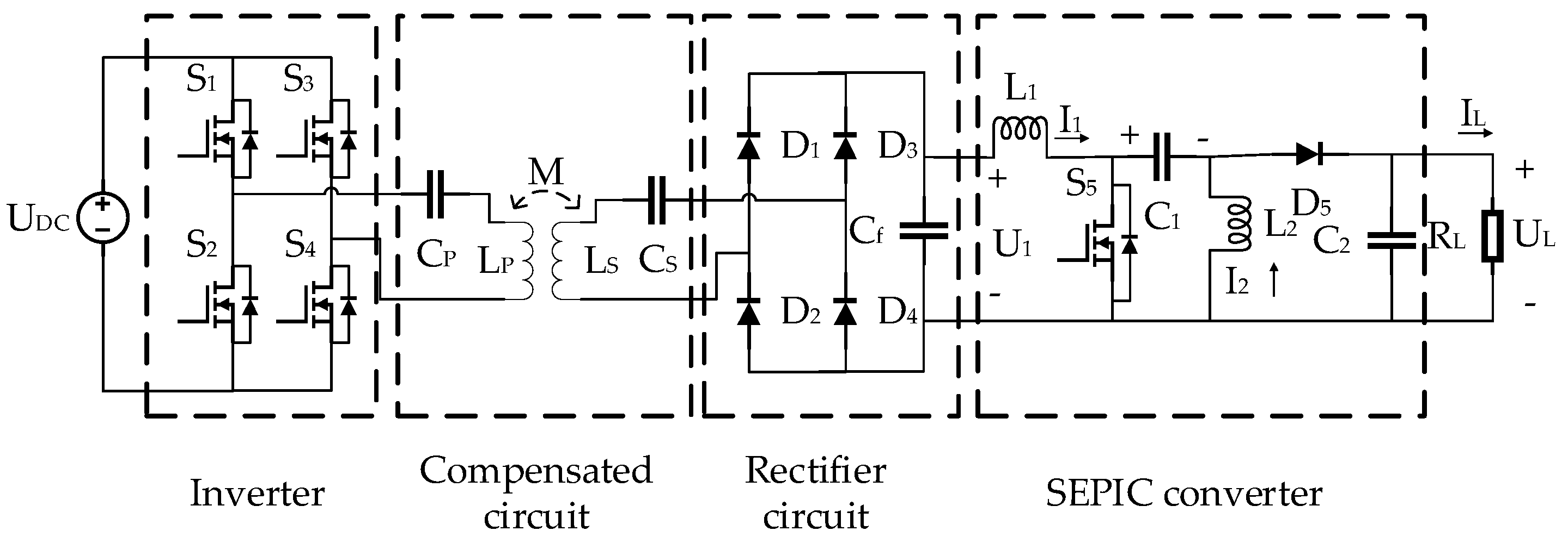
2. Proposed System
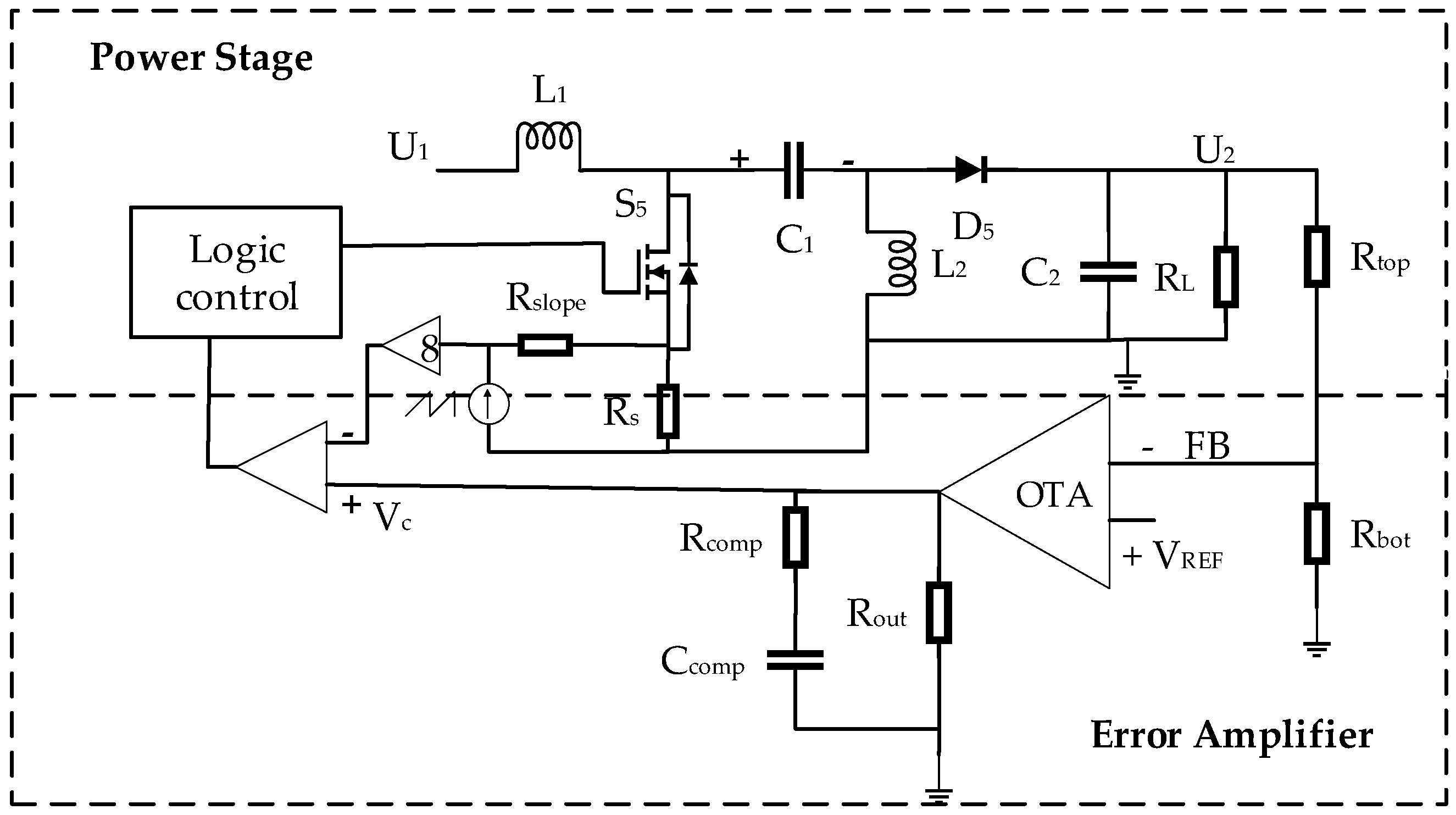
3. Circuit Design
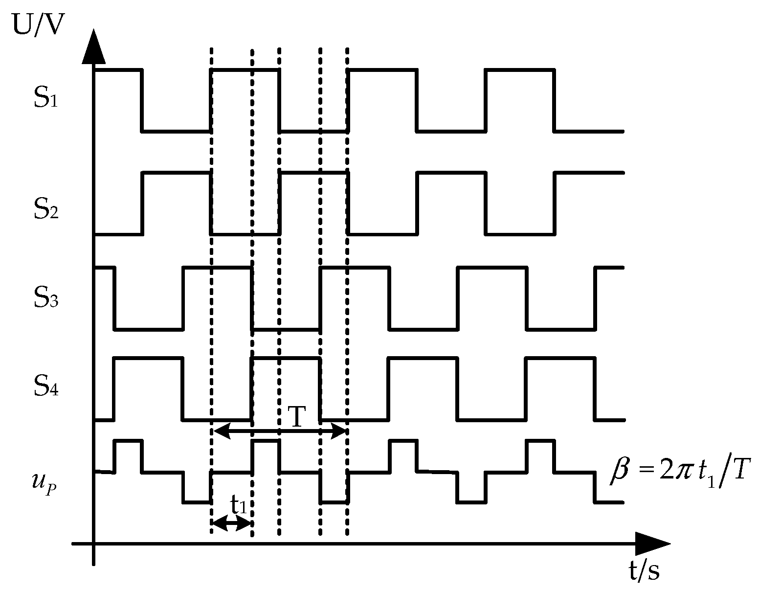
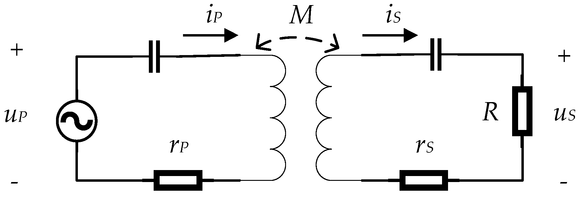
3.1. Primary Circuit Design
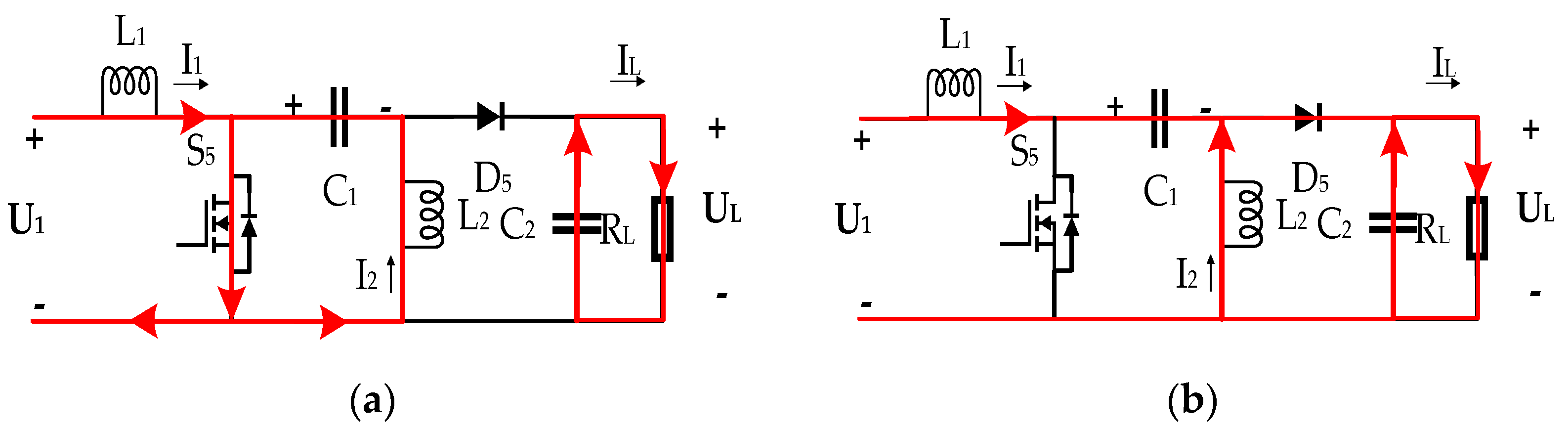
3.2. Secondary Circuit Design
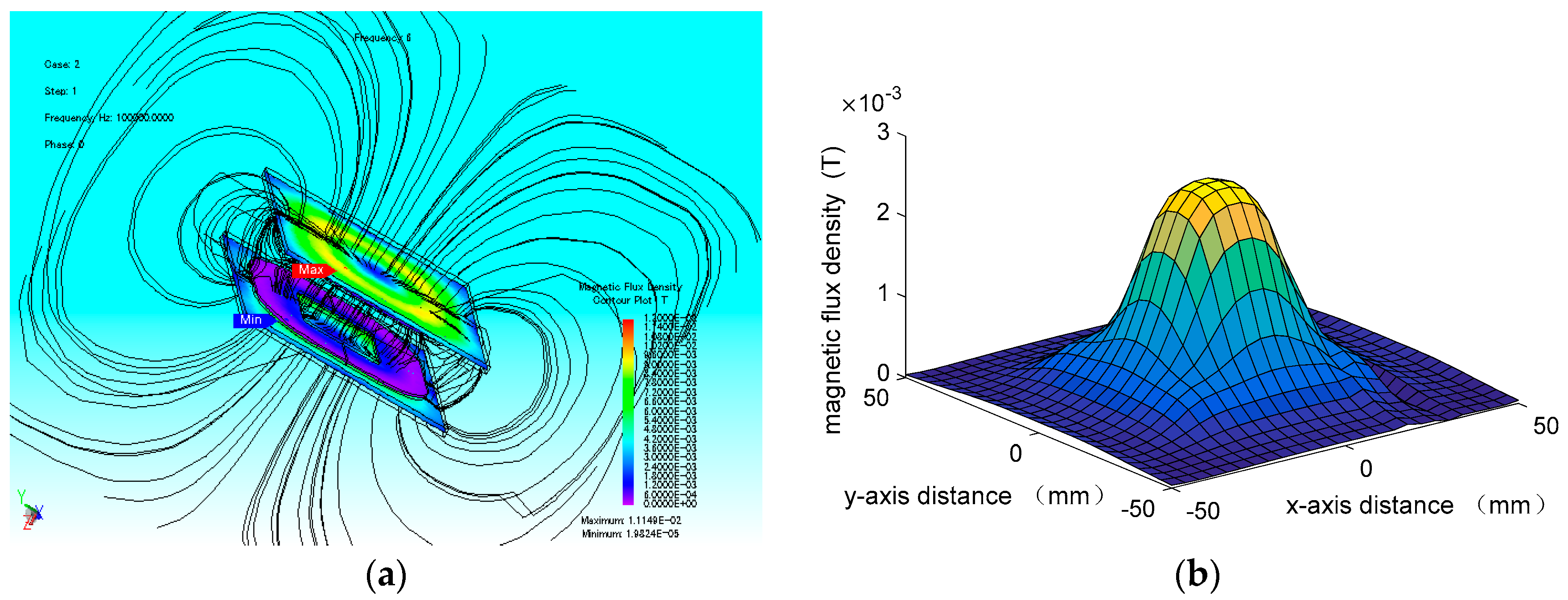
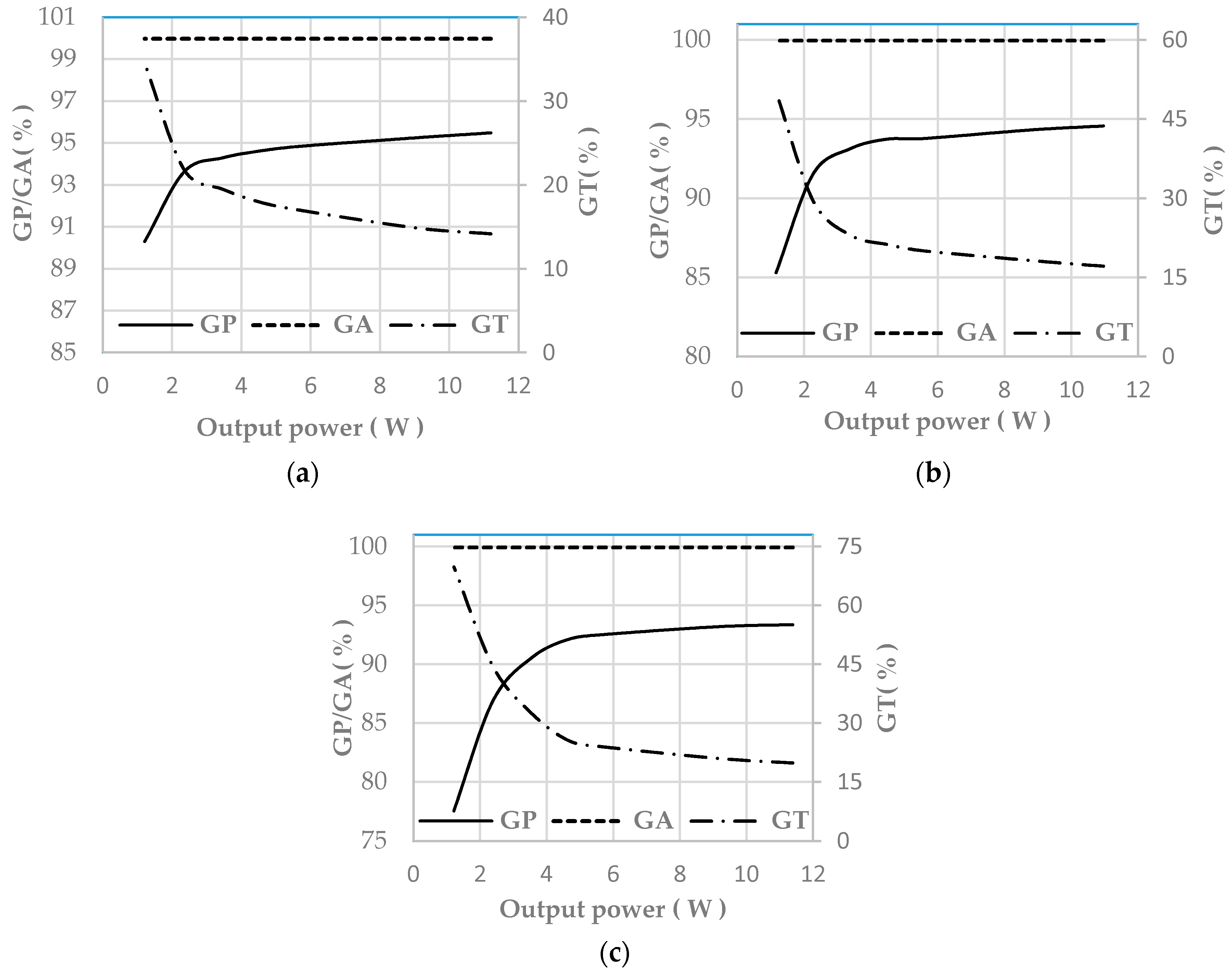
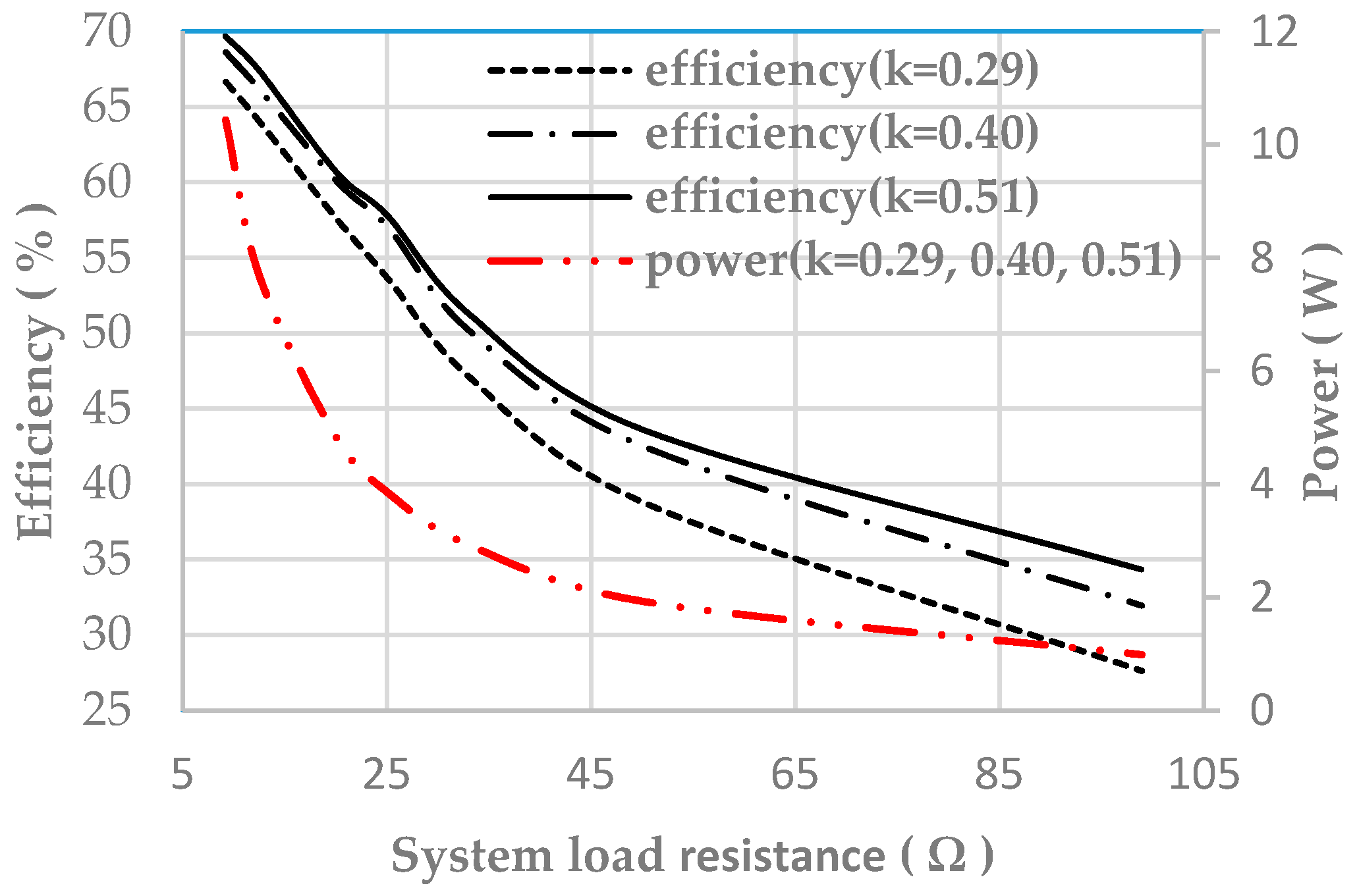
4. Simulation Results
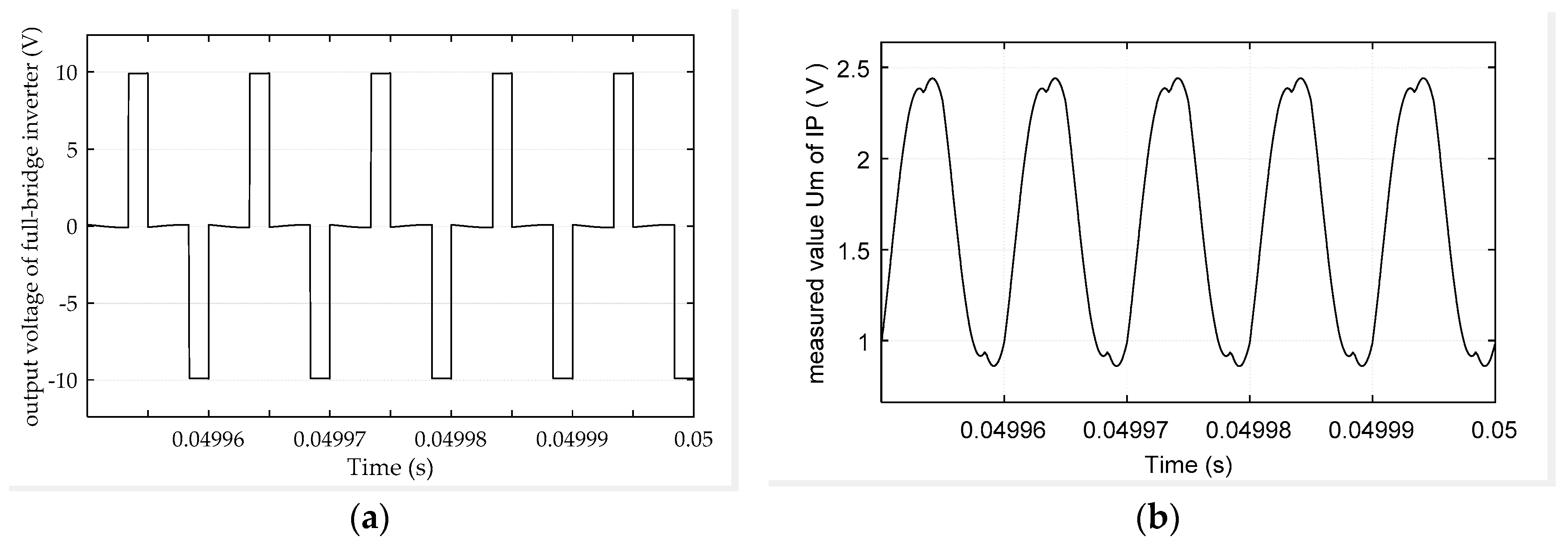
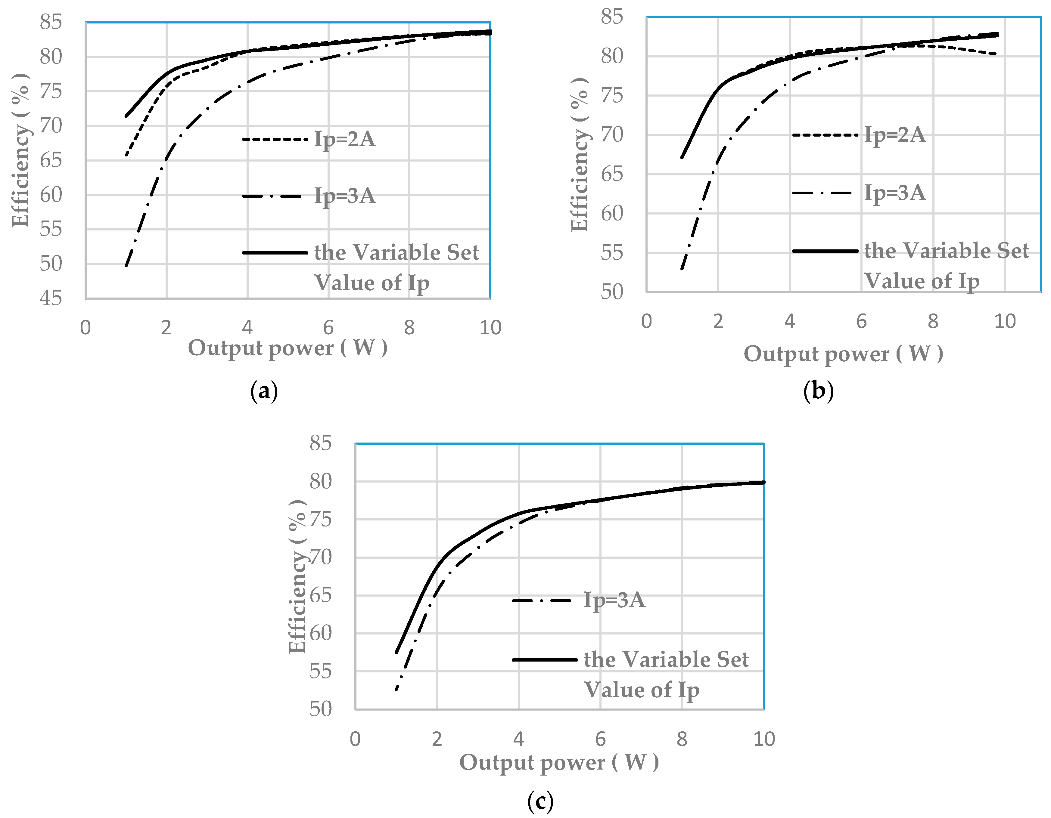
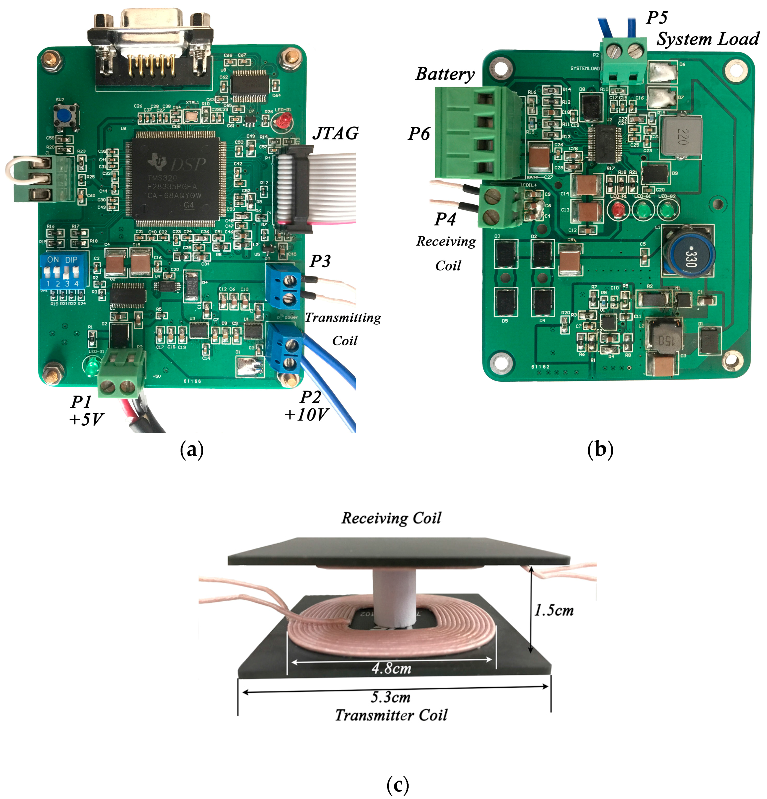
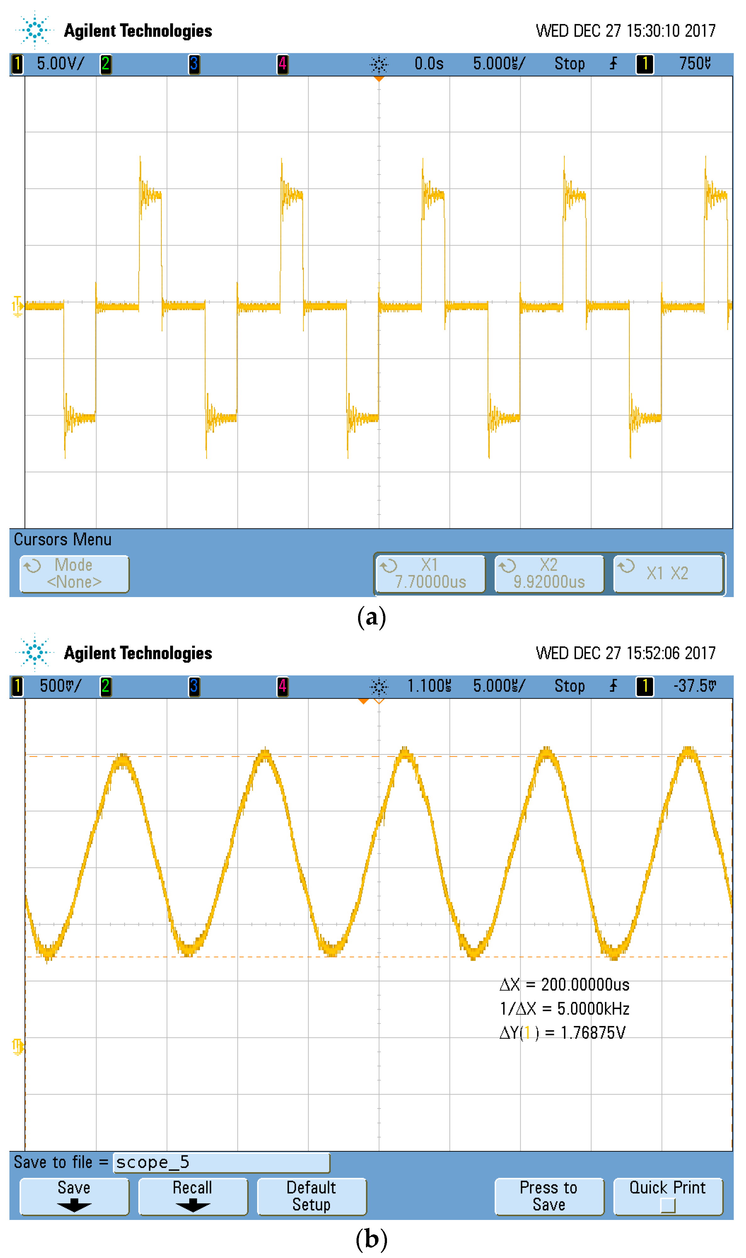
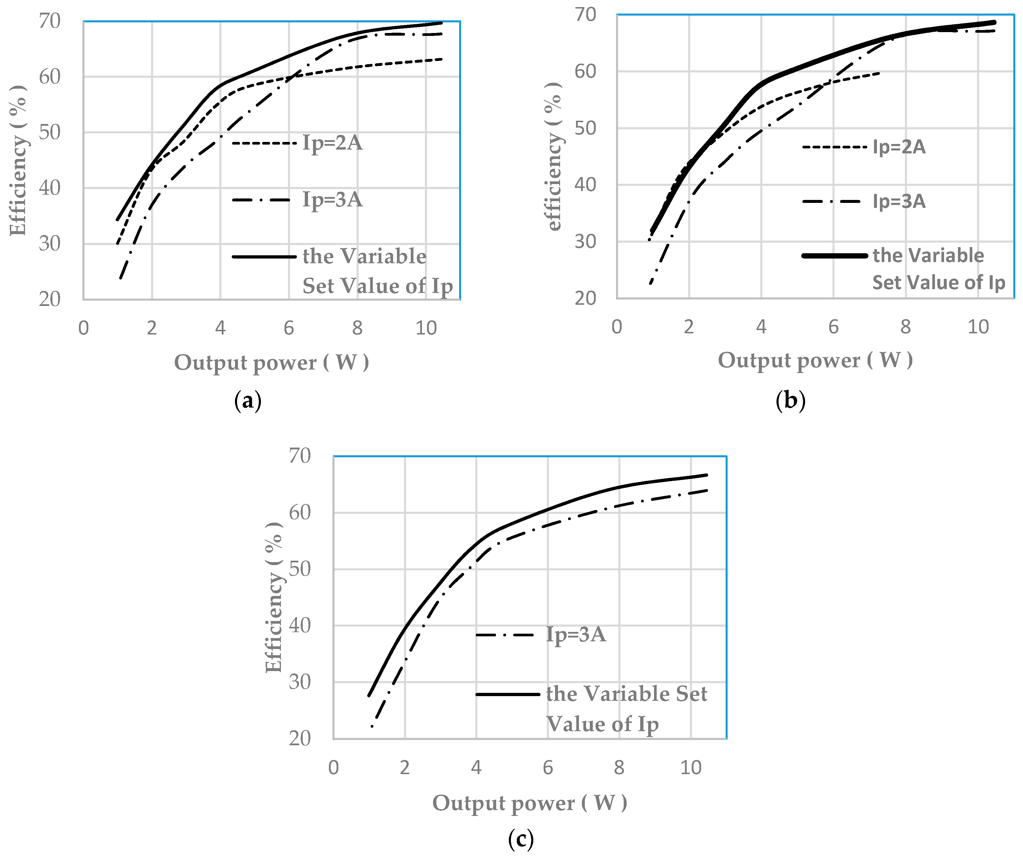
5. Experimental Results
6. Conclusions
Acknowledgments
Author Contributions
Conflicts of Interest
References
- Covic, G.A.; Boys, J.T. Inductive power transfer. Proc. IEEE 2013, 101, 1276–1289. [Google Scholar] [CrossRef]
- Jiang, C.; Chau, K.T.; Liu, C.; Lee, C.H.T. An overview of resonant circuits for wireless power transfer. Energies 2017, 10, 894. [Google Scholar] [CrossRef]
- Hui, S.Y. Planar wireless charging technology for portable electronic products and qi. Proc. IEEE 2013, 101, 1290–1301. [Google Scholar] [CrossRef]
- Silay, K.M.; Dondi, D.; Larcher, L.; Declercq, M.; Benini, L.; Leblebici, Y.; Dehollain, C. Load optimization of an inductive power link for remote powering of biomedical implants. In Proceedings of the 2009 IEEE International Symposium on Circuits and Systems, Taipei, Taiwan, 24–27 May 2009; pp. 533–536. [Google Scholar]
- Peng, S.; Liu, M.; Tang, Z.; Ma, C. Optimal design of megahertz wireless power transfer systems for biomedical implants. In Proceedings of the 2017 IEEE 26th International Symposium on Industrial Electronics (ISIE), Edinburgh, UK, 19–21 June 2017; pp. 805–810. [Google Scholar]
- Xue, R.; Cheng, K.; Je, M. High-efficiency wireless power transfer for biomedical implants by optimal resonant load transformation. IEEE Trans. Circuits Syst. I Regul. Pap. 2013, 60, 867–874. [Google Scholar] [CrossRef]
- Liu, N.; Habetler, T.G. Design of an on-board charger for universal inductive charging in electric vehicles. In Proceedings of the 2015 IEEE Energy Conversion Congress and Exposition (ECCE), Montreal, QC, Canada, 20–24 September 2015; pp. 4544–4549. [Google Scholar]
- Li, B.; Geng, Y.; Lin, F.; Yang, Z.; Igarashi, S. Design of constant voltage compensation topology applied to wpt system for electrical vehicles. In Proceedings of the 2016 IEEE Vehicle Power and Propulsion Conference (VPPC), Hangzhou, China, 17–20 October 2016; pp. 1–6. [Google Scholar]
- Hata, K.; Imura, T.; Hori, Y. Maximum efficiency control of wireless power transfer via magnetic resonant coupling considering dynamics of dc-dc converter for moving electric vehicles. In Proceedings of the 2015 IEEE Applied Power Electronics Conference and Exposition (APEC), Charlotte, NC, USA, 15–19 March 2015; pp. 3301–3306. [Google Scholar]
- Patil, D.; Sirico, M.; Gu, L.; Fahimi, B. Maximum efficiency tracking in wireless power transfer for battery charger: Phase shift and frequency control. In Proceedings of the 2016 IEEE Energy Conversion Congress and Exposition (ECCE), Milwaukee, WI, USA, 18–22 September 2016; pp. 1–8. [Google Scholar]
- Liu, X.; Clare, L.; Yuan, X.; Wang, C.; Liu, J. A design method for making an lcc compensation two-coil wireless power transfer system more energy efficient than an ss counterpart. Energies 2017, 10, 1346. [Google Scholar] [CrossRef]
- Geng, Y.; Li, B.; Yang, Z.; Lin, F.; Sun, H. A high efficiency charging strategy for a supercapacitor using a wireless power transfer system based on inductor/capacitor/capacitor (lcc) compensation topology. Energies 2017, 10, 135. [Google Scholar] [CrossRef]
- Wang, C.S.; Covic, G.A.; Stielau, O.H. Power transfer capability and bifurcation phenomena of loosely coupled inductive power transfer systems. IEEE Trans. Ind. Electron. 2004, 51, 148–157. [Google Scholar] [CrossRef]
- Li, H.; Li, J.; Wang, K.; Chen, W.; Yang, X. A maximum efficiency point tracking control scheme for wireless power transfer systems using magnetic resonant coupling. IEEE Trans. Power Electron. 2015, 30, 3998–4008. [Google Scholar] [CrossRef]
- Fu, M.; Ma, C.; Zhu, X. A cascaded boost–buck converter for high-efficiency wireless power transfer systems. IEEE Trans. Ind. Inform. 2014, 10, 1972–1980. [Google Scholar] [CrossRef]
- Fu, M.; Yin, H.; Zhu, X.; Ma, C. Analysis and tracking of optimal load in wireless power transfer systems. IEEE Trans. Power Electron. 2015, 30, 3952–3963. [Google Scholar] [CrossRef]
- Zhong, W.X.; Hui, S.Y.R. Maximum energy efficiency tracking for wireless power transfer systems. IEEE Trans. Power Electron. 2015, 30, 4025–4034. [Google Scholar] [CrossRef]
- Huang, Y.; Shinohara, N.; Mitani, T. Impedance matching in wireless power transfer. IEEE Trans. Microw. Theory Tech. 2017, 65, 582–590. [Google Scholar] [CrossRef]
- Debbou, M.; Colet, F. Interleaved dc/dc charger for wireless power tranfer. In Proceedings of the 2017 IEEE International Conference on Industrial Technology (ICIT), Toronto, ON, Canada, 22–25 March 2017; pp. 1555–1560. [Google Scholar]
- Kobayashi, D.; Imura, T.; Hori, Y. Real-time coupling coefficient estimation and maximum efficiency control on dynamic wireless power transfer using secondary dc-dc converter. In Proceedings of the IECON 2015—41st Annual Conference of the IEEE Industrial Electronics Society, Yokohama, Japan, 9–12 November 2015; pp. 4650–4655. [Google Scholar]
- Yang, Y.; Liu, F.; Chen, X. A maximum power point tracking control scheme for magnetically coupled resonant wireless power transfer system by cascading sepic converter at the receiving side. In Proceedings of the 2017 IEEE Applied Power Electronics Conference and Exposition (APEC), Tampa, FL, USA, 26–30 March 2017; pp. 3702–3707. [Google Scholar]
- Dai, X.; Li, Y.; Deng, P.; Tang, C. A maximum power transfer tracking method for wpt systems with coupling coefficient identification considering two-value problem. Energies 2017, 10, 1665. [Google Scholar] [CrossRef]


| Parameters of the Coupled Circuit | Value | Parameters of the Dc-Dc Circuit | Value |
|---|---|---|---|
| LP/LS(rs/rp) | 10 μH (0.05 Ω) | L1 | 33 μH |
| CP/CS | 0.247 μF | L2 | 15 μH |
| UDC | 10 V | C1 | 4.7 μF |
| POUT_max | 9.78 W | C2 | 22 μF |
| UL | 9.89 V | ||
© 2018 by the authors. Licensee MDPI, Basel, Switzerland. This article is an open access article distributed under the terms and conditions of the Creative Commons Attribution (CC BY) license (http://creativecommons.org/licenses/by/4.0/).
Share and Cite
Li, T.; Wang, X.; Zheng, S.; Liu, C. An Efficient Topology for Wireless Power Transfer over a Wide Range of Loading Conditions. Energies 2018, 11, 141. https://doi.org/10.3390/en11010141
Li T, Wang X, Zheng S, Liu C. An Efficient Topology for Wireless Power Transfer over a Wide Range of Loading Conditions. Energies. 2018; 11(1):141. https://doi.org/10.3390/en11010141
Chicago/Turabian StyleLi, Tianqing, Xiangzhou Wang, Shuhua Zheng, and Chunhua Liu. 2018. "An Efficient Topology for Wireless Power Transfer over a Wide Range of Loading Conditions" Energies 11, no. 1: 141. https://doi.org/10.3390/en11010141
APA StyleLi, T., Wang, X., Zheng, S., & Liu, C. (2018). An Efficient Topology for Wireless Power Transfer over a Wide Range of Loading Conditions. Energies, 11(1), 141. https://doi.org/10.3390/en11010141