
SHA-256 Hardware Proposal for IoT Devices in the Blockchain Context

 , , , and
Abstract
1. Introduction
- Enhanced processing capacity: By utilizing a multi-core architecture on the FPGA, the proposed implementation significantly improves the processing capacity of IoT devices, achieving a throughput of approximately 1.4 Gbps for 16 cores on a single FPGA.
- Energy efficiency: The FPGA implementation demonstrates substantial power savings, reducing dynamic power consumption by nearly 1000 times compared to existing solutions, making it suitable for power-constrained IoT applications.
- Security and privacy: Integrating the SHA-256 algorithm into IoT devices enhances data integrity and confidentiality, addressing critical security and privacy concerns in IoT communications.
- Scalability and flexibility: The FPGA-based approach provides a flexible and scalable solution that can be adapted to various IoT scenarios, including smart cities, the Industrial IoT, and real-time healthcare monitoring systems.
2. Related Work
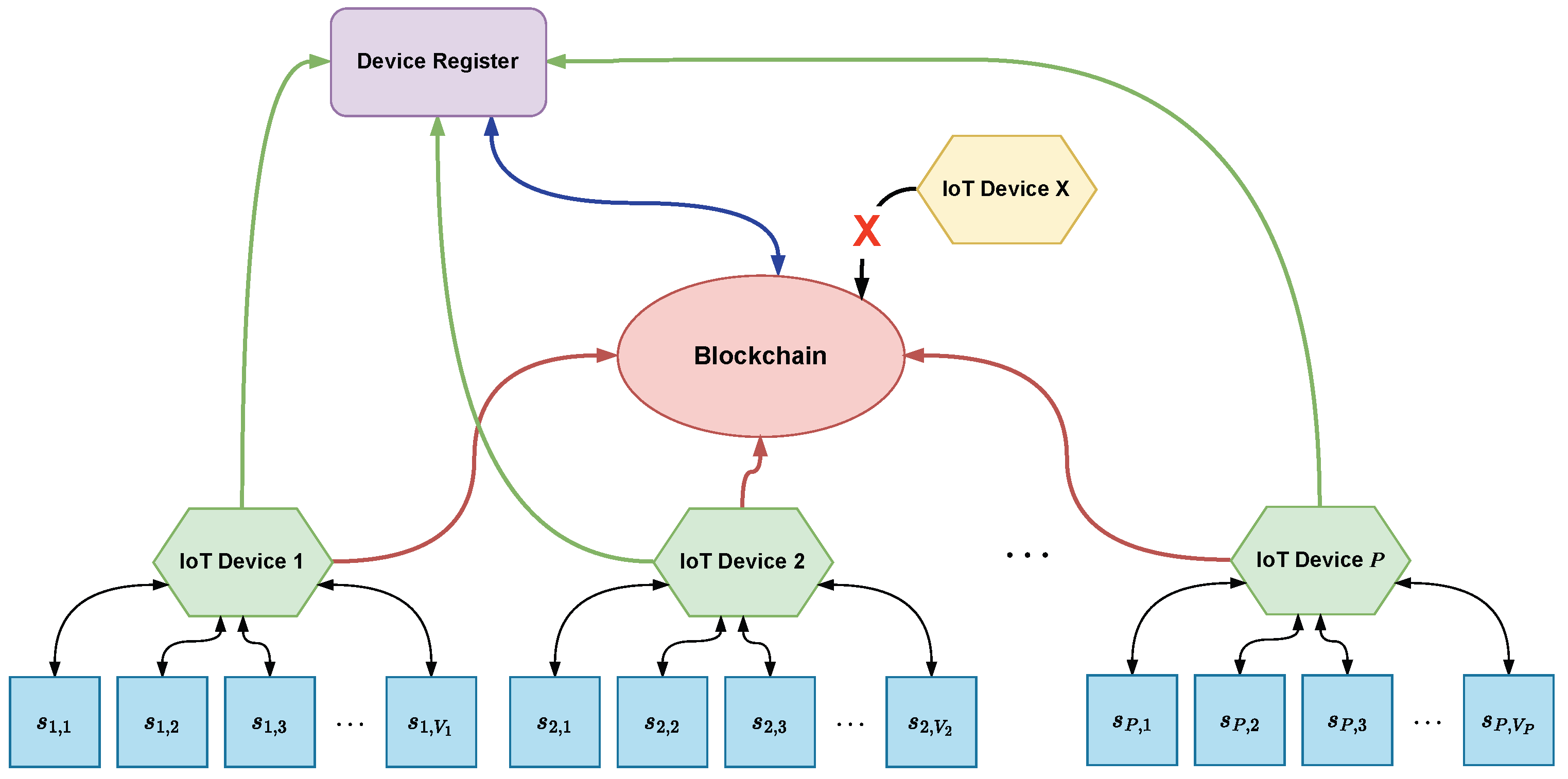
3. Blockchain in the IoT
3.1. Blockchain Overview
3.2. Blockchain in the IoT
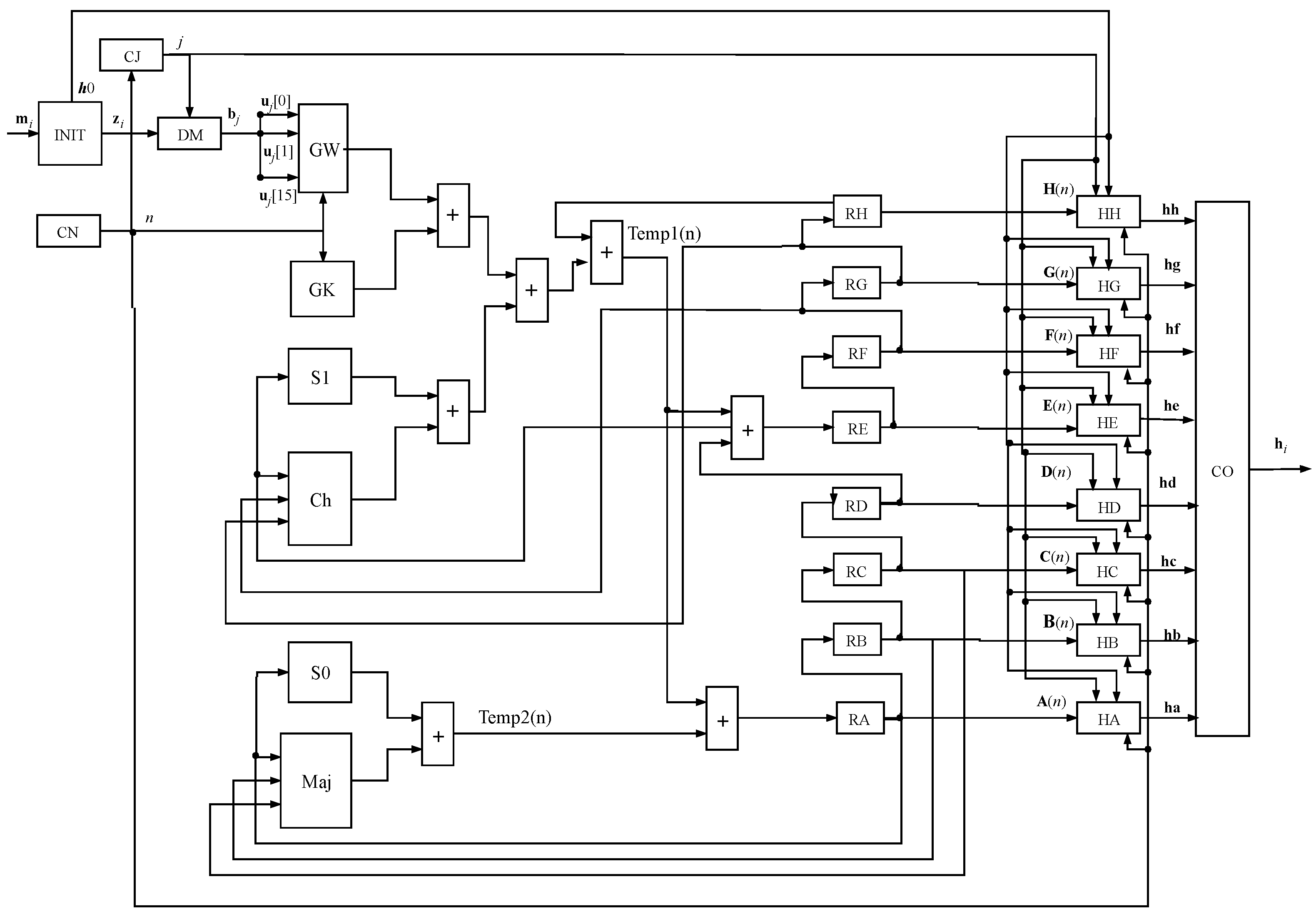
4. SHA-256 Algorithm Description
| Algorithm 1 SHA-256 for each i-th message |
|
5. SHA-256 Implementation on Reconfigurable Hardware
6. Analysis and Results
6.1. Hardware Validation
6.2. Power Consumption
6.3. Blockchain in the IoT with FPGA
7. Conclusions
Author Contributions
Funding
Data Availability Statement
Conflicts of Interest
References
- ISO/IEC JTC 1; Information Technology—Security Techniques—Code of Practice for Information Security Controls. Standard, International Organization for Standardization and International Electrotechnical Commission: Geneva, Switzerland, 2013.
- Martino, R.; Cilardo, A. SHA-2 Acceleration Meeting the Needs of Emerging Applications: A Comparative Survey. IEEE Access 2020, 8, 28415–28436. [Google Scholar] [CrossRef]
- Michail, H.E.; Athanasiou, G.S.; Kelefouras, V.; Theodoridis, G.; Goutis, C.E. On the Exploitation of a High-throughput SHA-256 FPGA Design for HMAC. ACM Trans. Reconfigurable Technol. Syst. 2012, 5, 1–28. [Google Scholar] [CrossRef]
- Asano, S.; Maruyama, T.; Yamaguchi, Y. Performance comparison of FPGA, GPU and CPU in image processing. In Proceedings of the 2009 International Conference on Field Programmable Logic and Applications, Sydney, Australia, 9–11 December 2009; pp. 126–131. [Google Scholar] [CrossRef]
- Kuon, I.; Rose, J. Measuring the Gap Between FPGAs and ASICs. IEEE Trans. Comput. Aided Des. Integr. Circuits Syst. 2007, 26, 203–215. [Google Scholar] [CrossRef]
- Da Silva, L.M.D.; Torquato, M.F.; Fernandes, M.A.C. Parallel Implementation of Reinforcement Learning Q-Learning Technique for FPGA. IEEE Access 2019, 7, 2782–2798. [Google Scholar] [CrossRef]
- Da Costa, A.L.X.; Silva, C.A.D.; Torquato, M.F.; Fernandes, M.A.C. Parallel Implementation of Particle Swarm Optimization on FPGA. IEEE Trans. Circuits Syst. II Express Briefs 2019, 66, 1875–1879. [Google Scholar] [CrossRef]
- Torquato, M.F.; Fernandes, M.A.C. High-Performance Parallel Implementation of Genetic Algorithm on FPGA. Circuits Syst. Signal Process. 2019, 38, 4014–4039. [Google Scholar] [CrossRef]
- Shi, Z.; Ma, C.; Cote, J.; Wang, B. Hardware implementation of hash functions. In Introduction to Hardware Security and Trust; Springer: Berlin/Heidelberg, Germany, 2012; pp. 27–50. [Google Scholar]
- Da Silva, L.M.D.; Coutinho, M.G.F.; Santos, C.E.B.; Santos, M.R.; Ruiz, M.D.; Guedes, L.A.; Fernandes, M.A.C. Hardware Architecture Proposal for TEDA Algorithm to Data Streaming Anomaly Detection. IEEE Access 2021, 9, 103141–103152. [Google Scholar] [CrossRef]
- Thomas, A.; Bhakthavatchalu, R. Implementation of SHA 256 using MATLAB and on FPGA by the Application of Block Chain Concepts. In Proceedings of the 2021 International Conference on Communication, Control and Information Sciences (ICCISc), Idukki, India, 16–18 June 2021; Volume 1, pp. 1–5. [Google Scholar]
- Devika, K.N.; Bhakthavatchalu, R. Parameterizable FPGA Implementation of SHA-256 using Blockchain Concept. In Proceedings of the 2019 International Conference on Communication and Signal Processing (ICCSP), Chennai, India, 4–6 April 2019; pp. 0370–0374. [Google Scholar] [CrossRef]
- Martino, R.; Cilardo, A. Designing a SHA-256 processor for blockchain-based IoT applications. Internet Things 2020, 11, 100254. [Google Scholar] [CrossRef]
- Abdelmaboud, A.; Ahmed, A.I.A.; Abaker, M.; Eisa, T.A.E.; Albasheer, H.; Ghorashi, S.A.; Karim, F.K. Blockchain for IoT applications: Taxonomy, platforms, recent advances, challenges and future research directions. Electronics 2022, 11, 630. [Google Scholar] [CrossRef]
- Mozumder, M.A.I.; Sheeraz, M.M.; Athar, A.; Aich, S.; Kim, H.C. Overview: Technology roadmap of the future trend of metaverse based on IoT, blockchain, AI technique, and medical domain metaverse activity. In Proceedings of the 2022 24th International Conference on Advanced Communication Technology (ICACT), Pyeongchang, Republic of Korea, 13–16 February 2022; pp. 256–261. [Google Scholar]
- Liang, W.; Ji, N. Privacy challenges of IoT-based blockchain: A systematic review. Clust. Comput. 2022, 25, 2203–2221. [Google Scholar] [CrossRef]
- Azbeg, K.; Ouchetto, O.; Andaloussi, S.J. BlockMedCare: A healthcare system based on IoT, Blockchain and IPFS for data management security. Egypt. Inform. J. 2022, 23, 329–343. [Google Scholar] [CrossRef]
- Gugueoth, V.; Safavat, S.; Shetty, S.; Rawat, D. A review of IoT security and privacy using decentralized blockchain techniques. Comput. Sci. Rev. 2023, 50, 100585. [Google Scholar] [CrossRef]
- Kharche, A.; Badholia, S.; Upadhyay, R.K. Implementation of blockchain technology in integrated IoT networks for constructing scalable ITS systems in India. Blockchain Res. Appl. 2024, 100188. [Google Scholar] [CrossRef]
- Stallings, W. Cryptography and Network Security: Principles and Practice, 7th ed.; Person: São Paulo, SP, Brazil, 2017. [Google Scholar]
- Li, L.; Lin, S.; Shen, S.; Wu, K.; Li, X.; Chen, Y. High-throughput and area-efficient fully-pipelined hashing cores using BRAM in FPGA. Microprocess. Microsyst. 2019, 67, 82–92. [Google Scholar] [CrossRef]
- Abed, S.; Jaffal, R.; Mohd, B.J. A review on blockchain and IoT integration from energy, security and hardware perspectives. Wirel. Pers. Commun. 2023, 129, 2079–2122. [Google Scholar] [CrossRef]
- Khan, M.; Hatami, M.; Zhao, W.; Chen, Y. A novel trusted hardware-based scalable security framework for IoT edge devices. Discov Internet Things 2024, 4, 4. [Google Scholar] [CrossRef]
- Ktari, J.; Frikha, T.; Hamdi, M.; Hamam, H. Enhancing Blockchain Consensus with FPGA: Accelerating Implementation for Efficiency. IEEE Access 2024, 12, 44773–44785. [Google Scholar] [CrossRef]
- Caraveo-Cacep, M.A.; Vázquez-Medina, R.; Hernández Zavala, A. A review on security implementations in soft-processors for IoT applications. Comput. Secur. 2024, 139, 103677. [Google Scholar] [CrossRef]
- Proulx, A.; Chouinard, J.Y.; Fortier, P.; Miled, A. A survey on fpga cybersecurity design strategies. ACM Trans. Reconfigurable Technol. Syst. 2023, 16, 1–33. [Google Scholar] [CrossRef]
- Bhuyan, M.; Kashihara, S.; Fall, D.; Taenaka, Y.; Kadobayashi, Y. A survey on blockchain, SDN and NFV for the smart-home security. Internet Things 2022, 20, 100588. [Google Scholar]
- Coppolino, L.; D’Antonio, S.; Mazzeo, G.; Romano, L. A comprehensive survey of hardware-assisted security: From the edge to the cloud. Internet Things 2019, 6, 100055. [Google Scholar] [CrossRef]
- El Jaouhari, S.; Bouvet, E. Secure firmware Over-The-Air updates for IoT: Survey, challenges, and discussions. Internet Things 2022, 18, 100508. [Google Scholar] [CrossRef]
- Ting, K.K.; Yuen, S.C.L.; Lee, K.H.; Leong, P.H.W. An FPGA Based SHA-256 Processor. In Field-Programmable Logic and Applications: Reconfigurable Computing Is Going Mainstream; Glesner, M., Zipf, P., Renovell, M., Eds.; Springer: Berlin/Heidelberg, Germany, 2002; pp. 577–585. [Google Scholar]
- Sklavos, N.; Koufopavlou, O. Implementation of the SHA-2 Hash Family Standard Using FPGAs. J. Supercomput. 2005, 31, 227–248. [Google Scholar] [CrossRef]
- García, R.; Algredo-Badillo, I.; Morales-Sandoval, M.; Feregrino-Uribe, C.; Cumplido, R. A compact FPGA-based processor for the Secure Hash Algorithm SHA-256. Comput. Electr. Eng. 2014, 40, 194–202. [Google Scholar] [CrossRef]
- Padhi, M.; Chaudhari, R. An optimized pipelined architecture of SHA-256 hash function. In Proceedings of the 2017 7th International Symposium on Embedded Computing and System Design (ISED), Durgapur, India, 18–20 December 2017; pp. 1–4. [Google Scholar] [CrossRef]
- binti Suhaili, S.; Watanabe, T. Design of high-throughput SHA-256 hash function based on FPGA. In Proceedings of the 2017 6th International Conference on Electrical Engineering and Informatics (ICEEI), Langkawi, Malaysia, 25–27 November 2017; pp. 1–6. [Google Scholar] [CrossRef]
- Kammoun, M.; Elleuchi, M.; Abid, M.; BenSaleh, M.S. FPGA-based implementation of the SHA-256 hash algorithm. In Proceedings of the 2020 IEEE International Conference on Design Test of Integrated Micro Nano-Systems (DTS), Hammamet, Tunisia, 7–10 June 2020; pp. 1–6. [Google Scholar] [CrossRef]
- Chen, Y.; Li, S. A High-Throughput Hardware Implementation of SHA-256 Algorithm. In Proceedings of the 2020 IEEE International Symposium on Circuits and Systems (ISCAS), Virtual, 10–21 October 2020; pp. 1–4. [Google Scholar] [CrossRef]
- Kammoun, M.; Elleuchi, M.; Abid, M.; Obeid, A.M. HW/SW Architecture Exploration for an Efficient Implementation of the Secure Hash Algorithm SHA-256. J. Commun. Softw. Syst. 2021, 17, 87–96. [Google Scholar] [CrossRef]
- Kieu-Do-Nguyen, B.; Hoang, T.T.; Pham, C.K.; Pham-Quoc, C. A Power-efficient Implementation of SHA-256 Hash Function for Embedded Applications. In Proceedings of the 2021 International Conference on Advanced Technologies for Communications (ATC), Hanoi, Vietnam, 20–22 October 2021; pp. 39–44. [Google Scholar] [CrossRef]
- Bensalem, H.; Blaquière, Y.; Savaria, Y. Acceleration of the Secure Hash Algorithm-256 (SHA-256) on an FPGA-CPU Cluster Using OpenCL. In Proceedings of the 2021 IEEE International Symposium on Circuits and Systems (ISCAS), Daegu, Republic of Korea, 22–28 May 2021; pp. 1–5. [Google Scholar] [CrossRef]
- Fotohi, R.; Shams Aliee, F. Securing communication between things using blockchain technology based on authentication and SHA-256 to improving scalability in large-scale IoT. Comput. Netw. 2021, 197, 108331. [Google Scholar] [CrossRef]
- Ángel Prada-Delgado, M.; Baturone, I.; Dittmann, G.; Jelitto, J.; Kind, A. PUF-derived IoT identities in a zero-knowledge protocol for blockchain. Internet Things 2020, 9, 100057. [Google Scholar] [CrossRef]
- Ferreira, C.M.S.; Garrocho, C.T.B.; Oliveira, R.A.R.; Silva, J.S.; Cavalcanti, C.F.M.d.C. IoT Registration and Authentication in Smart City Applications with Blockchain. Sensors 2021, 21, 1323. [Google Scholar] [CrossRef]
- Sharma, P.; Moparthi, N.R.; Namasudra, S.; Shanmuganathan, V.; Hsu, C.H. Blockchain-based IoT architecture to secure healthcare system using identity-based encryption. Expert Systems 2022, 39, e12915. [Google Scholar] [CrossRef]
- Bhalaji, N.; Abilashkumar, P.C.; Aboorva, S. A Blockchain Based Approach for Privacy Preservation in Healthcare IoT. In ICICCT 2019—System Reliability, Quality Control, Safety, Maintenance and Management; Gunjan, V.K., Garcia Diaz, V., Cardona, M., Solanki, V.K., Sunitha, K.V.N., Eds.; Springer: Singapore, 2020; pp. 465–473. [Google Scholar]
- Siddiqui, M.F.; Ali, F.; Javed, M.A.; Khan, M.B.; Saudagar, A.K.J.; Alkhathami, M.; Abul Hasanat, M.H. An FPGA-Based Performance Analysis of Hardware Caching Techniques for Blockchain Key-Value Database. Appl. Sci. 2023, 13, 4092. [Google Scholar] [CrossRef]
- Qian, K.; Liu, Y.; He, X.; Du, M.; Zhang, S.; Wang, K. HPCchain: A Consortium Blockchain System based on CPU-FPGA Hybrid PUF for Industrial Internet of Things. IEEE Trans. Ind. Inform. 2023, 19, 11205–11215. [Google Scholar] [CrossRef]
- Gupta, Y.; Shorey, R.; Kulkarni, D.; Tew, J. The applicability of blockchain in the Internet of Things. In Proceedings of the 2018 10th International Conference on Communication Systems & Networks (COMSNETS), Bengaluru, India, 3–7 January 2018; pp. 561–564. [Google Scholar] [CrossRef]
- Nakamoto, S. Bitcoin: A peer-to-peer electronic cash system. Available online: https://bitcoin.org/bitcoin.pdf (accessed on 10 May 2024).
- Antonopoulos, A.M. Mastering Bitcoin: Programming the Open Blockchain, 2nd ed.; O’Reilly: Sebastopol, CA, USA, 2017. [Google Scholar]
- Yu, M.; Sahraei, S.; Li, S.; Avestimehr, S.; Kannan, S.; Viswanath, P. Coded Merkle Tree: Solving Data Availability Attacks in Blockchains. In Financial Cryptography and Data Security; Bonneau, J., Heninger, N., Eds.; Springer International Publishing: Cham, Switzerland, 2020; pp. 114–134. [Google Scholar]
- Li, X.; Wei, L.; Wang, L.; Ma, Y.; Zhang, C.; Sohail, M. A blockchain-based privacy-preserving authentication system for ensuring multimedia content integrity. Int. J. Intell. Syst. 2022, 37, 3050–3071. [Google Scholar] [CrossRef]
- Kumar, A.; Sharma, S.; Goyal, N.; Singh, A.; Cheng, X.; Singh, P. Secure and energy-efficient smart building architecture with emerging technology IoT. Comput. Commun. 2021, 176, 207–217. [Google Scholar] [CrossRef]
- Bao, Z.; Shi, W.; He, D.; Choo, K.R. IoTChain: A Three-Tier Blockchain-based IoT Security Architecture. arXiv 2018, arXiv:1806.02008. [Google Scholar]
- NIST. Secure Hash Standard (SHS). Available online: http://nvlpubs.nist.gov/nistpubs/FIPS/NIST.FIPS.180-4.pdf (accessed on 10 May 2024).
- Eastlake, D., III; Hansen, T. US Secure Hash Algorithms (SHA and SHA-based HMAC and HKDF). RFC 6234, Internet Engineering Task Force (IETF), 2011. Available online: https://www.rfc-editor.org/rfc/rfc6234.html (accessed on 10 May 2024).
- Conte, B. Crypto-Algorithms. Available online: https://github.com/B-Con/crypto-algorithms/blob/master/sha256.c (accessed on 10 May 2024).
- Rote, M.D.; Vijendran, N.; Selvakumar, D. High performance SHA-2 core using the Round Pipelined Technique. In Proceedings of the 2015 IEEE International Conference on Electronics, Computing and Communication Technologies (CONECCT), Bangalore, India, 10–11 July 2015; pp. 1–6. [Google Scholar] [CrossRef]
- Wong, M.M.; Pudi, V.; Chattopadhyay, A. Lightweight and High Performance SHA-256 using Architectural Folding and 4-2 Adder Compressor. In Proceedings of the 2018 IFIP/IEEE International Conference on Very Large Scale Integration (VLSI-SoC), Verona, Italy, 8–10 October 2018; pp. 95–100. [Google Scholar]
- Silva, S.; Fernandes Lopes, F.; Valderrama, C.; Fernandes, M. Proposal of Takagi-Sugeno Fuzzy-PI Controller Hardware. Sensors 2020, 20, 1996. [Google Scholar] [CrossRef]
- McCool, M.; Reinders, J.; Robison, A. Structured Parallel Programming: Patterns for Efficient Computation; Elsevier Science: Amsterdam, The Netherlands, 2012. [Google Scholar]


| RN | PR | NLUT | PLUT | ||||
|---|---|---|---|---|---|---|---|
| (%) | (%) | (ns) | (Gbps) | (Watts) | |||
| 1 | 794 | 6730 | |||||
| 2 | 1582 | 13,482 | |||||
| 4 | 3158 | 26,933 | |||||
| 8 | 6313 | ||||||
| 16 | 12,618 | 107,609 |
| Reference | Speedup (Comparing This Work for Cores) | ||
|---|---|---|---|
| [30] 2002 | Virtex XCV300E−8 | ||
| [31] 2005 | Virtex | ||
| [3] 2012 | Xilinx | 11.008 | |
| [32] 2014 | Xilinx | ||
| [57] 2015 | Xilinx | ||
| [33] 2017 | Xilinx | ||
| [58] 2018 (Case I) | Xilinx | ||
| [58] 2018 (Case II) | Xilinx | ||
| [21] 2019 | Xilinx | ||
| [35] 2020 | Zynq−7000 | ||
| [36] 2020 | Xilinx | ||
| [37] 2021 | Zynq−7000 | ||
| [38] 2021 | Xilinx |
(MHz) | (Gbps) | (Mbps/Slice) | (Mbps/Slice/MHz) | |||
|---|---|---|---|---|---|---|
| [30] 2002 | Virtex | 1261 | 88 | |||
| [31] 2005 | Virtex | 2384 | 74 | |||
| [3] 2012 | Xilinx | 1831 | 172 | 11.008 | ||
| [32] 2014 | Xilinx | 139 | ||||
| [57] 2015 | Xilinx | 905 | 271 | |||
| [33] 2017 | Xilinx | 610 | ||||
| [58] | Xilinx | 382 | 238 | |||
| [58] | Xilinx | 485 | 222 | |||
| [21] 2019 | Xilinx | 11,660 | ||||
| [21] 2019—Adapted | Xilinx | 11,660 | ||||
| [35] 2020 | Zynq−7000 | 6367 | 181 | |||
| [36] 2020 | Xilinx | 979 | 255.7 | |||
| [37] 2021 | Zynq−7000 | 1305 | 135 | |||
| [38] 2021 | Zynq−7000 | 327 | 141.84 | |||
( core) | Xilinx | 1933 | ||||
( cores) | Xilinx | 28,830 |
| Reference | (MHz) | ||||||
|---|---|---|---|---|---|---|---|
| [30] 2002 | Virtex | 1261 | 88 | 218,83× | |||
| [31] 2005 | Virtex | 2384 | 74 | ||||
| [3] 2012 | Xilinx | 1831 | 172 | 11.008 | 2372.54× | ||
| [32] 2014 | Xilinx | 139 | |||||
| [57] 2015 | Xilinx | 905 | 271 | ||||
| [33] 2017 | Xilinx | 610 | |||||
| [58] 2018 (Case I) | Xilinx | 382 | 238 | ||||
| [58] 2018 (Case II) | Xilinx | 485 | 222 | ||||
| [21] 2019—Adapted | Xilinx | 11,660 | |||||
| [35] 2020 | Zynq−7000 | 6367 | 181 | ||||
| [36] 2020 | Xilinx | 979 | 255.7 | ||||
| [37] 2021 | Zynq−7000 | 1305 | 135 | ||||
| [38] 2021 | Xilinx | 327 | 141.84 | ||||
| This work () | Xilinx | 1993 | − | − | |||
| This work () | Xilinx | 12,618 | − | − |
| in Nano Sec (ns) | in s | ||
|---|---|---|---|
| 1 | 4 | ||
| 16 | 4 | ||
| 1 | 8 | ||
| 16 | 8 | ||
| 1 | 16 | ||
| 16 | 16 |
Disclaimer/Publisher’s Note: The statements, opinions and data contained in all publications are solely those of the individual author(s) and contributor(s) and not of MDPI and/or the editor(s). MDPI and/or the editor(s) disclaim responsibility for any injury to people or property resulting from any ideas, methods, instructions or products referred to in the content. |
© 2024 by the authors. Licensee MDPI, Basel, Switzerland. This article is an open access article distributed under the terms and conditions of the Creative Commons Attribution (CC BY) license (https://creativecommons.org/licenses/by/4.0/).
Share and Cite
Santos, C.E.B., Jr.; Silva, L.M.D.d.; Torquato, M.F.; Silva, S.N.; Fernandes, M.A.C. SHA-256 Hardware Proposal for IoT Devices in the Blockchain Context. Sensors 2024, 24, 3908. https://doi.org/10.3390/s24123908
Santos CEB Jr., Silva LMDd, Torquato MF, Silva SN, Fernandes MAC. SHA-256 Hardware Proposal for IoT Devices in the Blockchain Context. Sensors. 2024; 24(12):3908. https://doi.org/10.3390/s24123908
Chicago/Turabian StyleSantos, Carlos E. B., Jr., Lucileide M. D. da Silva, Matheus F. Torquato, Sérgio N. Silva, and Marcelo A. C. Fernandes. 2024. "SHA-256 Hardware Proposal for IoT Devices in the Blockchain Context" Sensors 24, no. 12: 3908. https://doi.org/10.3390/s24123908
APA StyleSantos, C. E. B., Jr., Silva, L. M. D. d., Torquato, M. F., Silva, S. N., & Fernandes, M. A. C. (2024). SHA-256 Hardware Proposal for IoT Devices in the Blockchain Context. Sensors, 24(12), 3908. https://doi.org/10.3390/s24123908