Abstract
One advantage of a resistive sensor array (RSA) with shared rows (M) and shared columns (N) is the reduced number of wires from M × N + 1 to M + N which can greatly lessen the complexity and burden on wearable electronic systems. However, the drawback is the crosstalk current effect between adjacent elements, which will lead to high measurement error. Although several solutions have been reported, they mainly focus on RSAs with high resistance (≥100 Ω). There is a lack of research that addresses RSAs with resistor values below 100 Ω. Here, we introduce a new circuit design named the dynamic zero current method (DZCM) to further decrease the measurement error. From the low value RSA test with ideal resistors, the DZCM exhibits lower error than the zero potential method (ZPM). In the case of the error variation ratio of amplifier offset voltage, the DZCM has a 4%/mV (row) to 7%/mV (column) ratio, while the ZPM has an almost 25%/mV (row) to 45%/mV (column) ratio and it increases with array size.
1. Introduction
Eutectic gallium indium (EGaIn), an alloy consisting of 75% gallium and 25% indium, is a low viscosity liquid metal at room temperature and has good electrical conductivity [1]. These unique characteristics of EGaIn make it an ideal active component to be embedded in soft sensors. Upon deformation of the sensor microstructure, which is pre-filled with EGaIn, the strain and pressure [2,3,4] exerted can be deduced easily from the measured varying capacitance and resistance.
By encapsulating EGaIn liquid metal with soft elastomers, our group has previously designed and fabricated EGaIn based microfluidic pressure sensors [5,6,7] with relatively low baseline resistance of 10 Ω (no load) which can go up to 200 Ω depending on the loading applied to it. Several examples employing such soft sensors have been demonstrated for healthcare and wearable electronics applications. Many of the current health sensing studies focus on the self-monitoring of personal health data. One such example is the tracking of plantar pressure of individuals with diabetes with diabetic foot ulcers via a flexible pressure sensitive insole embedded with soft sensors.
These sensors are stretchable, conformable and sensitive to mechanical loading and have great potential to be used as building blocks of electronic skins. Undoubtedly, a single sensor is not sufficient to replicate the function of human skin which has closely packed mechanoreceptors with very small receptive fields. To achieve high spatial resolution, a large number of small individual sensors are needed. These sensors are required to be merged firmly to form a compact resistive sensor array (RSA). An RSA enables a high density sensing element network to be configured with minimal wire linkage and thereby confers the least possible burden to the electrical system. One major concern of this RSA architecture is the crosstalk current effect resulting from adjacent unmeasured sensors that give rise to additional measurement error.
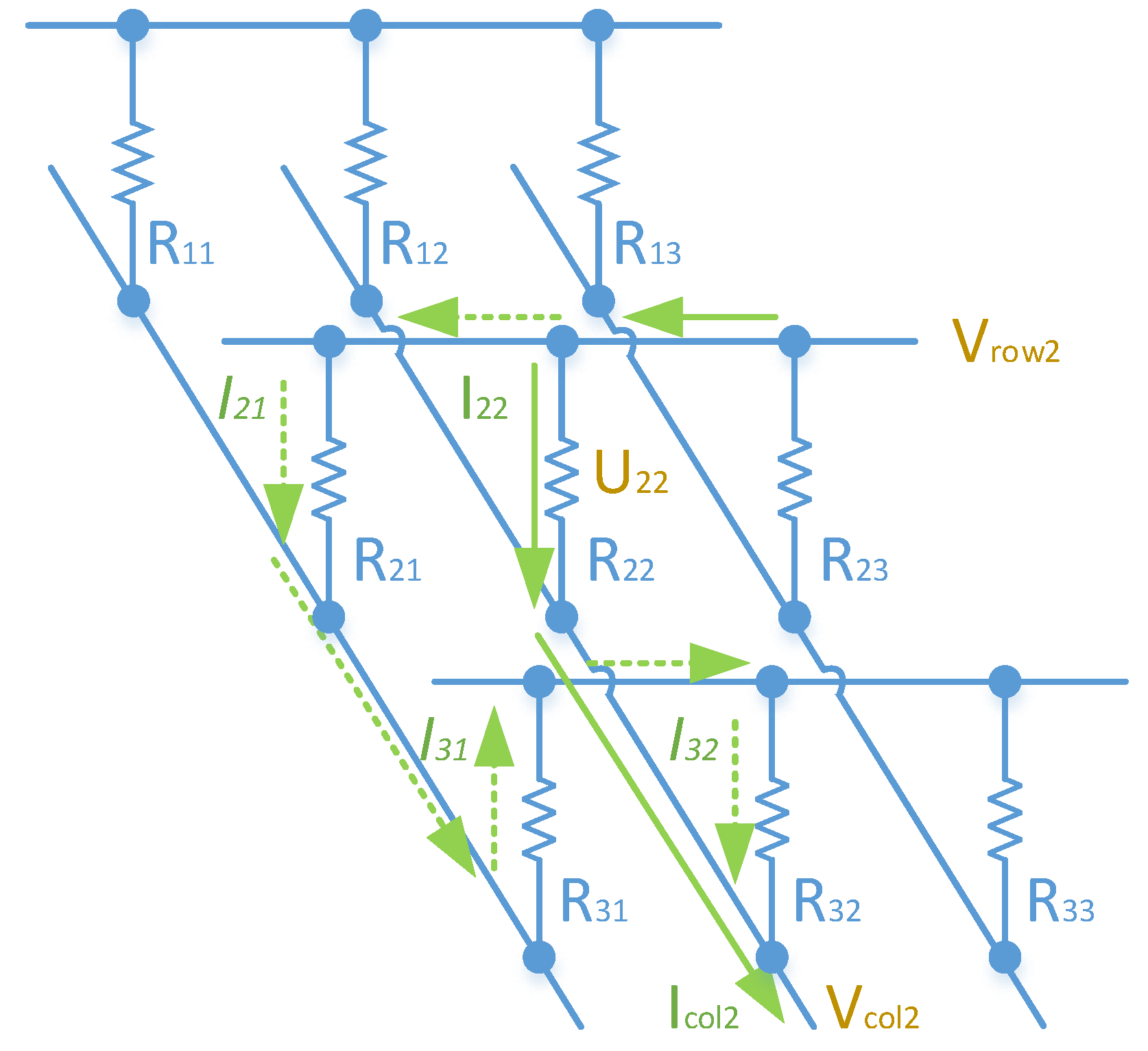
Figure 1 shows a 3 × 3 RSA. To calculate the resistance of the target resistor ‘R22′, we need to assess the current flowing through it and the voltage difference across the element, denoted as ‘I22′ and ‘U22′ accordingly. ‘U22′ also equals the voltage difference between the row and column wire ‘Vrow2–Vcol2′. On the other hand, ‘I22′ cannot be measured directly. ‘Icol2′ in the column wire is not equivalent to ‘I22′ as ‘Icol2′ includes crosstalk currents from the adjacent unmeasured resistors. The dashed arrow lines in Figure 1 illustrate one example of these crosstalk currents. Consequently, the actual value of ‘R22′ cannot be calculated easily from ‘Icol2′ and ‘U22′.
Figure 1.
Crosstalk currents induced in the resistor array.
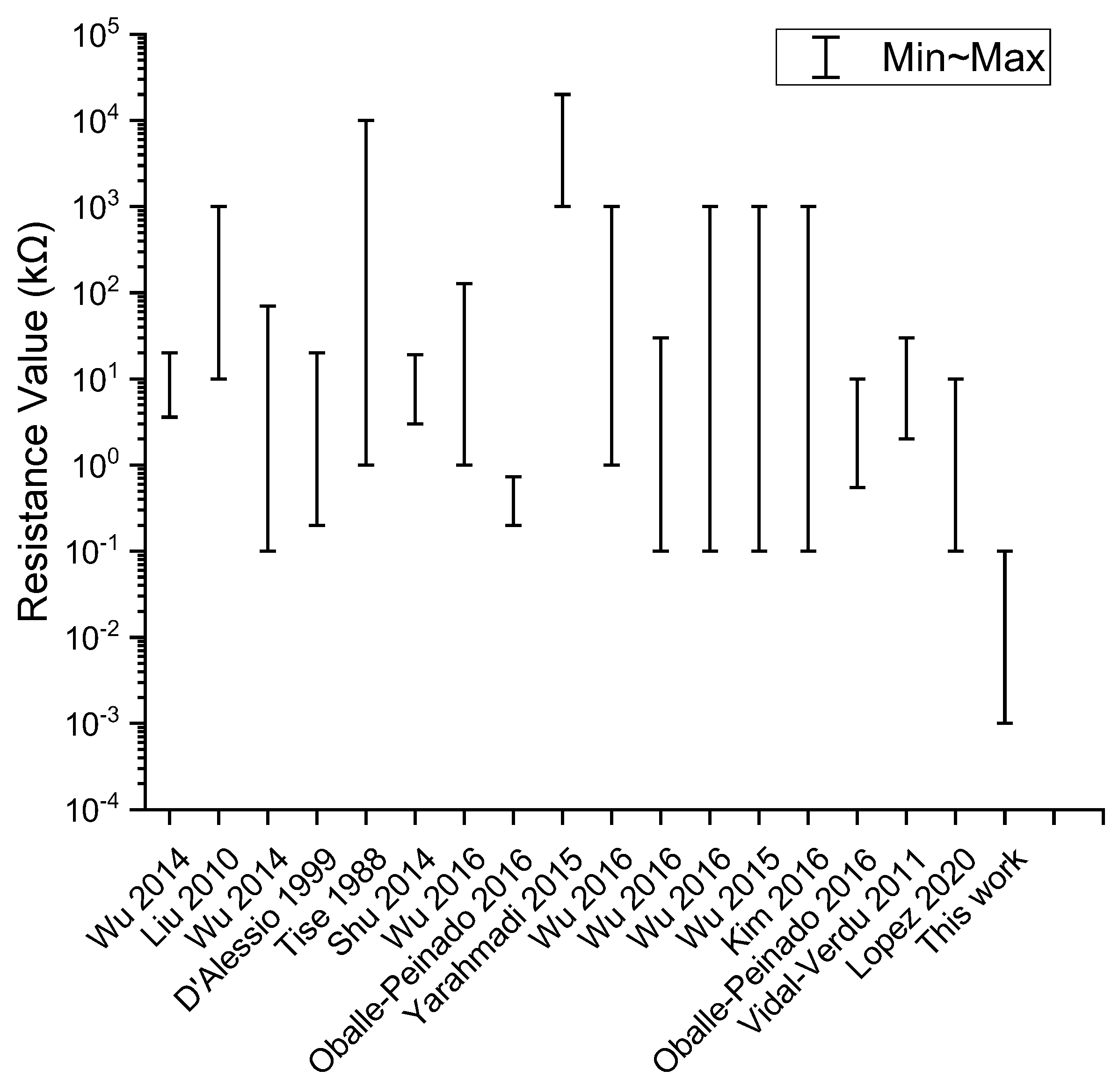
A number of RSA readout systems have been proposed to eliminate the crosstalk current effect. These approaches include the inserting diode method (IDM) [8,9], inserting transistor method (ITM) [10,11,12,13], passive integrator method (PIM) [14,15,16], resistance matrix approach (RMA) [17], improved RMA [18,19], incidence matrix approach (IMA) [20], voltage feedback method (VFM) [21,22,23,24,25,26,27,28,29,30] and zero potential method (ZPM) [29,31,32,33,34,35,36,37,38,39,40]. However, these systems only cater for RSA designs with high resistance. Electronic networks with low resistance below 100 Ω are often left unaddressed as shown in Figure 2.
Figure 2.
The range of resistance values addressed in different publications [14,15,16,17,19,21,24,25,27,28,29,30,33,34,36].
The lack in research progress on low resistance networks is partially attributed to the large crosstalk current effect and parasitic effect in the printed circuit board (PCB). In addition, the majority of the mechanical sensors and actuators in the market use high resistance transducers, due to the construction materials, fabrication techniques and sensing mechanisms involved.
Several methods, including the ZPM, VFM and IDM, have been developed to alleviate the crosstalk current effect. Based on a detailed comparative analysis [24], Liu concluded that the ZPM has the best performance, compared to the VFM and IDM. A detailed description of the ZPM is in Appendix A.
2. Dynamical Zero Current Method
In the discussion in Appendix A, we point out that the ZPM suffers from parasitic effects. The crosstalk current effect is deteriorated due to two reasons:
- Parasitic resistance from connection wires and PCB wires contributes a large crosstalk current effect.
- Offset voltage of row and column driving amplifiers induces a crosstalk current effect.
These two issues are difficult to eradicate, as they are caused by the intrinsic feature of these electrical components.
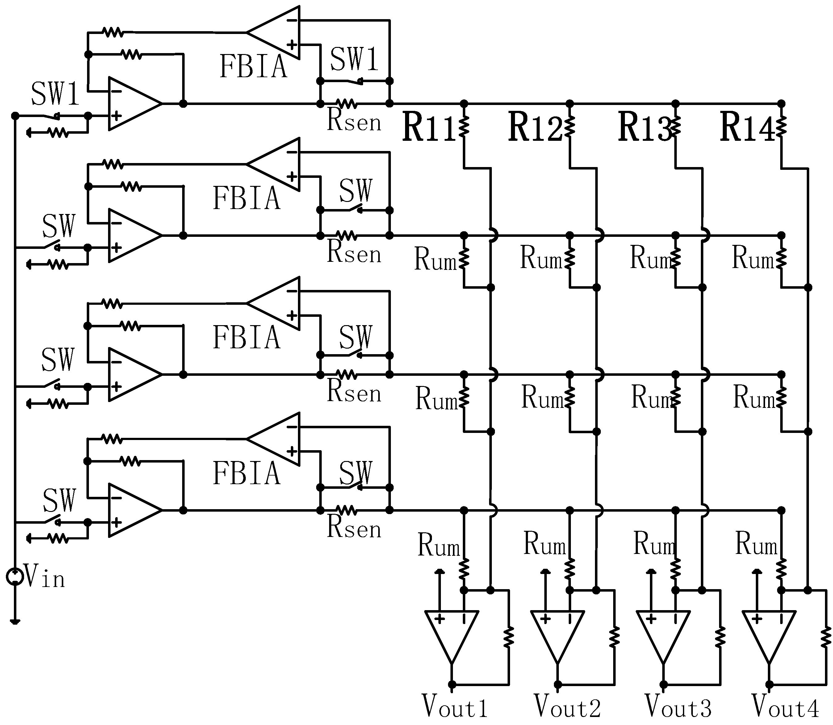
To fix the abovementioned problems, we proposed the DZCM. The DZCM is originated from the ZPM which drives both ends of the adjacent unmeasured resistors to zero potential. Thus, almost no current flows through these adjacent unmeasured resistors. Then, the crosstalk current path will be cut off. In the ZPM, because of the row/column parasitic resistance and row/column amplifier offset voltage, the zero current is not really zero. This amount of current is negligible in a large value RSA, but not so in the case of a low value RSA. This non-zero current must be minimized to reduce the measurement error in the low value RSAs. Based on the fundamental circuit topology of the ZPM, the proposed DZCM includes a feedback network to automatically enforce zero current through each row of the adjacent unmeasured resistors. This feedback feature is also able to flexibly adjust the node potential of the array resistors to match the varying row/column parasitic resistance and amplifier offset voltage in the readout system.
The DZCM circuit design for a 4 × 4 array is shown in Figure 3. is the current sensing resistor, which converts current to voltage. A feedback instrument amplifier (FBIA) magnifies the voltage across . SW1 are the switches with a closed (ON) state for rows containing measuring resistors and SW are the switches with an open (OFF) state for the adjacent unmeasured rows. All amplifiers in Figure 3 are non-ideal.
Figure 3.
The circuit design of DZCM for a 4 × 4 array.
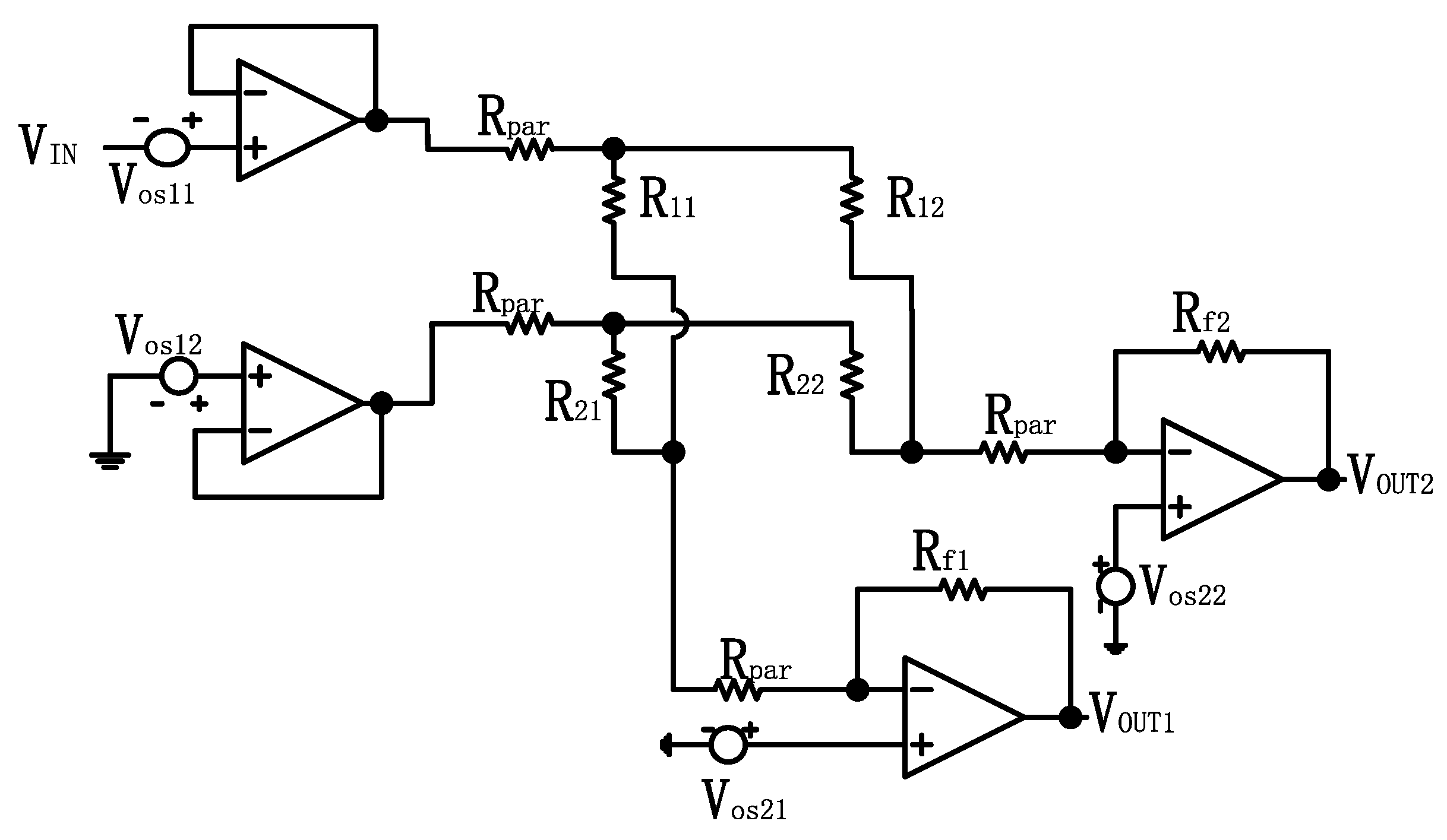
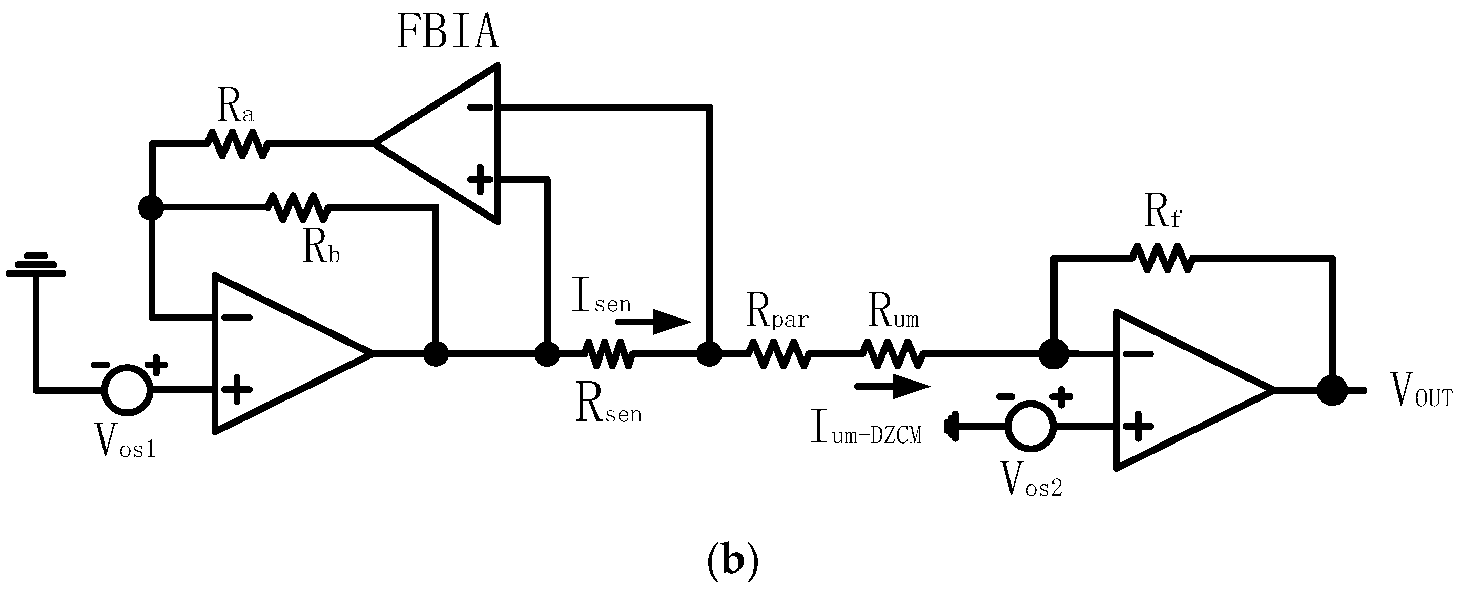
To explain the characteristics of the ZPM and DZCM more clearly, we simplify the network to just one unmeasured resistor to demonstrate the parasitic effect of this single resistor. Figure 4 shows the circuit of this simplified models, all amplifiers in Figure 4 are ideal.

Figure 4.
Simplification network with one unmeasured resistor of (a) ZPM and (b) DZCM.
We can derive the current of as:
and are the currents of the unmeasured resistor for the ZPM and DZCM, respectively. They are expressed in Equations (1a) and (1b) accordingly. and are the offset voltages of row and column driving amplifiers, is the parasitic resistance of row and column wires, is the resistance of the current sensing resistor, is the gain of FBIA r and is the current of sensing resistor.
From Equation (1a) for the ZPM and Equation (1a,b) for the DZCM, we can clearly see that computed from Equation (1b) is smaller than in Equation (1a) due to the presence of the term in the denominator.
We assume , , , , and . We can then easily evaluate and from Equation (1). is based on Equation (1a) for the ZPM and is based on Equation (1b) for the DZCM. Resulting from , and , the negative feedback in the DZCM decreases its parasitic effect current down to 1% of the parasitic effect current in the ZPM circuit. To put it simply, the DZCM can greatly minimize the measurement error in the low value RSA.
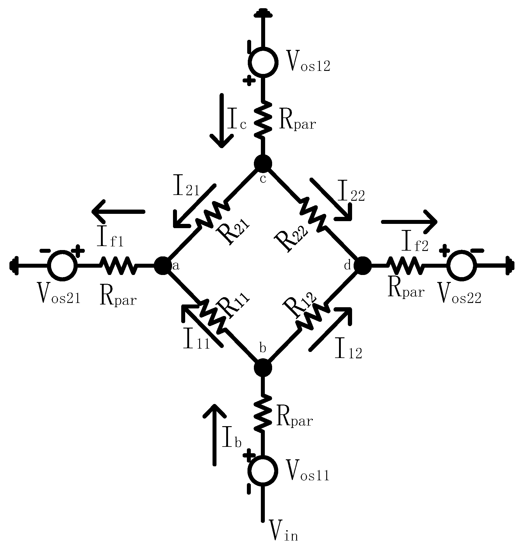
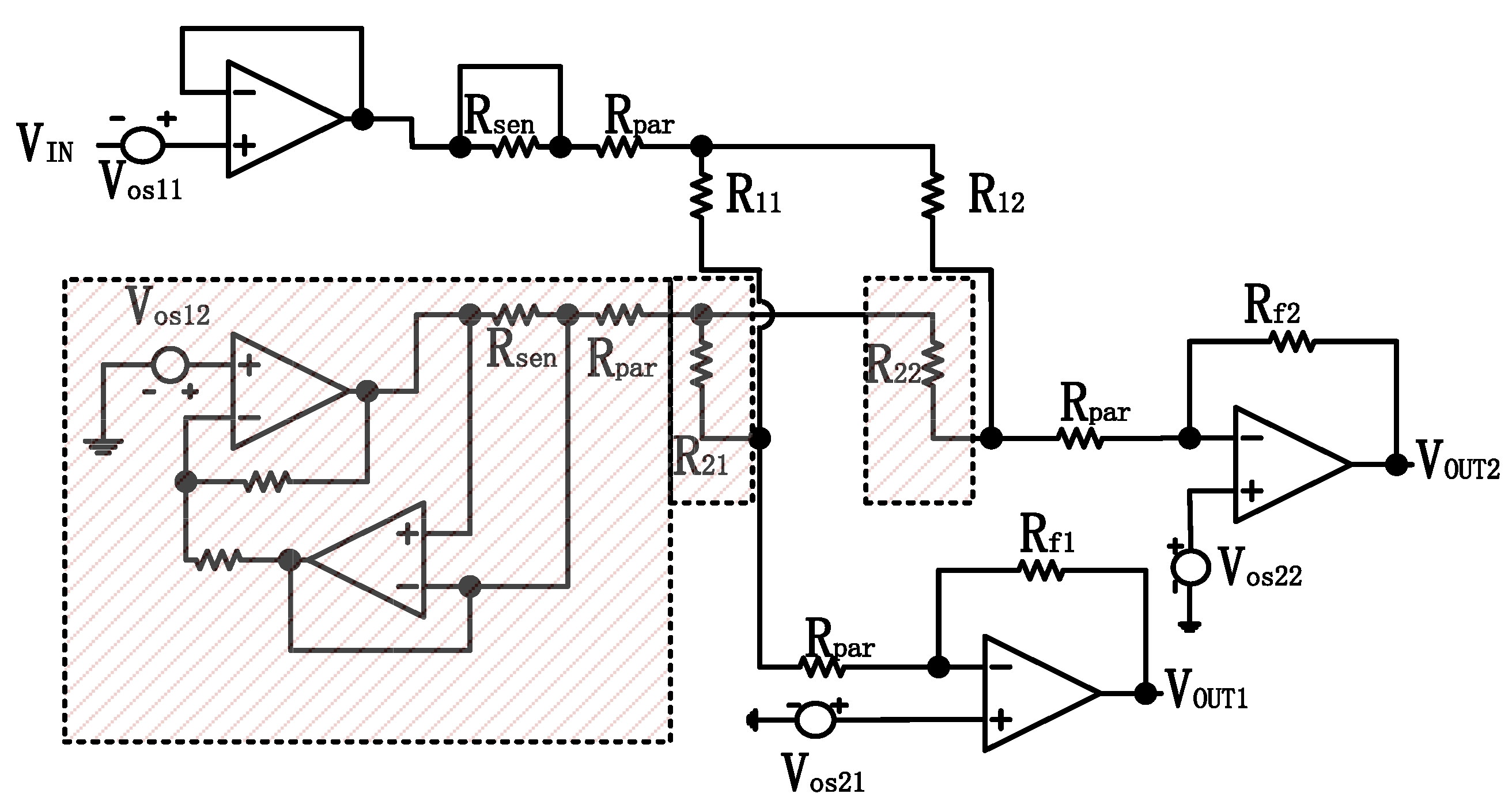
We further simplify the 4 × 4 array to a 2 × 2 array to quantify the crosstalk current effect in the DZCM, as shown in Figure 5. The reduced array network also includes a parasitic effect originated from , and . Based on the above discussion and Equation (1a) and Equation (1b), the currents of the adjacent unmeasured resistors and in the DZCM are only 1% of those in the ZPM. Thus, in the DZCM, the crosstalk current effect from and is minimal and negligible. Compared with Figure A3, and are shaded in Figure 5 and can be ignored in the Equation (2) formula derivation. The circuit diagram of Kirchhoff’s law, as shown in Figure 6, is used to analyze the DZCM network from Figure 5.
Figure 5.
A 2 × 2 array circuit model including parasitic effects and crosstalk current effect for DZCM.
Figure 6.
DZCM array network extracted and analyzed with Kirchhoff’s law.
In order to simplify calculation, we hypothesize that , and . After substituting (2a, 2b, 2c) with (2d, 2e), we obtain Equation (3).
Equation (3) is a non-homogeneous linear equation and after several solving steps in Appendix B, we have:
As , we can simplify Equation (4) as:
If we assume , Equation (A8) can be written as Equation (6):
It is clear to see the Equation (5) is similar to Equation (6), but Equation (5) does not have the term , which exists in Equation (6). This makes Equation (5) have a lower error resulting from .
3. Experiments for DZCM/ZPM and Discussion
Various experiments have been designed to evaluate the performances of the ZPM and DZCM under optimum circumstances. The experimental setup is shown in Table 1.
Table 1.
Experiments setup for DZCM with selected combinations.
The measurement result from a multimeter of an ideal single resistor is represented as . Meanwhile, the output amplifier’s voltage of array resistors is measured as by a multimeter. Using Equation (A1), we can obtain the resistance value of the resistor of interest, . The measurement percentage error between them is evaluated as follows:
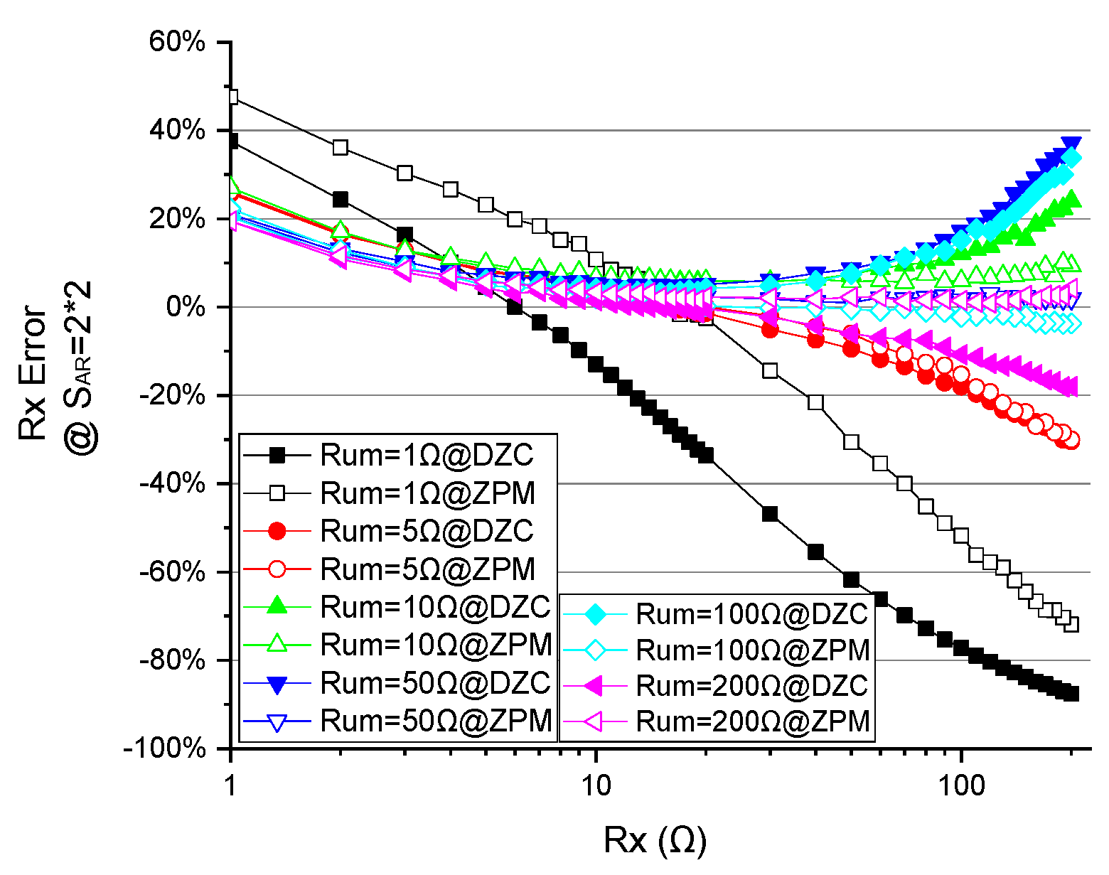
Experiment (EXP) A analyzes the effect of on in arrays of various sizes when the unmeasured array resistors are fixed at their lower and upper limits (i.e., 1 Ω and 200 Ω, respectively) and and are set to zero.
EXP B analyzes the effect of unmeasured array resistors on in the simplest 2 × 2 array, as increases and and are zero.
EXP C analyzes the effect of parasitic resistance of column and row ( and ) on when the unmeasured array resistors and are fixed at (), 50 Ω (), 200 Ω () and offset voltage is zero. The reason for increasing with increasing and is to avoid the crosstalk current effect, which will surpass the signal current of if is fixed to 10 mV and increases to 50 Ω or 200 Ω. The array size is set to 6 × 6 and 12 × 12.
EXP D analyzes the effect of on when the unmeasured array resistors and are fixed at 1 Ω (), 50 Ω (), 200 Ω () and is set to zero. The array size is set to 6 × 6 and 12 × 12.
3.1. Experimental Result for DZCM with Ideal Resistors
EXP A:
As shown in Figure 7a, with ,
Figure 7.
The effect of on measurement error of different when (a) and (b) in DZCM and ZPM (EXP A).
- i.
- the measurement errors of the DZCM and ZPM are found to be comparable when falls within the range of to . There is no significant improvement on the system performance by the additional feedback network of the DZCM in this range.
- ii.
- As goes beyond to , the e% of the DZCM is noticeably larger than that of the ZPM in all array sizes due to the underlying crosstalk current effect. The crosstalk current in the DZCM feedback network amounts to 25 µA, while the offset voltage of the feedback amplifier ‘AD623′ is 25 µV and the resistance value of the sensing resistor is 1 Ω. This gives rise to an undesired crosstalk current in , as, if and , we will have . Meanwhile, the offset voltage of the ZPM is intentionally and manually compensated to zero to minimize the crosstalk current down to zero. We used an adjustable resistor to form a reference voltage divider and connect it to the positive node of row/column amplifiers, shown as and , as displayed in Figure 4a. The result shows that the ZPM outperforms the DZCM within this range of , i.e., to , with notably smaller measurement error. Nonetheless, this crosstalk current effect in the DZCM can be further suppressed by increasing or in the feedback network.
In the case of (Figure 7b),
- i.
- e% of the DZCM is smaller than that of the ZPM within the range of to , showing the advantage of the DZCM feedback network in bringing down the crosstalk current.
- ii.
- As increases from to , measurement error changes from zero to a significant negative value. This unfavorable event also occurs in ZPM circuitry. Moreover, this event occurred in reference [29] Figure 4, Figure 5, Figure 6 and Figure 7 reference [39] Figure 8, reference [21] Figure 9, reference [36] Figure 5, reference [34] Figure 5, reference [30] Figure 9. We name this event the singular values effect (SVE), as it occurs when the measured resistor is tremendously different from the adjacent unmeasured resistors.
Figure 8. Simplified 2 × 2 array circuit example to demonstrate singular values effect in DZCM.
Figure 9. The effect of on measurement error of different when in DZCM and ZPM (EXP B).
A simple 2 × 2 array (see Figure 8) is illustrated to explain the SVE. Based on Figure 8, in the extreme case of , current flowing through decreases, denoted by . Meanwhile, for the adjacent resistor on the same row, . The current through , represented by , is equivalent to . Our measurement shows that the parasitic resistances resulting from the cable linking the sensor to PCB are and the voltage at column 2 is , and the voltage at column 1 is . Due to this potential difference between and , there will be a crosstalk current through and , . As are in the same order as , the measurement error can add up to 100%.
Figure 7 also shows the improvement of the DZCM in reducing measurement error in the range of and . That is to say, in low resistance RSA, the DZCM is capable of decreasing the measurement error.
EXP B:
As shown in Figure 9, the e% of the DZCM is smaller or similar to the ZPM in the range of . This measurement error in the DZCM becomes larger than the ZPM as increases to the range of , the increment has been explained in EXP A above as SVE.
EXP C:
As shown in Figure 10a,c,e, when (the parasitic resistor of row wires) changes from to and , the error of the ZPM is the same as in the DZCM.
Figure 10.
The effect of on measurement error of different when . (a,c,e) Effect of and (b,d,f) effect of in DZCM and ZPM (EXP C).
When (the parasitic resistor of column wires) changes from to , , as demonstrated in Figure 10b,d,f, the error of the ZPM is higher than that of the DZCM. The larger array size results in a greater error difference between the ZPM and DZCM. This error difference increases as goes up. This is due to the presence of the negative feedback network in the DZCM that effectively reduces the parasitic effect of in the low resistance domain.
EXP D:
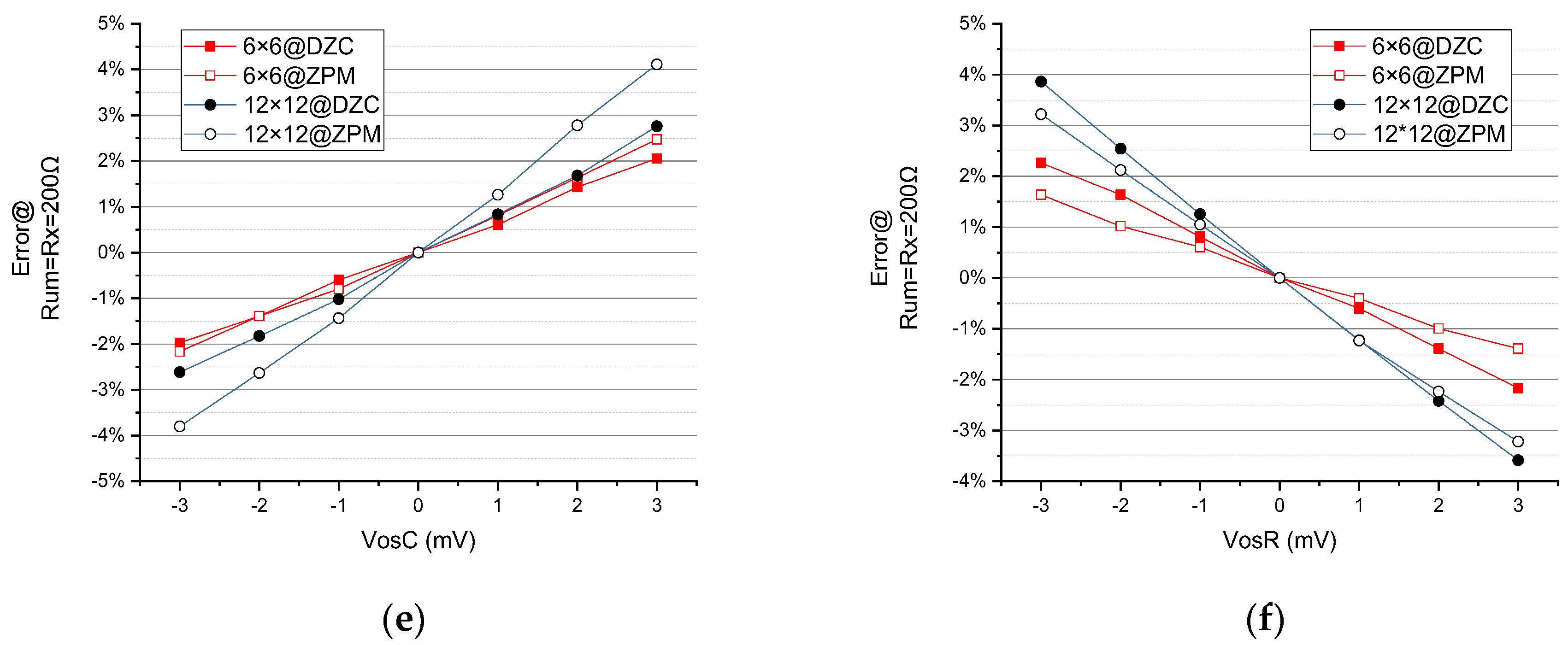
To analyze the system performance with regard to offset voltage, error variation is preferred over absolute error. Absolute error, as discussed in EXP A, can be nulled by manual operation. On the other hand, the fluctuation of e% is non-zero, as (offset voltage of column amplifiers) and (offset voltage of row amplifiers) change. This inconstancy of measurement error often results in temperature drift and process variation of amplifier chips.
Offset voltages exist across the rows and columns in RSA. In the experiment to examine the effect of , is kept constant at zero and changes from −3 mV to 3 mV in steps of 1 mV. Similarly, for the second study to evaluate the influence of , is fixed to zero and is varied from −3 mV to 3 mV in steps of 1 mV.
The offset voltages and are applied to the positive inputs of all row and column amplifiers, labeled as and , respectively (see Figure 4a,b).
Error variation is defined as the difference in measurement error associated with experimental conditions.
As seen in Figure 11a–e, when and change from −3 mV to +3 mV with 1 mV steps, the DZCM (the curve with solid dots) has lower error variation than the ZPM (the curves with open dots) in all array sizes. This reveals that the DZCM is capable of eliminating the adverse effects arising from and of row/column amplifiers. Such improvements can be proven in Equation (5) and Equation (1b), respectively. The DZCM Equation (5) has one less item than ZPM Equation (6). That is because, from Equation (5), the presence of in the DZCM feedback network helps to reduce the effect of offset voltage on the error measurement.

Figure 11.
The effect of (a,c,e) and (b,d,f) on measurement error of different when (EXP D).
As seen in Figure 11f, when changes from −3 mV to +3 mV with 1 mV steps, the DZCM has larger error variation than the ZPM in all array sizes. This reveals that the DZCM is not suitable for high value RSA. However, the error gaps between the DZCM and ZPM decrease with array size increases. This implies the DZCM will have better performance when the high value RSA has a larger array size.
Table 2 shows these performances.
Table 2.
error variation by , with .
3.2. DZCM and ZPM Application on Liquid Metal EGaIn Based Flexible RSA
Figure 12.
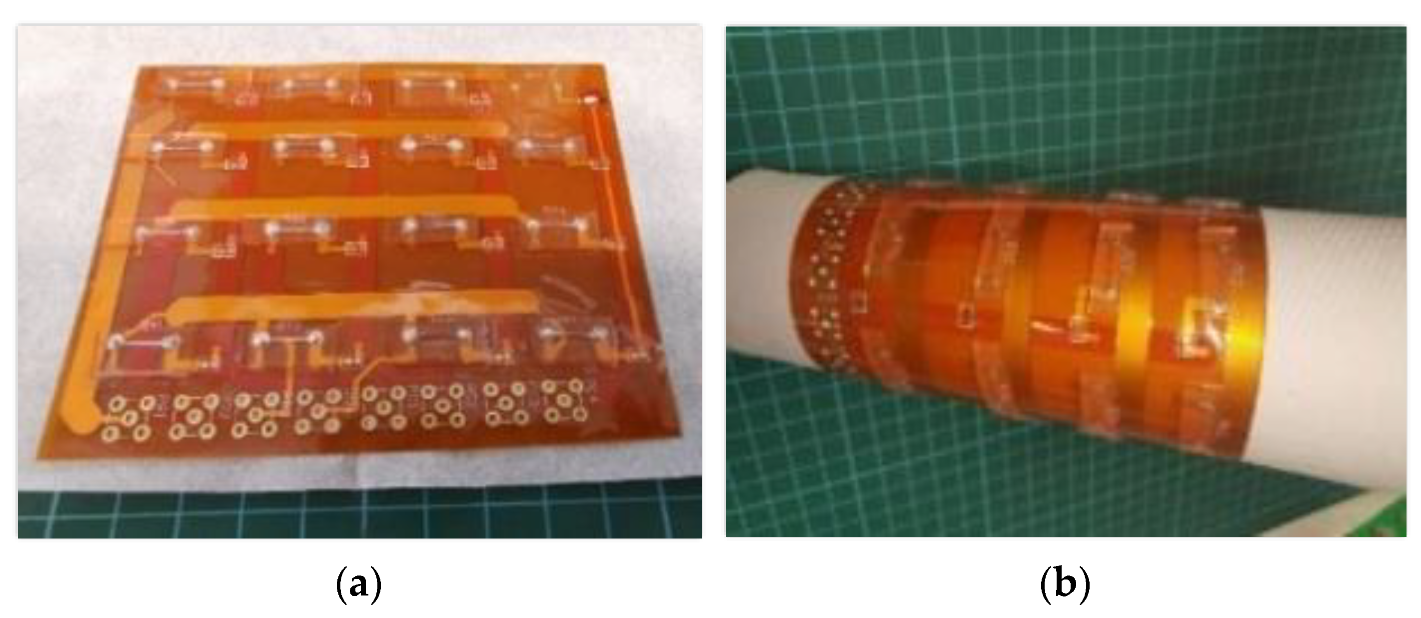
EGaIn based 4 × 4 flexible RSA (a) on flat surface and (b) on bending surface.
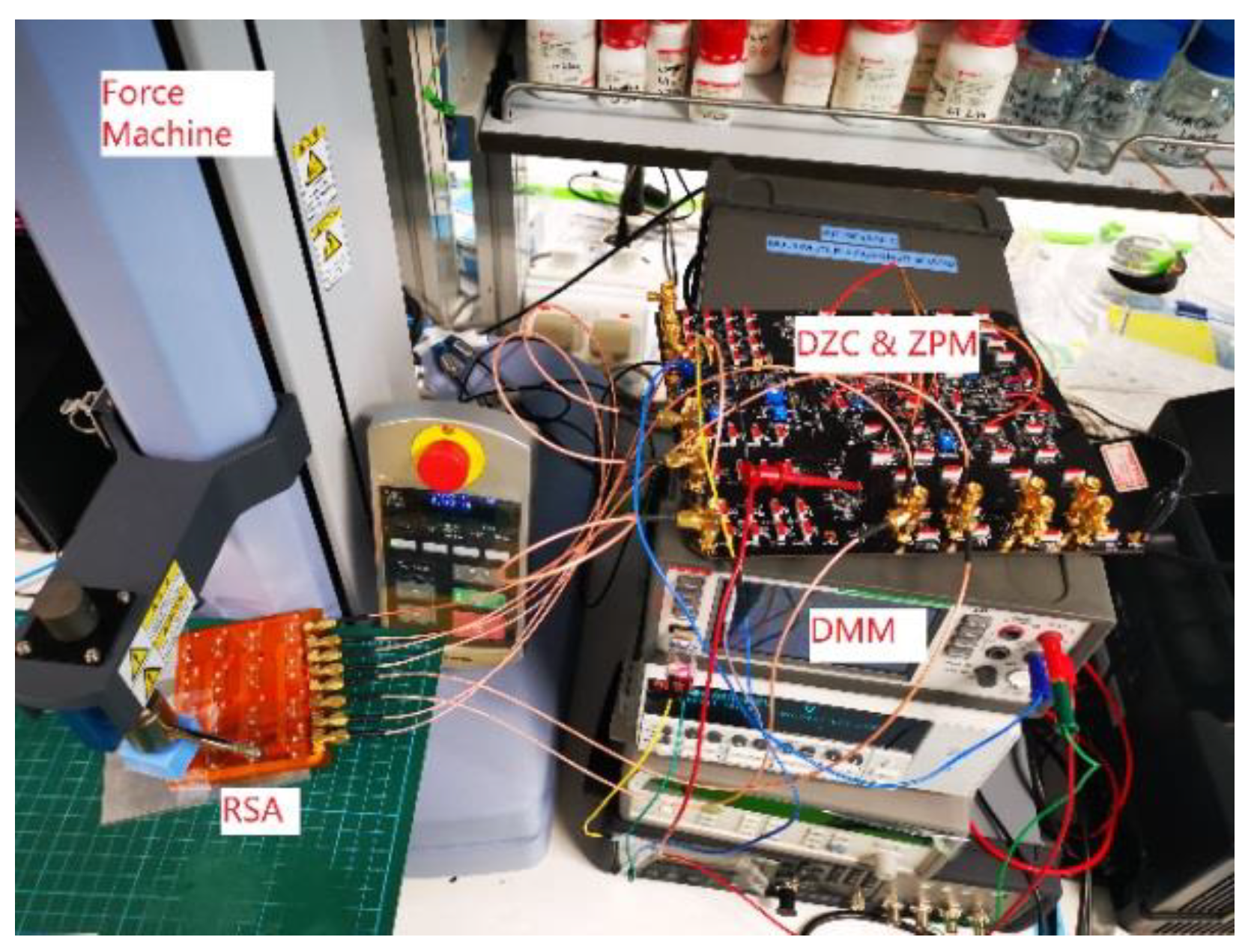
SHIMADZU EZ-SX was used in the mechanical testing to apply 0 N to 2 N loading onto the RSA. A KEITHLEY DMM 6500 digital multimeter was used to measure the single resistor values and the output voltage of DZCM/ZPM circuits. Figure 13 shows the experimental setup.
Figure 13.
Force sensor test bench.
We firstly indented a single independent sensor and measured its resistance directly. This sensor was then connected to a number of other sensors to form a 4 × 4 flexible RSA with DZCM and ZPM readouts. Subsequently, a force was applied onto this particular sensor. Output voltages of the DZCM and ZPM were recorded. These voltage values were converted to resistance by Equation (1).
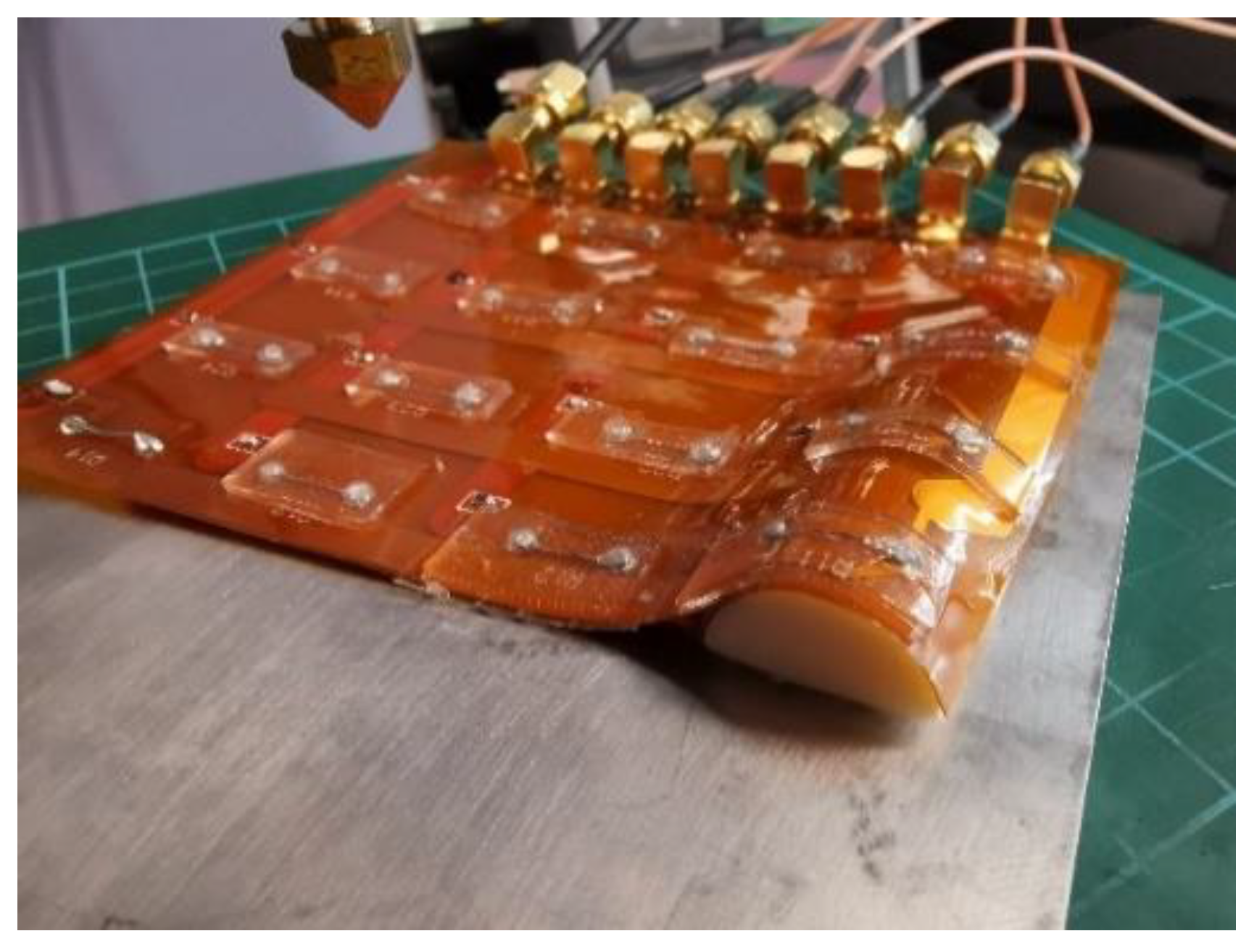
We tested the single sensor and flexible RSA on flat and curved surfaces. The curved surface was shaped by a thumb sized semi-cylinder as shown in Figure 14.
Figure 14.
Flexible sensor mounted onto bending surface with thumb-like size.
In total, we conducted six experiments to assess the performance of the DZCM and its improvement on the actual EGaIn based RSA. The experimental layouts were:
- i.
- Single sensor on a flat surface;
- ii.
- single sensor on a curved surface;
- iii.
- RSA with ZPM on a flat surface;
- iv.
- RSA with ZPM on a curved surface;
- v.
- RSA with DZCM on a flat surface;
- vi.
- RSA with DZCM on a curved surface.
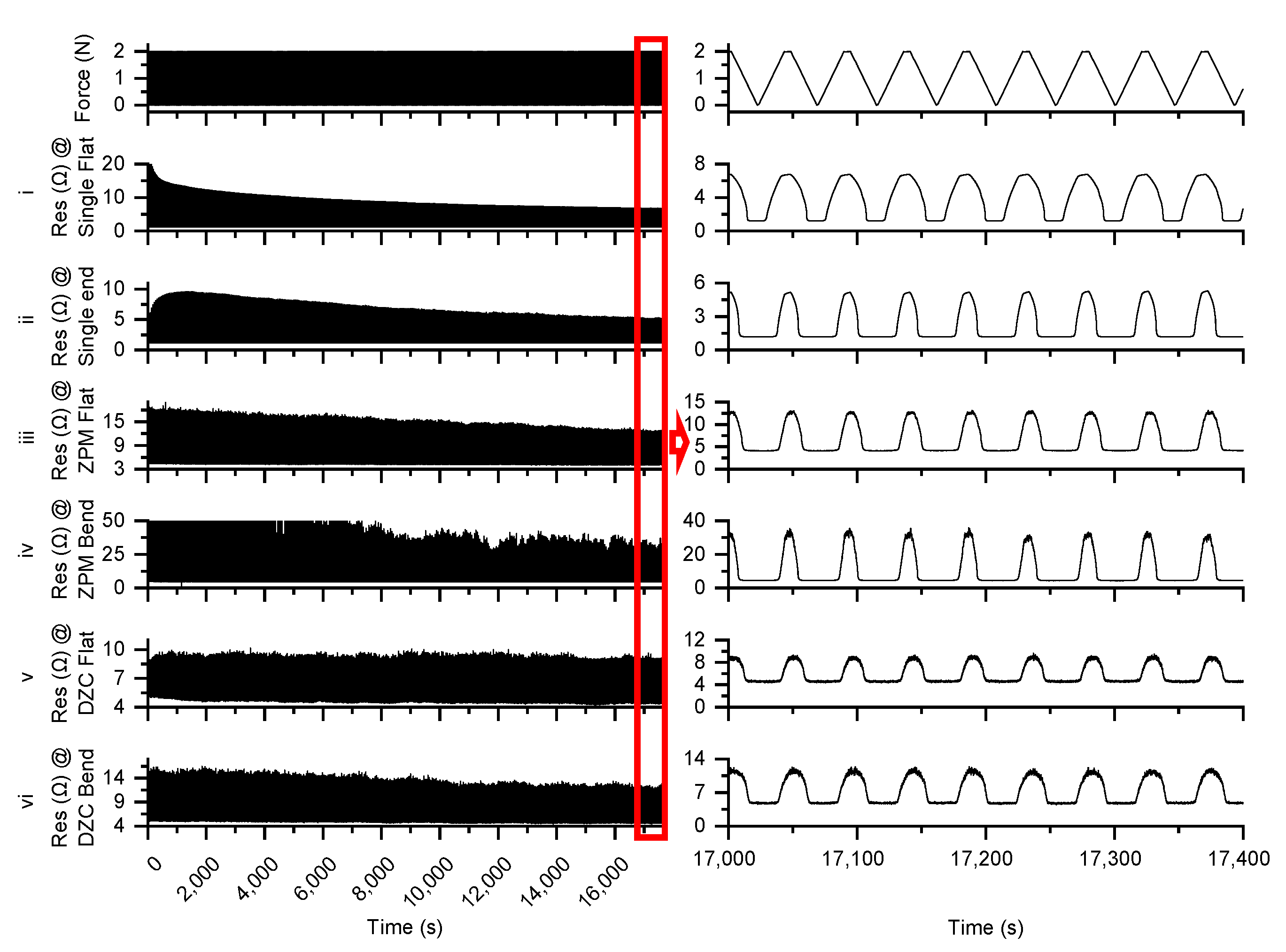
We continuously indented the sensor for about 5 h. Figure 15 shows the 5 h measurement results of the above experiments.
Figure 15.
Five hours of measurement results.
As shown in Figure 15, experiments (i) and (ii) tested only one independent sensor. Both experiments have resistance values that decrease with time and eventually stabilize at 6 Ω on a flat surface and 5 Ω on a curved surface. This is the characteristic of EGaIn based flexible sensors [5]. Experiments (iii) and (iv) tested the RSA with a ZPM readout. The resistance values decreased with time and stabilized at 12 Ω on the flat surface and 30 Ω on the curved surface. Experiments (v) and (vi) tested the RSA with a DZCM readout. The resistance values acquired were the most stable, amounting to 9 Ω on the flat surface and 10 Ω on the curved surface.
From Figure 15, we can conclude two benefits from the DZCM design:
The DZCM has less measurement error than the ZPM on both flat and curved surfaces, especially when the array has low resistor value.
Measurement data from DZCM readout were more stable than that of the ZPM in about 4 h.
3.3. Discussion
It is a challenge to create low value RSAs for low power applications due to the lack of a compatible and stable readout design. Due to the low resistance value and the huge number of resistors involved in an RSA, driving voltage has to be minimized to achieve low power consumption, then the signal level is low. Thus, the noise of the parasitic resistance coming from the connection wires and the input offset voltage of the amplifiers will increase the measurement error greatly. Finally, it leads to a low signal to noise ratio (SNR).
To achieve low power consumption in the RSA, we used: ±2.5 V supply power and 10 mV driving voltage.
To decrease the parasitic wire resistance, we used:
- i.
- Copper wires of 3.6 mm/35 mm/70 µm (width/length/thickness) to connect the resistors to form an RSA on the PCB.
- ii.
- SMA coaxial connector/cable to link RSA PCB to the readout PCB.
- iii.
- Copper wires of 0.15 mm/75 mm/70 µm (width/length/thickness) to connect the SMA connectors and amplifiers on the PCB in the EXP.
To decrease the input offset voltage of amplifiers, we used: OPA4388 with 0.25 µV offset voltage.
As demonstrated in Figure 10 and Figure 11, the DZCM is able to decrease measurement error arising from the parasitic resistance of wires and the input offset voltage of amplifiers. These characteristics of the DZCM, as explained below, are very important to realize steady and reliable wearable applications.
- i.
- The larger physical dimensions of an electrical connection lead to lower parasitic resistance. Nevertheless, the use of bulky connecting wires and connectors in wearable systems is not feasible as they defeat the purpose of making an accessory, which is supposed to be comfortable and easy to wear. The DZCM helps to solve this issue as it has higher tolerance for parasitic resistance. In other words, it enables thinner wires and smaller connectors to be used in the wearable.
- ii.
- The input offset voltage of the amplifier varies with the ambient temperature. Consequently, the measurement result is greatly influenced by the operating environment. The input offset voltage also varies in mass production; thus, the measurement result changes with different product batches. By applying the DZCM, that is less sensitive to the fluctuation of the input offset voltage, these issues can be easily resolved.
The low driving voltage required in the DZCM is another advantage which enables low power consumption. This enhances the wearable’s performance.
The DZCM is cost effective and most likely to be useful in RSA with large array size and high resistance values as well. We did not examine the proposed circuitry in high value RSAs. The crosstalk and parasitic effects have to be quantified to prove its usability. Nonetheless, simulation data in the literature [41] show this tendency.
Lastly, the proposed DZCM design is still in its early stage of development. The measurement error from crosstalk and parasitic resistance is still significant in the readout system. The singular values effect of the DZCM, such as that shown in Figure 8, also requires further improvement.
4. Conclusions
We have discussed the ZPM and established its simplified models to derive the respective output voltage equations. Subsequently, we introduced a new circuit design, called the DZCM, and established a simplified model to deduce its output voltage equations. We also analyzed its measurement performance with different array sizes, input offset voltages of driving amplifier, unmeasured resistance values, parasitic resistance values and resistance value of the resistor of interest. The results show that the DZCM has lower e% than the ZPM. In terms of error variation ratio from amplifier offset voltage, the DZCM has a 4%/mV (row) to 7%/mV (column) ratio, while ZPM has an almost 25%/mV (row) to 45%/mV (column) ratio which increases with array size.
In short, the DZCM is very useful for low value RSAs used in wearable applications. This new circuitry helps to reduce measurement error in the readout system and bring down the material cost for mass production.
5. Patents
One Patent Pending: A circuit to measure low resistor value resistive sensor array with dynamical zero current function (10202204307R).
Author Contributions
Conceptualization, H.Z.; methodology, H.Z.; validation, J.C.T. and J.W.; formal analysis, H.Z. and J.W.; investigation, H.Z.; resources, C.T.L.; data curation, H.Z.; writing—original draft preparation, H.Z. and J.C.T. and L.Y.; writing—review and editing, J.W. and C.T.L.; visualization, H.Z.; supervision, C.T.L.; project administration, C.T.L.; funding acquisition, C.T.L. All authors have read and agreed to the published version of the manuscript.
Funding
This work is supported by the National Innovation Challenge on Active and Confident Ageing (No: MOH/NIC/EIG05A/2017 and MOH/NIC/EIG05B/2017). This work is also supported in part by Shanghai Pujiang Program (22PJ1415300). This work is also supported in part by the Natural Science Foundation of Jiangsu Province under Grant BK20201276.
Institutional Review Board Statement
Not applicable.
Informed Consent Statement
Not applicable.
Data Availability Statement
Not applicable.
Conflicts of Interest
The funders had no role in the design of the study; in the collection, analyses or interpretation of data; in the writing of the manuscript; or in the decision to publish the results.
Appendix A
One ZPM structure is shown in Figure A1. There are one row driving amplifier (rAMP) in each row and one column driving amplifier (cAMP) in each column. Resistor (i = 1, 2, 3, 4) is connected to two amplifiers on each of its nodes. The resistor is driven to by rAMP1 and grounded by cAMPi. is generated by cAMPi which drives one node of to ground.
Figure A1.
Circuit based on the ZPM.
Two nodes of the other adjacent unmeasured resistors ( to ) are grounded through their connected rAMP and cAMP. The example is in Figure A1, and these resistors have zero potential difference, thus there will be no current flow through . Then, the crosstalk current flowing through will be cut off. The ideal measurement value can be computed from Equation (A1).
is the measured resistor, is the input voltage to drive the measured resistor, is the current of the feedback resistor of the column amplifier, is the output voltage of the column amplifier.
In the case of an actual hardware system, the parasitic effect must be taken into consideration. The ON state switch resistor () and the amplifier offset voltage (, ) are included in the calculation. To include the parasitic effect and explain the characteristics of the ZPM, we simplify the network to just one resistor . The revised circuit is shown in Figure A2.
Figure A2.
Circuit designs that include parasitic effects in the cases of ZPM.
The measurable resistance in Equation (A1) is modified and the new equations are depicted in Equation (A2):
Figure A3 shows an example of a 2 × 2 RSA, taking into account both the crosstalk and parasitic effect. In order to include non-ideal factors (row and column parasitic resistance and amplifier offset voltage ) in this model, we use the ZPM for the analysis below. Non-ideal factors are illustrated as and in the circuit model.
Figure A3.
A 2 × 2 array circuit model including parasitic and crosstalk current effects for ZPM.
To calculate the intrinsic crosstalk current effect, we first extract the array network and apply Kirchhoff’s law, as shown in Figure A4 and Equation (A3).
Figure A4.
Array network extracted and analyzed with Kirchhoff’s law.
We hypothesize and and . After substituting (A3a, A3b, A3c, A3d) with (A3e, A3f, A3g, A3h), we obtain Equation (A4).
Equation (A4) is a non-homogeneous linear equation and can be written as Equation (A5).
We define and, then we have:
After rearranging the linear equation, we have:
From (A3-1), we have . Deriving from (A7) row 1 () and row 3 (), and after simplifying, we have:
We can now evaluate from Equation (A8) by assuming , , , and are all equal to zero (ideal case). Equation (A8) is then modified as and it matches with Equation (A1).
Appendix B
Equation (3) is a non-homogeneous linear equation and can be written as Equation (A9a).
After defining and and , we have:
Rearranging row 1, we have:
Rearranging row 2, we have:
From Equation (2a), we have . From Equation (A9d) row 1 (), we have:
References
- Dickey, M.D. Stretchable and Soft Electronics using Liquid Metals. Adv. Mater. 2017, 29, 1606425. [Google Scholar] [CrossRef] [PubMed]
- Cheng, S.; Wu, Z. A Microfluidic, Reversibly Stretchable, Large-Area Wireless Strain Sensor. Adv. Funct. Mater. 2011, 21, 2282–2290. [Google Scholar] [CrossRef]
- Roberts, P.; Damian, D.D.; Shan, W.; Lu, T.; Majidi, C. Soft-matter capacitive sensor for measuring shear and pressure deformation. In Proceedings of 2013 IEEE International Conference on Robotics and Automation, Karlsruhe, Germany, 6–10 May 2013; pp. 3529–3534. [Google Scholar] [CrossRef]
- Vogt, D.M.; Park, Y.-L.; Wood, R.J. Design and Characterization of a Soft Multi-Axis Force Sensor Using Embedded Microfluidic Channels. IEEE Sens. J. 2013, 13, 4056–4064. [Google Scholar] [CrossRef]
- Yeo, J.C.; Yu, J.; Koh, Z.M.; Wang, Z.; Lim, C.T. Wearable tactile sensor based on flexible microfluidics. Lab Chip 2016, 16, 3244–3250. [Google Scholar] [CrossRef] [PubMed]
- Yeo, J.C.; Kenry; Yu, J.; Loh, K.P.; Wang, Z.; Lim, C.T. Triple-State Liquid-Based Microfluidic Tactile Sensor with High Flexibility, Durability, and Sensitivity. ACS Sens. 2016, 1, 543–551. [Google Scholar] [CrossRef]
- Yu, L.; Yeo, J.C.; Soon, R.H.; Yeo, T.; Lee, H.H.; Lim, C.T. Highly Stretchable, Weavable, and Washable Piezoresistive Microfiber Sensors. ACS Appl. Mater. Interfaces 2018, 10, 12773–12780. [Google Scholar] [CrossRef]
- Snyder, W.E.; Clair, J.S. Conductive Elastomers as Sensor for Industrial Parts Handling Equipment. IEEE Trans. Instrum. Meas. 1978, 27, 94–99. [Google Scholar] [CrossRef]
- Prutchi, D.; Arcan, M. Dynamic contact stress analysis using a compliant sensor array. Measurement 1993, 11, 197–210. [Google Scholar] [CrossRef]
- Tanaka, A.; Matsumoto, S.; Tsukamoto, N.; Itoh, S.; Chiba, K.; Endoh, T.; Nakazato, A.; Okuyama, K.; Kumazawa, Y.; Hijikawa, M.; et al. Infrared focal plane array incorporating silicon IC process compatible bolometer. IEEE Trans. Electron Devices 1996, 43, 1844–1850. [Google Scholar] [CrossRef]
- Takei, K.; Takahashi, T.; Ho, J.C.; Ko, H.; Gillies, A.G.; Leu, P.W.; Fearing, R.S.; Javey, A. Nanowire active-matrix circuitry for low-voltage macroscale artificial skin. Nat. Mater. 2010, 9, 821–826. [Google Scholar] [CrossRef]
- Wang, C.; Hwang, D.; Yu, Z.; Takei, K.; Park, J.; Chen, T.; Ma, B.; Javey, A. User-interactive electronic skin for instantaneous pressure visualization. Nat. Mater. 2013, 12, 899–904. [Google Scholar] [CrossRef] [PubMed]
- Kane, B.J.; Cutkosky, M.R.; Kovacs, G.T.A. A traction stress sensor array for use in high-resolution robotic tactile imaging. J. Microelectromechanical Syst. 2000, 9, 425–434. [Google Scholar] [CrossRef]
- Vidal-Verdú, F.; Oballe-Peinado, Ó.; Sánchez-Durán, J.A.; Castellanos-Ramos, J.; Navas-González, R. Three realizations and comparison of hardware for piezoresistive tactile sensors. Sensors 2011, 11, 3249–3266. [Google Scholar] [CrossRef]
- Oballe-Peinado, Ó.; Vidal-Verdú, F.; Sánchez-Durán, J.A.; Castellanos-Ramos, J.; Hidalgo-López, J.A. Accuracy and resolution analysis of a direct resistive sensor array to FPGA interface. Sensors 2016, 16, 181. [Google Scholar] [CrossRef] [PubMed]
- Oballe-Peinado, Ó.; Vidal-Verdú, F.; Sánchez-Durán, J.A.; Castellanos-Ramos, J.; Hidalgo-López, J.A. Improved circuits with capacitive feedback for readout resistive sensor arrays. Sensors 2016, 16, 149. [Google Scholar] [CrossRef]
- Shu, L.; Tao, X.; Feng, D.D. A new approach for readout of resistive sensor arrays for wearable electronic applications. IEEE Sens. J. 2014, 15, 442–452. [Google Scholar] [CrossRef]
- Hidalgo-Lopez, J.A.; Romero-Sánchez, J.; Fernández-Ramos, R. New approaches for increasing accuracy in readout of resistive sensor arrays. IEEE Sens. J. 2017, 17, 2154–2164. [Google Scholar] [CrossRef]
- López, J.A.H.; Oballe-Peinado, Ó.; Sánchez-Durán, J.A. A proposal to eliminate the impact of crosstalk on resistive sensor array readouts. IEEE Sens. J. 2020, 20, 13461–13470. [Google Scholar] [CrossRef]
- Lorussi, F.; Rocchia, W.; Scilingo, E.P.; Tognetti, A.; De Rossi, D. Wearable, redundant fabric-based sensor arrays for reconstruction of body segment posture. IEEE Sens. J. 2004, 4, 807–818. [Google Scholar] [CrossRef]
- Tise, B. A compact high resolution piezoresistive digital tactile sensor. In Proceedings of the 1988 IEEE International Conference on Robotics and Automation, Philadelphia, PA, USA, 24–29 April 1988; pp. 760–764. [Google Scholar] [CrossRef]
- Speeter, T.H. Flexible, piezoresitive touch sensing array. In Proceedings of the Optics, Illumination, and Image Sensing for Machine Vision III, Boston, MA, USA, 7–11 November 1988; pp. 31–43. [Google Scholar]
- Speeter, T.H. A tactile sensing system for robotic manipulation. Int. J. Robot. Res. 1990, 9, 25–36. [Google Scholar] [CrossRef]
- Liu, H.; Zhang, Y.-F.; Liu, Y.-W.; Jin, M.-H. Measurement errors in the scanning of resistive sensor arrays. Sens. Actuators A Phys. 2010, 163, 198–204. [Google Scholar] [CrossRef]
- D’Alessio, T. Measurement errors in the scanning of piezoresistive sensors arrays. Sens. Actuators A Phys. 1999, 72, 71–76. [Google Scholar] [CrossRef]
- Jianfeng, W.; Lei, W.; Jianqing, L.; Zhongzhou, Y. A small size device using temperature sensor array. Chin. J. Sens. Actuators 2011, 24, 1649–1652. [Google Scholar]
- Wu, J.; Wang, L.; Li, J. Design and crosstalk error analysis of the circuit for the 2-D networked resistive sensor array. IEEE Sens. J. 2014, 15, 1020–1026. [Google Scholar] [CrossRef]
- Wu, J.; Wang, L.; Li, J.; Song, A. A novel crosstalk suppression method of the 2-D networked resistive sensor array. Sensors 2014, 14, 12816–12827. [Google Scholar] [CrossRef] [PubMed]
- Wu, J.; He, S.; Li, J.; Song, A. Cable crosstalk suppression with two-wire voltage feedback method for resistive sensor array. Sensors 2016, 16, 253. [Google Scholar] [CrossRef] [PubMed]
- Wu, J.; Wang, L.; Li, J. General voltage feedback circuit model in the two-dimensional networked resistive sensor array. J. Sens. 2015, 2015, 913828. [Google Scholar] [CrossRef]
- Lazzarini, R.; Magni, R.; Dario, P. A tactile array sensor layered in an artificial skin. In Proceedings of the 1995 IEEE/RSJ International Conference on Intelligent Robots and Systems. Human Robot Interaction and Cooperative Robots, Pittsburgh, PA, USA, 5–9 August 1995; pp. 114–119. [Google Scholar] [CrossRef]
- Saxena, R.S.; Bhan, R.K.; Saini, N.K.; Muralidharan, R. Virtual ground technique for crosstalk suppression in networked resistive sensors. IEEE Sens. J. 2010, 11, 432–433. [Google Scholar] [CrossRef]
- Yarahmadi, R.; Safarpour, A.; Lotfi, R. An improved-accuracy approach for readout of large-array resistive sensors. IEEE Sens. J. 2015, 16, 210–215. [Google Scholar] [CrossRef]
- Wu, J.; Wang, L. Cable crosstalk suppression in resistive sensor array with 2-wire S-NSDE-EP method. J. Sens. 2016, 2016, 8051945. [Google Scholar] [CrossRef]
- Kim, J.-S.; Kwon, D.-Y.; Choi, B.-D. High-accuracy, compact scanning method and circuit for resistive sensor arrays. Sensors 2016, 16, 155. [Google Scholar] [CrossRef] [PubMed]
- Wu, J.; Wang, Y.; Li, J.; Song, A. A novel two-wire fast readout approach for suppressing cable crosstalk in a tactile resistive sensor array. Sensors 2016, 16, 720. [Google Scholar] [CrossRef] [PubMed]
- Wu, J.; Li, J. Approximate model of zero potential circuits for the 2-D networked resistive sensor array. IEEE Sens. J. 2016, 16, 3084–3090. [Google Scholar] [CrossRef]
- Manapongpun, P.; Bunnjaweht, D. An Enhanced Measurement Circuit for Piezoresistive Pressure Sensor Array. In Proceedings of the 2020 17th International Conference on Electrical Engineering/Electronics, Computer, Telecommunications and Information Technology (ECTI-CON), Phuket, Thailand, 24–27 June 2020; pp. 105–108. [Google Scholar] [CrossRef]
- Warnakulasuriya, A.S.; Dinushka, N.Y.; Dias, A.A.C.; Ariyarathna, H.P.A.R.; Ramraj, C.; Jayasinghe, S.; Silva, A.C.D. A Readout Circuit Based on Zero Potential Crosstalk Suppression for a Large Piezoresistive Sensor Array: Case Study Based on a Resistor Model. IEEE Sens. J. 2021, 21, 16770–16779. [Google Scholar] [CrossRef]
- Hu, Z.; Tan, W.; Kanoun, O. High Accuracy and Simultaneous Scanning AC Measurement Approach for Two-Dimensional Resistive Sensor Arrays. IEEE Sens. J. 2019, 19, 4623–4628. [Google Scholar] [CrossRef]
- Wu, J.-F.; Li, J.-Q.; Song, A.-G. Readout circuit based on double voltage feedback loops in the two-dimensional resistive sensor array: Design, modelling and simulation evaluation. IET Sci. Meas. Technol. 2017, 11, 288–296. [Google Scholar] [CrossRef]
Disclaimer/Publisher’s Note: The statements, opinions and data contained in all publications are solely those of the individual author(s) and contributor(s) and not of MDPI and/or the editor(s). MDPI and/or the editor(s) disclaim responsibility for any injury to people or property resulting from any ideas, methods, instructions or products referred to in the content. |
© 2023 by the authors. Licensee MDPI, Basel, Switzerland. This article is an open access article distributed under the terms and conditions of the Creative Commons Attribution (CC BY) license (https://creativecommons.org/licenses/by/4.0/).