Abstract
The estimation of the characteristic parameters of the electrical contacts in CdZnTe and CdTe detectors is related to the identification of the main transport mechanisms dominating the currents. These investigations are typically approached by modelling the current–voltage (I–V) curves with the interfacial layer–thermionic-diffusion (ITD) theory, which incorporates the thermionic emission, diffusion and interfacial layer theories into a single theory. The implementation of the ITD model in measured I–V curves is a critical procedure, requiring dedicated simplifications, several best fitting parameters and the identification of the voltage range where each transport mechanism dominates. In this work, we will present a novel method allowing through a simple procedure the estimation of some characteristic parameters of the metal–semiconductor interface in CdZnTe and CdTe detectors. The barrier height and the effects of the interfacial layer will be evaluated through the application of a new function related to the differentiation of the experimental I–V curves.
1. Introduction
Currently, cadmium telluride (CdTe) and cadmium zinc telluride (CZT or CdZnTe) detectors represent very appealing products for X-ray and gamma ray detection [1,2,3,4], allowing sub-keV energy resolution near room-temperature conditions [5,6,7,8]. Low leakage currents (<1 nA) from the detectors are mandatory for excellent room temperature performance and optimal matching with low noise preamplifiers [5]. Generally, the leakage currents are controlled by both the bulk resistivity of the material and the electrical contacts [9,10,11,12,13]; the bulk resistivity dominates the currents at low voltages, the electrical contacts at high voltages. Typically, high-resolution CZT detectors are fabricated with quasi-ohmic electroless contacts (platinum, gold electrodes) [9,13,14,15,16], showing symmetric current–voltage (I–V) curves. CdTe detectors are equipped with rectifying contacts (indium [17], aluminium [18,19]), characterized by asymmetric I–V curves and very low currents at reverse bias; despite this, temporal instabilities, due to bias-induced polarization phenomena [2,8,19,20,21,22], must be taken into account, especially at high temperatures. Recently, very low leakage currents were obtained in new high-flux HF-CZT detectors designed for high flux measurements; these detectors are equipped with sputtered platinum contacts, showing asymmetric I–V curves and no temporal instabilities [7,23,24,25,26,27,28].
The analysis of the I–V characteristics under dark conditions is a consolidated technique to characterize the quality of the electrical contacts. This technique allows for the identification of the main transport mechanisms dominating the currents and the estimation of some characteristic parameters of the metal–semiconductor junction. The knowledge of these parameters can be useful to improve the quality of the detector metal contacts. The currents are dominated by different carrier transport mechanisms depending on the voltage range. At high reverse-bias voltages, the leakage current is characterized by the Schottky barrier of the metal–semiconductor junction. The transport mechanisms of the electrical contacts of CdTe and CZT detectors are typically investigated by using the interfacial layer–thermionic-diffusion (ITD) theory [29,30]. This model combines the thermionic emission, diffusion and interfacial layer theories into a single theory. The model adds the effects of an insulating oxide layer between the metal and the semiconductor material, generally formed during the contact deposition. The ITD modelling was successfully applied in the analysis of the I–V curves of several CZT detectors (Pt/CZT/Pt [29,31], Au/CZT/Au [9,13,15,32]).
The implementation of the ITD model in the measured I–V curves is a complex procedure, mainly due to the difficulties in correctly identifying the voltage range where each transport mechanism dominates; moreover, the modelling often requires custom simplifications and a high number of characteristic parameters, leading to overfitting and cumbersome procedures.
In this work, we will present a simple and useful method allowing for the estimation of some characteristic parameters of the metal–semiconductor interface in CZT and CdTe detectors. The method is based on the use of a new function related to the differentiation of the I–V curves. After a quick introduction t the ITD theory, we will describe the main characteristics of the new function (H function) applied to calculated I–V curves following the ITD model. The results from the H function method applied to the experimental I–V curves of different CZT and CdTe detectors will be shown.
2. Overview of the Interfacial Layer–Thermionic-Diffusion (ITD) Theory
The modelling of the I–V curves of CZT and CdTe detectors, the identification of the main transport mechanisms and the estimation of the characteristic parameters of the electrical contacts are typically performed by using the ITD theory [29,30]. This model, beside the thermionic-diffusion mechanism, includes the presence of an interfacial layer and its voltage drop, which can lead to a lowering of the barrier height. Typically, the detectors are modelled as metal–semiconductor–metal (MSM) systems, with two back-to-back Schottky barriers [29]. At high voltages, where the detectors are fully depleted, the transport mechanism is dominated by one of the two junctions, with a current density J expressed as follows [30]:
where:
- θ with 0 ≤ θ ≤ 1 is the transmission coefficient across the interfacial layer (θn for majority carriers represented by electrons, θh for holes); θ is related to the thickness of the interfacial layer and the effective barrier height presented by the thin interfacial layer;
- ϕB0 is the barrier height under thermal equilibrium conditions of the metal–semiconductor junction;
- A* is the is the effective Richardson constant of the majority charge carriers;
- VTH = k T/q, where k is the Boltzmann constant, T the absolute temperature and q the electron charge;
- VR = A* T2/qNx is the thermal velocity in the current flow direction; Nx is the effective density of states (x = v for valence and x = c for conduction band);
- VD is the effective diffusion velocity, associated with the transport of the majority carriers from the edge of the depletion layer to the potential peak;
- C2= ϵi/(ϵi + q2Ds δ), where ϵi = ϵr ϵ0 and δ are the permittivity and thickness of the interfacial layer and Ds is the density of surface states per unit energy and area; this parameter characterizes the barrier lowering due to the voltage drop across the interfacial layer.
A critical issue in modelling the measured I–V curves with Equation (1) is represented by the relation between VD and the bias voltage. In Ref. [30], the analytical expression for VD is reported for the electrons, which includes the voltage drop across the interfacial layer and the transmission coefficient of carriers across the interfacial layer. This expression involves the electrostatic potential profile in the depleted region. In Ref. [29], a simplified expression for VD is used, as follows:
where µn is the electron mobility and Ec is the electric field at the cathode, which is assumed to depend linearly on the reverse bias voltage. The parameter C2 characterizes the voltage drop across the interfacial layer, C2 V, which gives the additional barrier height lowering. C2 is assumed to be independent by the temperature [29]. When the density of surface states Ds → ∞, then C2 → 1, and in this case the Fermi level at the interface is pinned at a value Φ0 above the valence band by the surface states and the barrier height seen by electrons is ϕBn = Eg − Φ0, where Eg is the band gap of the semiconductor. In this case, the barrier height is independent of the metal work function. When Ds → 0, ϕBn = φm − χ, where φm is the metal work function and χ the electron affinity of the semiconductor. Typical C2 values in CZT detectors are of the order of 10−5 and 10−4 [15,29,31,32]. Figure 1 shows the simplified schematic diagrams of the metal/n-CZT (a) and metal/p-CdTe (b) interface, at thermodynamic equilibrium.
VD = µn Ec,
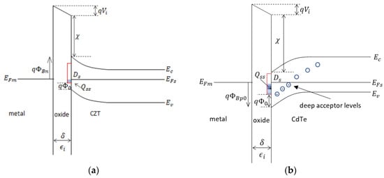
Figure 1.
Schematic energy band diagram at the thermal equilibrium of the n-type CZT (a) and (b) p-type CdTe contacts, with an interfacial layer of the order of atomic distance. Uniform distribution of acceptor-type surface states with density Ds. The surface state charge density is Qss = −q Ds (Eg − qΦ0). For the CdTe are indicated the deep acceptor levels responsible for polarization. The image force-induced lowering is neglected.
The ITD theory foresees two extreme cases:
- (i)
- If θ VR << VD, the leakage current is dominated by the thermionic emission (TE) and Equation (1) can be approximated to:
- (ii)
- If θ VR >> VD, the leakage current is dominated by the diffusion (D) mechanism and can be presented as:
If the interfacial layer is not present (i.e., θ = 1 and C2 = 0) or its effect is negligible, the leakage current is diffusion-limited to high-bias voltages that show quasi-ohmic behaviour, with effective resistivity higher than the bulk one [29].
3. Estimation of the Characteristic Parameters of Electrical Contacts: The Role of the H Function
The ITD modelling of the measured I–V curves of CZT and CdTe detectors is very helpful for the estimation of the characteristic parameters of the electrical contacts. However, the implementation of the ITD model often results in a complex fitting procedure, characterized by several free parameters, requiring dedicated simplifications and the selection of the proper voltage/temperature range for each dominant mechanism. In order to simplify the parameter estimation, we defined a new function, termed the H function, expressed as follows:
By applying the H function on the I–V curves modelled with the ITD theory (Equation (1)), we obtain:
If the TE mechanism dominates the current, the H function can be approximated as follows:
H (V,T) = C2
This result highlights that the presence of the plateau zone on the H function can allow for the simple and well-defined identification of the TE voltage range. Therefore, the behaviour of the H–V curves can be used to estimate the C2 parameter and identify the I–V zone dominated by the TE mechanism. The knowledge of both C2 and the current values in the TE regime is key in the estimation of further characteristic parameters of the electrical contacts. The slope and the intercept of the linear Arrhenius plots of ln(J/T2) − C2V/VTH versus q/KT (from Equation (3)) give the estimation of the barrier height φB0 and the product A*θ. Hence, the H function allows us to determine the TE voltage range and estimation of the characteristic parameters by taking into account the barrier lowering (through the parameter C2).
To better highlight the potentialities of the H function, we calculated some I–V curves expected from the ITD theory (Equation (1)). We used the characteristic parameters of Pt/CZT/Pt detectors [29], as reported in Table 1.

Table 1.
Characteristic parameters of the electrical contacts of Pt/CZT/Pt detectors [29], used in the calculated ITD current–voltage curves. The parameters were estimated in the reverse-current regime.
The ratio θ VR/VD, the resistance RS = V/I and the H function vs. the voltage were calculated at different temperatures. The calculated I–V curves, presented in Figure 2a, highlight a linear trend up to about 1000 V, followed by an exponential trend. The ratio θ VR/VD is always <1 and it decreases at high voltages (Figure 2b). This indicates that the currents are dominated by the TE mechanism. The Rs–V curves (Figure 2c) present a maximum value at the voltage Vmax = VTH/C2, as expected from the TE regime. This allows another possible approach in C2 estimation. The H–V curves (Figure 2d) clearly show the expected plateau zone, giving a C2 value equal to the settled one (Table 1, C2 = 2.5·10−5). Both the ratio θ VR/VD and the H function are quite independent from the temperature. We also estimated C2 from the Rs–V curves, obtaining C2 = 2.6·10−5.
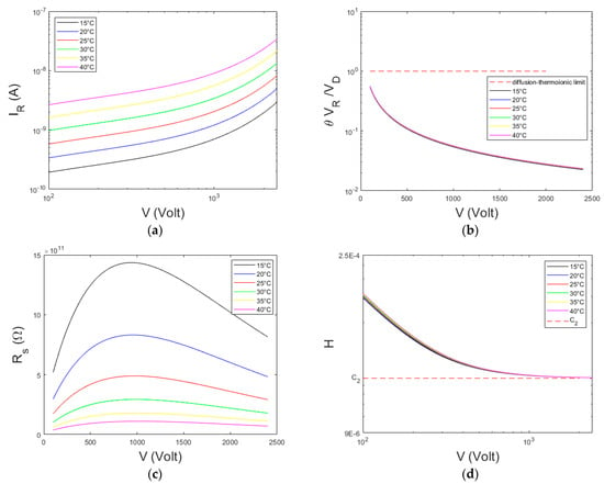
Figure 2.
(a) Calculated I−V curves following the ITD model (Equation (1)) for a Pt/CZT/Pt detector (Table 1). (b) The ratio θ VR/VD vs. the voltage, (c) The Rs−V curves. (d) The calculated H−V curves. The results are presented at different temperatures and by using a transmission coefficient θ = 0.05.
This small discrepancy is due to the Vmax value, positioned in a voltage zone where the dominance of the mechanism is not marked. Figure 3 shows the Arrhenius plots of ln(J/T2) − C2V/VTH versus q/KT, calculated at different bias voltages, where TE dominates. The curves are independent of the bias voltage, giving through the slope and the intercept a correct estimation of the barrier height qφB0 and the transmission coefficient θ, in perfect agreement with the settled data of Table 1.
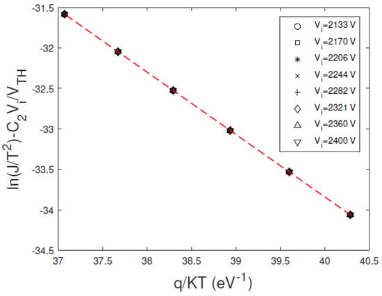
Figure 3.
Calculated Arrhenius plots of ln(J/T2) − C2V/VTH versus q/KT, at different bias voltages. The voltages belong to the voltage range where the H−V curve reaches a plateau (dominant TE regime). We used a transmission coefficient θ = 0.05.
As comparison, we also calculated the I–V curves and related quantities by using a greater transmission coefficient θ = 0.5. In this case, the diffusion component gives higher contribution to calculated currents. The results are shown in Figure 4. The H function does not reach a well-defined plateau (Figure 4d), obtaining C2 = 2.7·10−5. The maximum of the Rs curves occur at low voltages, obtaining C2 = 5.4·10−5, very different from the settled value (C2 = 2.5·10−5).
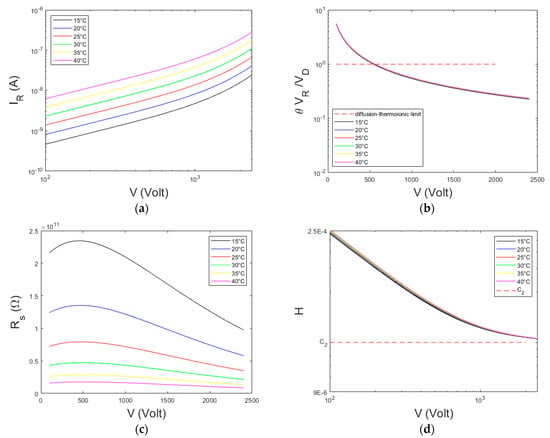
Figure 4.
(a) Calculated I–V curves following the ITD model (Equation (1)) for a Pt/CZT/Pt detector (Table 1). (b) The ratio θ VR/VD vs. the voltage, (c) The Rs–V curves. (d) The calculated H–V curves. The results are presented at different temperatures and by using a transmission coefficient θ = 0.5.
From the Arrhenius plots of Figure 5 we obtained qφB0 in perfect agreement with the settled data of Table 1, while a transmission coefficient θ = 0.35 was estimated.
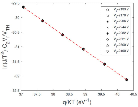
Figure 5.
Calculated Arrhenius plots of ln(J/T2) − C2V/VTH versus q/KT, at different bias voltages. The voltages belong to the voltage range where the H–V curve reaches a quasi-plateau. We used a transmission coefficient θ = 0.5.
Generally, the estimation of the C2 parameter is more accurate for the H function approach, and the differences between the two methods are more marked when the diffusion contribution increases.
4. Materials and Methods
We applied the proposed H function method to measured I–V curves of different CZT and CdTe detectors. The first sample (D1 detector) is based on a low flux LF-CZT crystal (4.1 × 4.1 × 3 mm3), grown using the traveling heater method (THM) technique (Redlen Technologies, Saanichton BC, Canada); it was fabricated at the IMEM-CNR Institute (Parma, Italy) by using gold electroless contacts. Recently, very-low-noise gold contacts were realized on CZT detectors by our group [14,15,23,25,26,33], ensuring low leakage currents at room temperature (4.7 nA cm−2 at 1000 V cm−1) and good room-temperature operation, even at high bias voltages (>5000 V cm−1). The LF-CZT crystals are characterized by mobility–lifetime products μeτe ranging from 1 to 3·10−2 cm2/V and μhτh from 2 to 3·10−5 cm2/V [21,32,33], mainly used for electron-sensing detectors working at low flux conditions [14,34,35,36,37,38]. The anode layout is characterized by a central pixel (2 × 2 mm2) surrounded by a guard ring. The width of the guard ring is 950 μm, and the gap between the pixel and the guard ring is 50 μm. The cathode is a planar electrode covering the overall detector surface (4.1 × 4.1 mm2).
The second sample (D2 detector) was also realized at the IMEM-CNR Institute; it is based on a high-flux HF-CZT crystal (5 × 5 × 1.5 mm3) with sputtered platinum (Pt) electrical contacts. Recently, HF-CZT crystals grown using the THM technique are developed by Redlen. These crystals, characterized by enhanced hole charge transport properties (μeτe ranging from 2 to 3·10−3 cm2/V and μhτh from 1 to 2·10−4 cm2/V [23]), are very appealing for high flux measurements [23,24,25,26,27,28]. The detector has a full-area cathode with the Pt contact and a customized pixelated Pt anode (2 × 2 array; pixel size 500 × 500 μm2, with 200 μm gap). The pixels are surrounded by a guard ring.
The third sample (D3 detector) is based on a CdTe crystal (4.1 × 4.1 × 2 mm3), manufactured by Acrorad (Japan). The anode and cathode geometries are identical to the D1 detector ones. The detector is characterized by the Al/CdTe/Pt electrode configuration. High-resolution performances were generally obtained with Al/CdTe/Pt detectors at low X-ray energies (<100 keV) by using moderate cooling and taking into account polarization effects [2,8,19,20,21,39,40,41].
The main characteristics of the detectors are summarized in Table 2.

Table 2.
Main characteristics of the detectors used for the I–V measurements.
The I–V curves of these detectors were measured with the Keithley 2410 and CAEN NDT1471 instruments, providing the cathode bias voltage. The Keithley 2635B, configured as an electrometer and connected to the pixel anode, was used to measure the leakage current (accuracy < 0.2%). The guard-ring electrodes are forced to the ground potential. I–V measurements were performed in both reverse (i.e., by applying negative voltages to the full-area electrodes) and in forward biasing. All measurements were performed with the detectors enclosed in a shielded box under a nitrogen atmosphere with a temperature control system. To minimize the polarization effects in the CdTe detector (D3 detector), a dedicated procedure was used by resetting the bias voltage between two consecutive measurements.
5. Measurements and Results
5.1. Experimental Current-Voltage (I–V) Curves
Figure 6 shows the I–V curves of the investigated detectors at different temperatures, measured in reverse (left column) and forward (right column) biasing. The D1 detector (Au/LF-CZT/Au, electroless deposition) is characterized by quasi-symmetric current curves, typically observed in Au/CZT/Au detectors with electroless contacts [15,32]. At low voltages, the current follows a power law trend ∝ Vb, with b = 0.8 in reverse (Figure 6a) and b = 0.9 in forward (Figure 6b). At high voltages the current increases with a higher slope (b > 2), both in reverse and forward, typical of the space charge limited current (SCLC) regime [32]. The starting voltage of the SCLC regime depends on the temperature. The D2 detector (Pt/HF-CZT/Pt, sputter deposition) shows asymmetric I–V curves, typical of CZT detectors with sputter Pt contacts [7], with forward-biasing currents (Figure 6d) higher than the reverse-biasing ones (Figure 6c). The transport mechanism in reverse is governed by a reversed-biased Schottky barrier, with the ITD model able to be applied. The reverse current follows a trend ∝ V at all temperatures, typical of the diffusion mechanism. Asymmetric I–V curves were also measured for the D3 detector (Al/CdTe/Pt), in agreement with the well-known rectifying properties of Al/CdTe/Pt detectors [18,19,41]. At reverse voltages less than 100 V (Figure 6e), the currents follow the trend ∝ V1.2; at higher voltages, the I–V curves are characterized by exponential behaviour due to the barrier-lowering effects. The forward currents (Figure 6f) are higher than the reverse ones, showing the typical trend of forward-biased diodes with an ideality factor depending on the voltage [21]. We applied our approach to the reverse currents for all detectors; the forward currents of the D1 detector will be only analyzed.
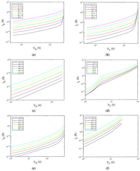
Figure 6.
Measured I−V curves at different temperatures for the three types of detectors. The left column and the right column show the reverse and forward biasing currents, respectively. (a,b) The I−V curves of D1 detector, (c,d) D2 detector, and (e,f) D3 detector.
5.2. Experimental Resistance-Voltage (Rs–V) Curves
In Figure 7 are shown the resistance Rs values vs. the bias voltage at different temperatures, obtained from the measured I–V curves (Figure 6). The Rs curves of D1 (Figure 7a,b) and D3 (Figure 7d) detectors show a well-defined maximum value at the expected voltage of Vmax = q C2/KT, in agreement with the ITD model. Therefore, the value of C2 can be easily estimated. The Vmax value, for the D2 detector, is positioned in the low voltage zone (Figure 7c) due to the prevalence of the diffusion component. Hence, the C2 value for the D2 detector cannot be estimated with this approach.
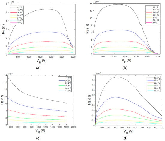
Figure 7.
Experimental resistance-voltage (Rs–V) curves at different temperatures for the three types of detectors. The Rs–V curves of D1 detector obtained from the measured (a) reverse and (b) forward currents; (c) D2 detector and (d) D3 detector.
5.3. Experimental H–V Curves
The experimental H function values versus the bias voltage are shown in Figure 8. Generally, the H–V curves follow the expected behaviour from the ITD model. The curves are quite independent on the temperature, showing decreasing values with voltage and reaching a plateau at high voltages. The H function of the D1 detector reaches a plateau between 1500–2000 V and 1400–1600 V in reverse and forward biasing, respectively. The ITD model fails at high voltages, where a marked dependence on the temperature is observed (SCLC regime). A plateau is also obtained for D2 and D3 detectors (at about 1500 V and 300 V for D2 and D3, respectively), showing a low temperature dependence.
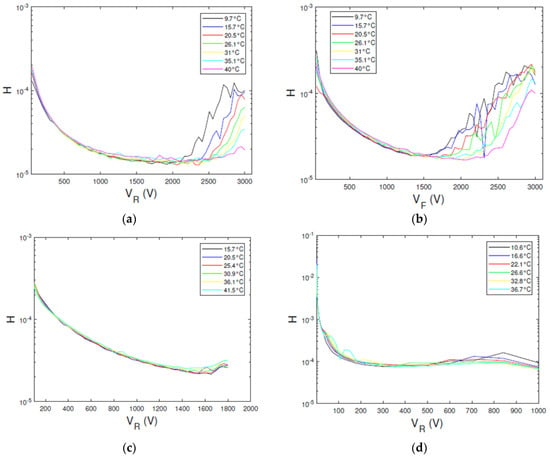
Figure 8.
Experimental H−V curves at different temperatures for the three types of detectors. The Rs−V curves of D1 detector obtained from measured (a) reverse and (b) forward currents; (c) D2 detector and (d) D3 detector.
5.4. Evaluation of Characteristic Parameters from Experimental Rs–V and H–V Curves
Table 3 summarizes the estimated C2 values obtained from the Rs–V and H–V curves. Generally, a good agreement is observed between the results of the two approaches.

Table 3.
Estimated C2 values (95% confidence interval) from the measured Rs–V and H–V curves.
Figure 9 shows the Arrhenius plots of ln(J/T2) − C2V/VTH versus q/KT, obtained at different bias voltages, properly selected in the plateau zone of the related H–V curves (Figure 8). The linear behaviour is visible, and quite good independence from the voltage is generally observed. The barrier height φB0 and the transmission coefficient θ values were calculated from the Arrhenius plots at all voltages located in the plateau zone. For each voltage, we calculated the parameter values and their errors (95% confidence interval) though a weighted linear best fitting. In Table 4 are reported the weighted mean values of the parameters over the selected voltages.
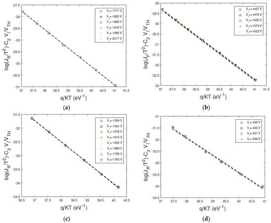
Figure 9.
Experimental Arrhenius plots of ln(J/T2) − C2V/VTH versus q/KT at different bias voltages. The voltages belong to the voltage range where the H–V curve reaches a plateau. The plots are calculated from the measured (a) reverse and (b) forward currents of D1 detector; (c) D2 detector and (d) D3 detector.

Table 4.
Estimated φB0 and θ values (95% confidence interval) from the experimental Arrhenius plots.
The reverse barrier height φB0 of the D1 detector is slightly lower than the forward one. This can explain the lower forward-leakage currents. The estimated value of the θ parameter in reverse, supposing that electrons are the majority carriers and by using a Richardson constant A* = 12 (A cm−2 K−1) (Table 1), is equal to θn = 0.36. In forward biasing, θn ≈ 1 has no physical meaning. For the D2 detector, the value of the estimated value of the effective barrier height is 0.77 eV, which is in agreement with the literature [29,30]. We obtained a transmission coefficient θn = 0.048, close to the value found in [29]. By considering the holes (with A* = 87.6 (A cm−2 K−1) [42]), we estimated a θh = 0.0004.
The Arrhenius plots, related to the D3 detector, give a barrier height of 0.74 eV, in agreement with our previous measurements by using the resistance contact approach [21]. By considering light holes involved in the transport mechanism, a θh = 0.18 was estimated.
6. Discussion and Conclusions
We presented a novel approach to evaluate the characteristic parameters of the electrical contacts of CZT and CdTe detectors. The method is based on a simple analysis of the I–V curves through the application of a new function, termed the H function. The following key results are obtained:
- (i)
- the analysis of the behaviour of H–V curves, together with the resistance–voltage curves, allows for a clear identification of the main mechanisms controlling the currents, often masked in the I–V curves;
- (ii)
- the presence of the plateau zone in the H–V curves highlights the bias voltage range where the thermionic emission dominates; this allows for the estimation of the C2 parameter characterizing the barrier lowering due to the voltage drop across the interfacial layer;
- (iii)
- the knowledge of both C2 and the current values in the TE regime is helpful for the estimation of further characteristic parameters of the electrical contacts. The slope and the intercept of the linear Arrhenius plots of ln(J/T2) − C2V/VTH give the estimation of the barrier height φB0 and the transmission coefficient θ. In this case, the correct identification of the TE voltage range and the introduction of the barrier lowering (through the parameter C2) allow for an accurate estimation of these parameters.
To strengthen the results obtained from our approach, we modelled the experimental I–V curves with the ITD model (Equation (1)) by using the parameters (θ, C2, φB0) estimated with the H function method. The results, related to the D2 detector, are shown in Figure 10. A good agreement between the data and the ITD function was obtained. The modelling at lower voltages (<1000 V) requires further details about the expression of VD (Equation (2)).
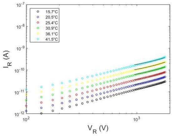
Figure 10.
Successfully ITD modelling (Equation (1); black lines) of the measured I−V curves of the D2 detector at different temperatures.
The presence of the barrier lowering can be often masked in the I–V curves, giving non-accurate estimations of the characteristic parameters of the electrical contacts. For example, we observed a dominant diffusion mechanism in the D2 detector in the investigated temperature range. In this case, the current depends on the temperature by the following relation (Equation (4)):
The barrier height is estimated by measuring the current at a range of temperatures for a fixed voltage and by fitting Equation (8) to an Arrhenius plot of the data [13]. By implementing the previous equation to the measured leakage currents of the D2 detector in the same voltage range used in the application of the H function method, we obtained the Arrhenius plots of Figure 11. We note that the intercept values depend on the reverse-bias voltage where the reverse current is measured, unlike the Arrhenius plots of Figure 9c. From the slopes of the linear fits of Figure 11 we obtained a φB0 of 0.74 ± 0.03 eV. This underestimation of the barrier height value, if compared with the value obtained with the H function method, cannot be explained by the different temperature dependence of the diffusion model (i.e., J α T 3/2) with that of the thermionic emission assumed in the implementation of the H function (i.e., J α T2). Indeed, in the investigated temperature range the change in barrier height value due to the change in the exponent of the absolute temperature is smaller than 1%. This difference is due to the lack of the barrier-lowering term C2 V/VTH in Equation (8), which causes the underestimation of the barrier height value. We stress that when the contribution of the barrier lowering in the leakage currents is small, i.e., with C2 V< VTH, the expected exponential behavior can be approximated to a linear trend, therefore masking the barrier lowering.
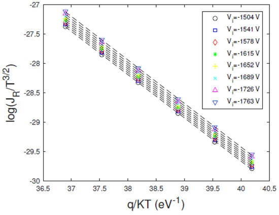
Figure 11.
Measured Arrhenius plots of ln(J/T3/2) versus q/KT at different bias voltages (D2 detector). We assumed only the diffusion mechanism governing the transport mechanism. The dashed lines are the linear fits.
Author Contributions
Conceptualization, F.P. and L.A.; formal analysis, L.A., F.P., investigation, L.A., F.P., A.Z. and M.B.; writing—original draft preparation, L.A., F.P., A.Z. and M.B.; writing—review and editing, all authors; supervision, F.P. and L.A.; project administration, F.P. and L.A.; funding acquisition, F.P. and L.A. All authors have read and agreed to the published version of the manuscript.
Funding
This work was supported by the Italian Ministry for University and Research (MUR), under AVATAR X project No. POC01_00111, by the European Union (EU) under the project—FESR o FSE, PON Ricerca e Innovazione 2014–2020—DM 1062/2021 and FFR2023.
Conflicts of Interest
The authors declare no conflict of interest.
References
- Johns, P.M.; Nino, G.C. Room temperature semiconductor detectors for nuclear security. J. Appl. Phys. 2019, 126, 040902. [Google Scholar] [CrossRef]
- Abbene, L.; Del Sordo, S. CdTe Detectors. Compr. Biomed. Phys. 2014, 8, 285–314. [Google Scholar]
- Del Sordo, S.; Abbene, L.; Caroli, E.; Mancini, A.M.; Zappettini, A.; Ubertini, P. Progress in the development of CdTe and CdZnTe semiconductor radiation detectors for astrophysical and medical applications. Sensors 2009, 9, 3491–3526. [Google Scholar] [CrossRef] [PubMed]
- Owens, A. Semiconductor materials and radiation detection. J. Synchrotron Rad. 2006, 13, 143–150. [Google Scholar] [CrossRef] [PubMed]
- Mele, F.; Quercia, J.; Abbene, L.; Benassi, G.; Bettelli, M.; Buttacavoli, A.; Principato, F.; Zappettini, A.; Bertuccio, G. Advances in High Energy Resolution CdZnTe Linear Array Pixel Detectors with Fast and Low Noise Readout Electronics. Sensors. 2023, 23, 2167. [Google Scholar] [CrossRef]
- Abbene, L.; Principato, F.; Gerardi, G.; Buttacavoli, A.; Cascio, D.; Bettelli, M.; Amadè, N.S.; Seller, P.; Veale, M.C.; Fox, O.; et al. Room-Temperature X-ray response of cadmium-zinc-Telluride pixel detectors grown by the vertical Bridgman technique. J. Synchrotron Rad. 2020, 27, 319–328. [Google Scholar] [CrossRef]
- Koch-Mehrin, K.A.L.; Bugby, S.L.; Lees, J.E.; Veale, M.C.; Wilson, M.D. Charge Sharing and Charge Loss in High-Flux Capable Pixelated CdZnTe Detectors. Sensors 2021, 21, 3260. [Google Scholar] [CrossRef]
- Meuris, A.; Limousin, O.; Lugiez, F.; Gevin, O.; Blondel, C.; Pinsard, F.; Vassal, M.C.; Soufflet, F.; Le Mer, I. Caliste 64 a new CdTe micro-camera for hard X-ray spectro-imaging. Nucl. Instr. Meth. A 2009, 610, 154–157. [Google Scholar] [CrossRef]
- Bell, S.J.; Baker, M.A.; Duarte, D.D.; Schneider, A.; Seller, P.; Sellin, P.J.; Veale, M.C.; Wilson, M.D. Characterization of the metal–semiconductor interface of gold contacts on CdZnTe formed by electroless deposition. J. Phys. D Appl. Phys. 2015, 48, 275304. [Google Scholar] [CrossRef]
- Egarievwe, S.U.; Hossain, A.; Okwechime, I.O.; Egarievwe, A.A.; Jones, D.E.; Roy, U.N.; James, R.B. Effects of Chemical Treatments on CdZnTe X-Ray and Gamma-Ray Detectors. IEEE Trans. Nucl. Sci. 2016, 63, 1091–1098. [Google Scholar] [CrossRef]
- González, R.; Pérez, J.; Vela, O.; de Burgos, E.; Oller, J.; Gostilo, V. Electrical characterization of large volume CdZnTe coplanar detectors. Nucl. Instr. Meth. A 2005, 547, 517–534. [Google Scholar] [CrossRef]
- Zha, G.; Jie, W.; Zeng, D.; Xu, Y.; Zhang, W.; Xu, F. The study on Schottky contact between Au and clean CdZnTe. Surf. Sci. 2006, 600, 2629–2632. [Google Scholar] [CrossRef]
- Bell, S.J.; Baker, M.A.; Duarte, D.D.; Schneider, A.; Seller, P.; Sellin, P.J.; Veale, M.C.; Wilson, M.D. Comparison of the surfaces and interfaces formed for sputter and electroless deposited gold contacts on CdZnTe. Appl. Surf. Sci. 2018, 427, 1257–1270. [Google Scholar] [CrossRef]
- Buttacavoli, A.; Principato, F.; Gerardi, G.; Bettelli, M.; Sarzi Amadè, N.; Zappettini, A.; Seller, P.; Veale, M.C.; Fox, O.; Sawhney, K.; et al. Room-temperature performance of 3 mm-thick cadmium zinc telluride pixel detectors with sub-millimetre pixelization. J. Synchrotron Rad. 2020, 27, 1180–1189. [Google Scholar] [CrossRef] [PubMed]
- Abbene, L.; Gerardi, G.; Raso, G.; Principato, F.; Zambelli, N.; Benassi, G.; Bettelli, M.; Zappettini, A. Development of new CdZnTe detectors for room-temperature high-flux radiation measurements. J. Synchrotron Rad. 2017, 24, 429–438. [Google Scholar] [CrossRef] [PubMed]
- Buttacavoli, A.; Principato, F.; Gerardi, G.; Cascio, D.; Raso, G.; Bettelli, M.; Zappettini, A.; Taormina, V.; Abbene, L. Window-Based Energy Selecting X-ray Imaging and Charge Sharing in Cadmium Zinc Telluride Linear Array Detectors for Contaminant Detection. Sensors 2023, 23, 3196. [Google Scholar] [CrossRef] [PubMed]
- Takahashi, T.; Paul, B.; Hirose, K.; Matsumoto, C.; Ohno, R.; Ozaki, T.; Mori, K.; Tomita, Y. High-resolution Schottky CdTe diode for hard X-ray and gamma-ray astronomy. Nucl. Instr. Meth. A 1999, 436, 111–119. [Google Scholar] [CrossRef]
- Toyama, H.; Yamazato, M.; Higa, A.; Maehama, T.; Ohno, R.; Toguchi, M. Formation of Aluminum Schottky Contact on Plasma-Treated Cadmium Telluride Surface. Jpn. J. Appl. Phys. 2004, 43, 6371–6375. [Google Scholar] [CrossRef]
- Abbene, L.; Gerardi, G.; Turturici, A.A.; Del Sordo, S.; Principato, F. Experimental results from Al/p-CdTe/PtX-ray detectors. Nucl. Instr. Meth. A 2013, 730, 135–140. [Google Scholar] [CrossRef]
- Abbene, L.; Gerardi, G.; Principato, F.; Del Sordo, S.; Raso, G. Direct measurement of mammographic X-Ray spectra with a digital CdTe detection system. Sensors 2012, 12, 8390–8404. [Google Scholar] [CrossRef]
- Principato, F.; Gerardi, G.; Abbene, L. Time-dependent current-voltage characteristics of Al/p-CdTe/Pt x-ray detectors. J. Appl. Phys. 2012, 112, 094506. [Google Scholar] [CrossRef]
- Farella, I.; Montagna, G.; Mancini, A.M.; Cola, A. Study on Instability Phenomena in CdTe Diode-Like Detectors. IEEE Trans. Nucl. Sci. 2009, 56, 1736–1742. [Google Scholar] [CrossRef]
- Thomas, B.; Veale, M.C.; Wilson, M.D.; Seller, P.; Schneider, A.; Iniewski, K. Characterisation of Redlen high-flux CdZnTe. J. Inst. 2017, 12, C12045. [Google Scholar] [CrossRef]
- Veale, M.C.; Booker, P.; Cross, S.; Hart, M.D.; Jowitt, L.; Lipp, J.; Schneider, A.; Seller, P.; Wheater, R.M.; Wilson, M.D.; et al. Characterization of the Uniformity of High-Flux CdZnTe Material. Sensors 2020, 20, 2747. [Google Scholar] [CrossRef] [PubMed]
- Abbene, L.; Gerardi, G.; Principato, F.; Bettelli, M.; Seller, P.; Veale, M.C.; Fox, O.; Sawhney, K.; Zambelli, N.; Benassi, G.; et al. Dual-polarity pulse processing and analysis for charge-loss correction in cadmium–zinc–telluride pixel detectors. J. Synchrotron Rad. 2018, 25, 1078–1092. [Google Scholar] [CrossRef]
- Buttacavoli, A.; Principato, F.; Gerardi, G.; Cascio, D.; Raso, G.; Bettelli, M.; Zappettini, A.; Seller, P.; Veale, M.C.; Abbene, L. Incomplete Charge Collection at Inter-Pixel Gap in Low-and High-Flux Cadmium Zinc Telluride Pixel Detectors. Sensors 2022, 22, 1441. [Google Scholar] [CrossRef]
- Iniewski, K. CZT sensors for Computed Tomography: From crystal growth to image quality. J. Inst. 2016, 11, C12034. [Google Scholar] [CrossRef]
- Baussens, O.; Ponchut, C.; Ruat, M.; Bettelli, M.; Zanettini, S.; Zappettini, A. Characterization of High-Flux CdZnTe with optimized electrodes for 4th generation synchrotrons. J. Inst. 2022, 17, C11008. [Google Scholar] [CrossRef]
- Bolotnikov, A.; Boggs, S.; Chen, C.H.; Cook, R.; Harrison, F.; Schindler, S. Properties of Pt Schottky type contacts on high-resistivity CdZnTe detectors. Nucl. Instr. Meth. A 2002, 482, 395–407. [Google Scholar] [CrossRef]
- Wu, C. Interfacial layer-thermionic-diffusion theory for the Schottky barrier diode. J. Appl. Phys. 1982, 53, 5947–5950. [Google Scholar] [CrossRef]
- Bettelli, M.; Amadè, N.; Zanettini, S.; Nasi, L.; Villani, M.; Abbene, L.; Principato, F.; Santi, A.; Pavesi, M.; Zappettini, A. Improved electroless platinum contacts on CdZnTe X and γ rays detectors. Sci. Rep. 2020, 10, 13762. [Google Scholar] [CrossRef] [PubMed]
- Turturici, A.; Abbene, L.; Gerardi, G.; Benassi, G.; Bettelli, M.; Calestani, D.; Zambelli, N.; Raso, G.; Zappettini, A.; Principato, F. Electrical properties of Au/CdZnTe/Au detectors grown by the boron oxide encapsulated Vertical Bridgman technique. Nucl. Instr. Meth. A 2016, 830, 243–250. [Google Scholar] [CrossRef]
- Abbene, L.; Principato, F.; Gerardi, G.; Bettelli, M.; Seller, P.; Veale, M.C.; Zappettini, A. Digital fast pulse shape and height analysis on cadmium–zinc–telluride arrays for high-flux energy-resolved X-ray imaging. J. Synchrotron Rad. 2018, 25, 257–271. [Google Scholar] [CrossRef] [PubMed]
- Chen, H.; Awadalla, S.A.; Iniewski, K.; Lu, P.H.; Harris, F.; Mackenzie, J.; Hasanen, T.; Chen, W.; Redden, R.; Bindley, G.; et al. Characterization of large cadmium zinc telluride crystals grown by traveling heater method. J. Appl. Phys. 2008, 103, 014903. [Google Scholar] [CrossRef]
- Chen, H.; Awadalla, S.A.; Mackenzie, J.; Redden, R.; Bindley, G.; Bolotnikov, A.E.; Camarda, G.S.; Carini, G.; James, R.B. Characterization of Traveling Heater Method (THM) Grown Cd0.9Zn0.1Te Crystals. IEEE Trans. Nucl. Sci. 2007, 54, 811–816. [Google Scholar] [CrossRef]
- Abbene, L.; Gerardi, G.; Principato, F.; Buttacavoli, A.; Altieri, S.; Protti, N.; Tomarchio, E.; Del Sordo, S.; Auricchio, N.; Bettelli, M.; et al. Recent advances in the development of high-resolution 3D cadmium–zinc–telluride drift strip detectors. J. Synchrotron Rad. 2020, 27, 1564–1576. [Google Scholar] [CrossRef]
- Abbene, L.; Principato, F.; Buttacavoli, A.; Gerardi, G.; Bettelli, M.; Zappettini, A.; Altieri, S.; Auricchio, N.; Caroli, E.; Zanettini, S.; et al. Potentialities of high-resolution 3-D CZT drift strip detectors for prompt gamma-ray measurements in BNCT. Sensors 2022, 22, 1502. [Google Scholar] [CrossRef]
- Kuvvetli, I.; Budtz-Jørgensen, C.; Caroli, E.; Auricchio, N. CZT drift strip detectors for high energy astrophysics. Nucl. Instr. Meth. A 2010, 624, 486–491. [Google Scholar] [CrossRef]
- Sammartini, M.; Gandola, M.; Mele, F.; Garavelli, B.; Macera, D.; Pozzi, P.; Bertuccio, G. A CdTe pixel detector–CMOS preamplifier for room temperature high sensitivity and energy resolution X and γ ray spectroscopic imaging. Nucl. Instr. Meth. A 2018, 910, 168–173. [Google Scholar] [CrossRef]
- Abbene, L.; Gerardi, G.; Principato, F. Digital performance improvements of a CdTe pixel detector for high flux energy-resolved X-ray imaging. Nucl. Instr. Meth. A 2015, 777, 54–62. [Google Scholar] [CrossRef]
- Turturici, A.; Abbene, L.; Gerardi, G.; Principato, F. Electrical characterization of CdTe pixel detectors with Al Schottky anode. Nucl. Instr. Meth. A 2014, 763, 476–482. [Google Scholar] [CrossRef]
- Prokesch, M.; Szeles, C. Accurate measurement of electrical bulk resistivity and surface leakage of CdZnTe radiation detector crystals. J. Appl. Phys. 2006, 100, 014503. [Google Scholar] [CrossRef]
Disclaimer/Publisher’s Note: The statements, opinions and data contained in all publications are solely those of the individual author(s) and contributor(s) and not of MDPI and/or the editor(s). MDPI and/or the editor(s) disclaim responsibility for any injury to people or property resulting from any ideas, methods, instructions or products referred to in the content. |
© 2023 by the authors. Licensee MDPI, Basel, Switzerland. This article is an open access article distributed under the terms and conditions of the Creative Commons Attribution (CC BY) license (https://creativecommons.org/licenses/by/4.0/).