
An Indoor-Monitoring LiDAR Sensor for Patients with Alzheimer Disease Residing in Long-Term Care Facilities


 and
and 
Abstract
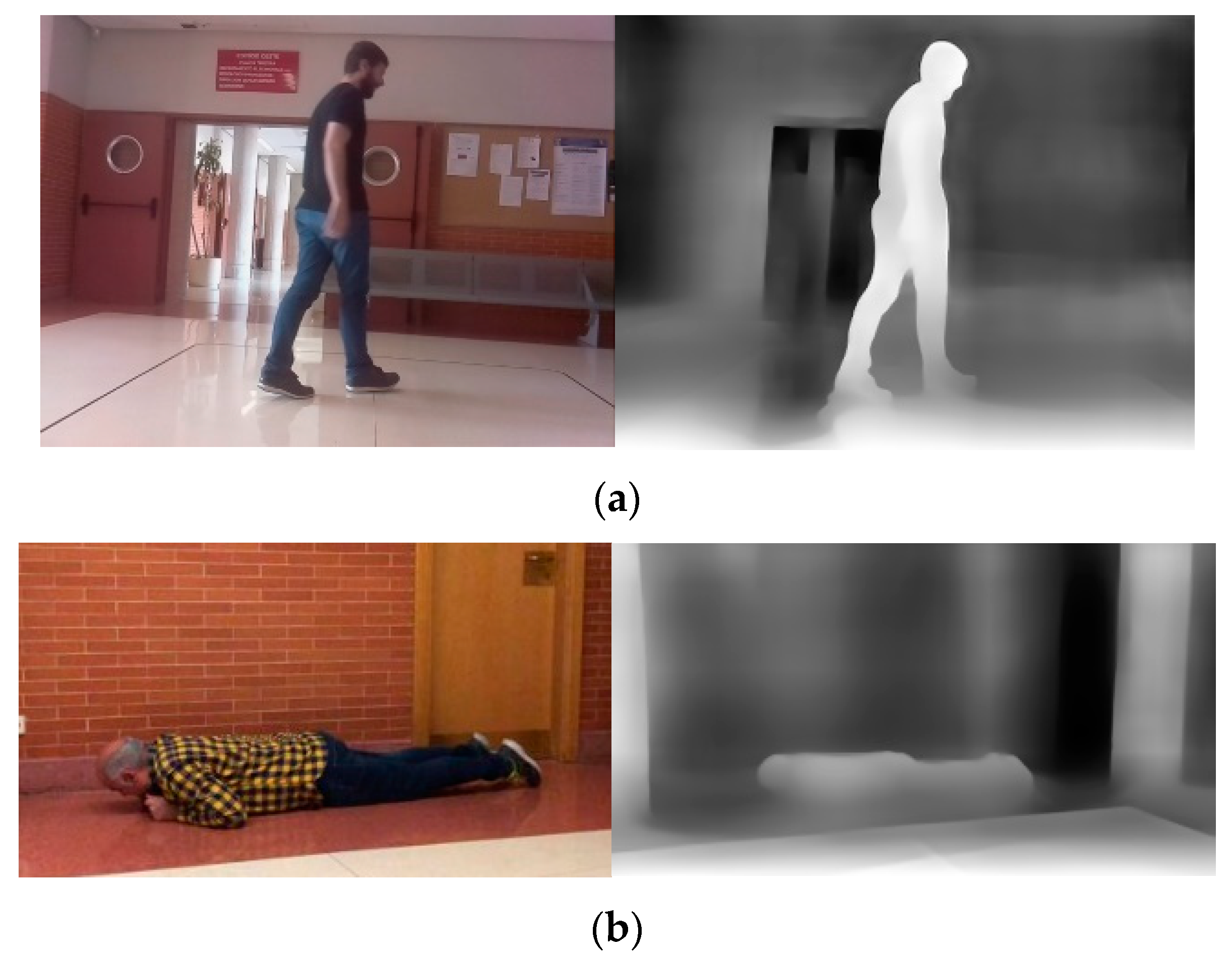
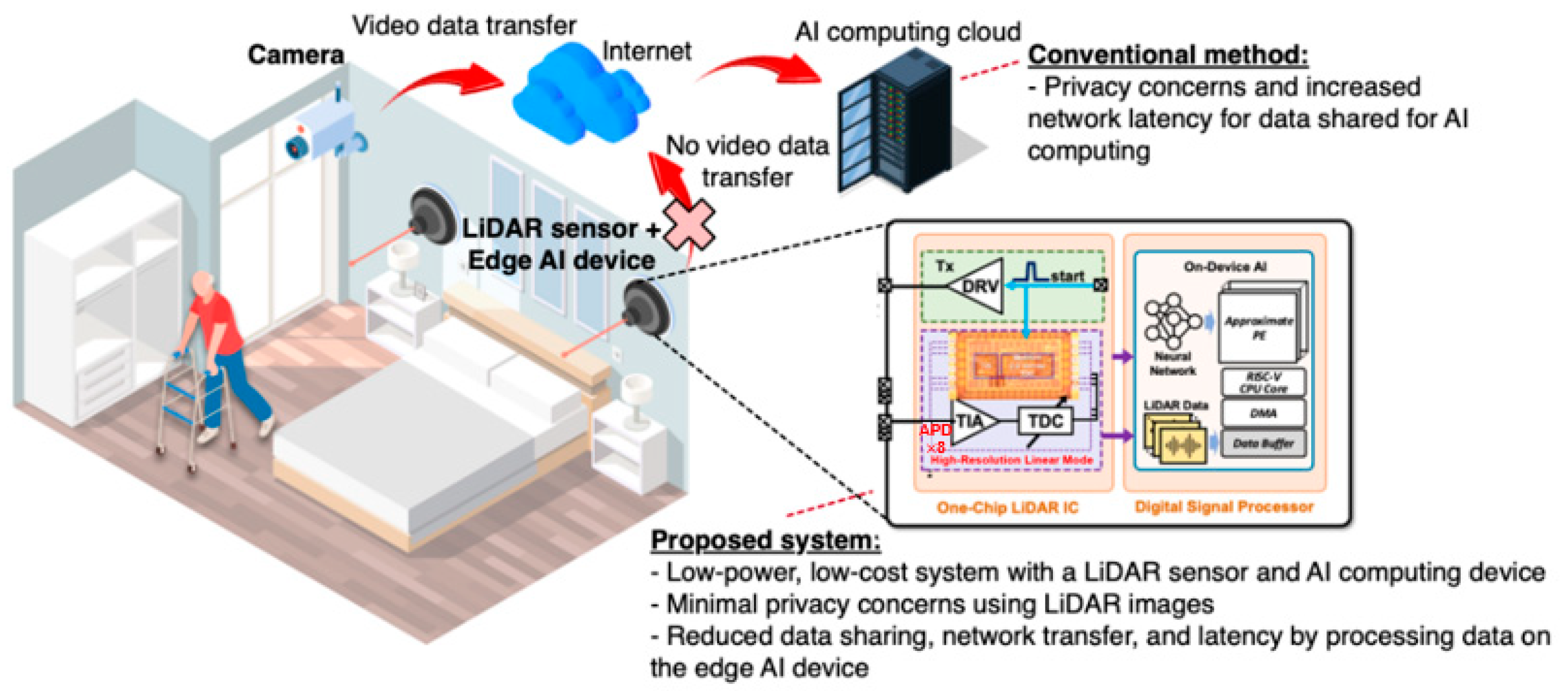
1. Introduction
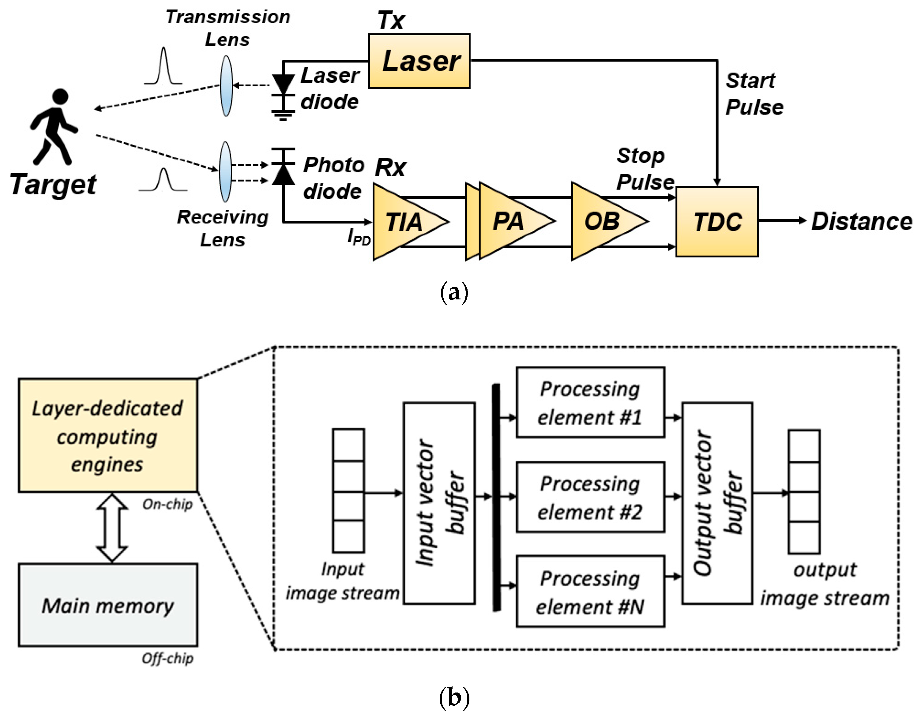
2. LiDAR AFE
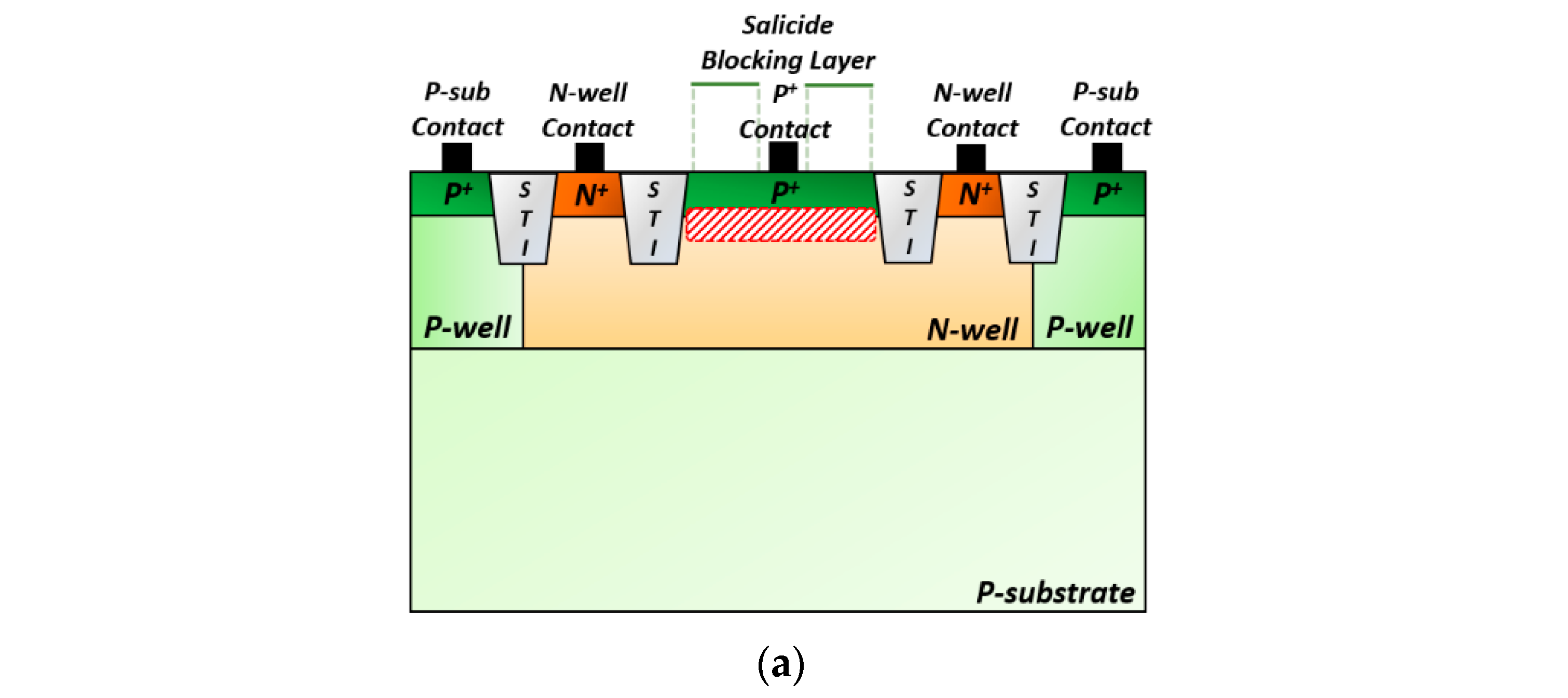
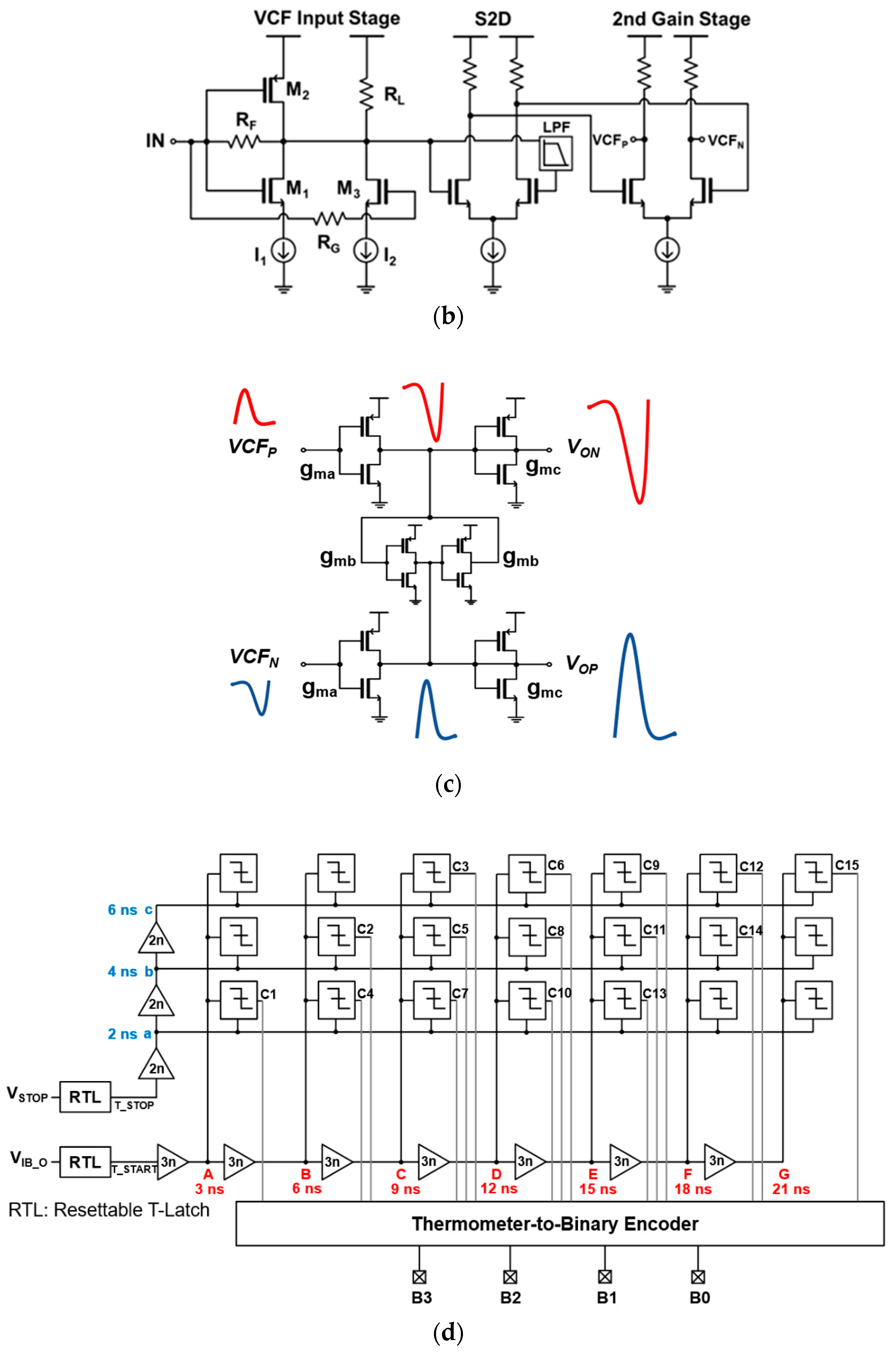
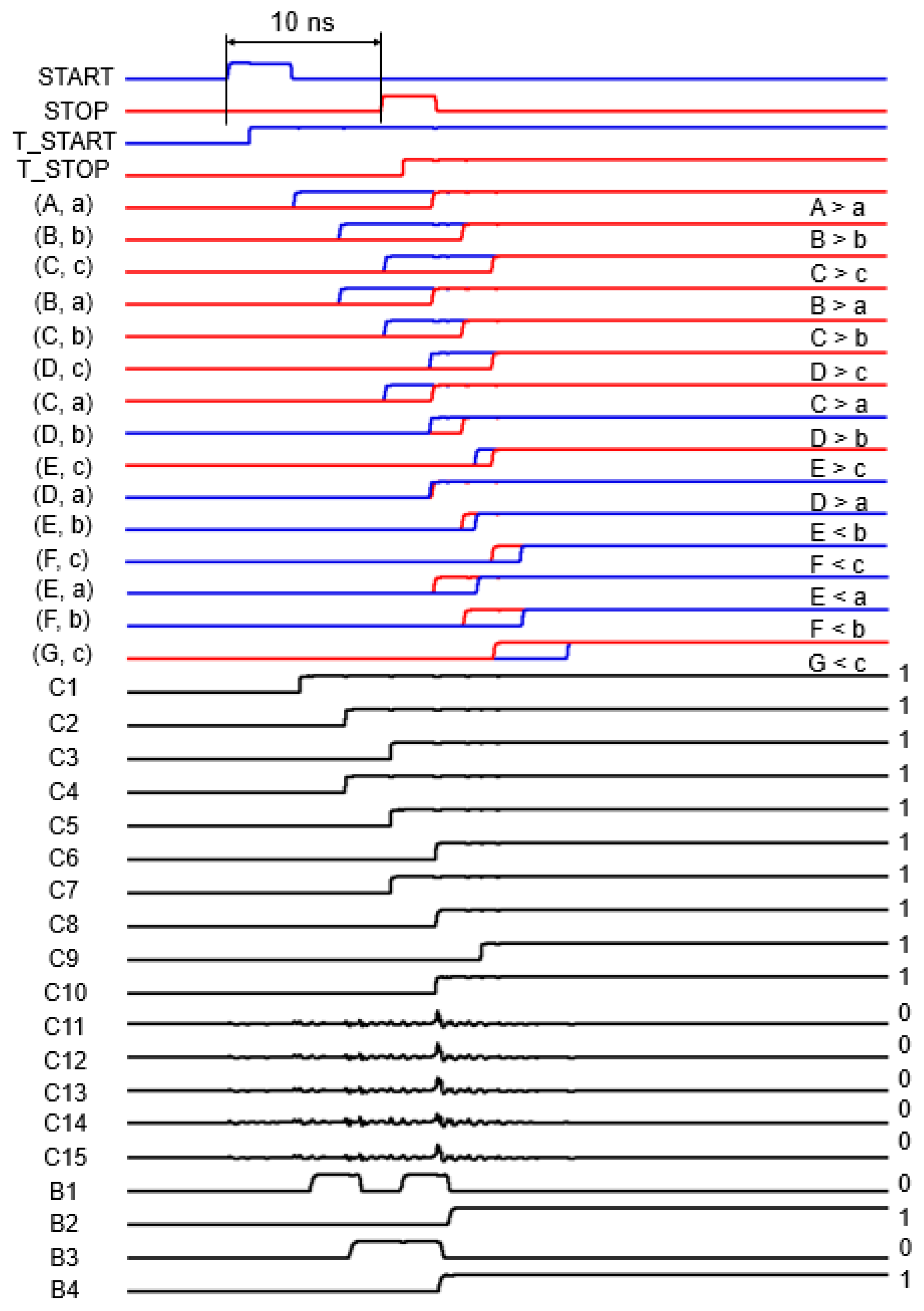
2.1. Circuit Description
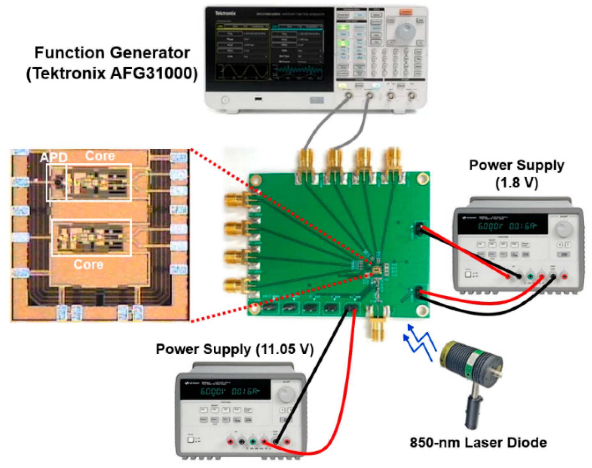
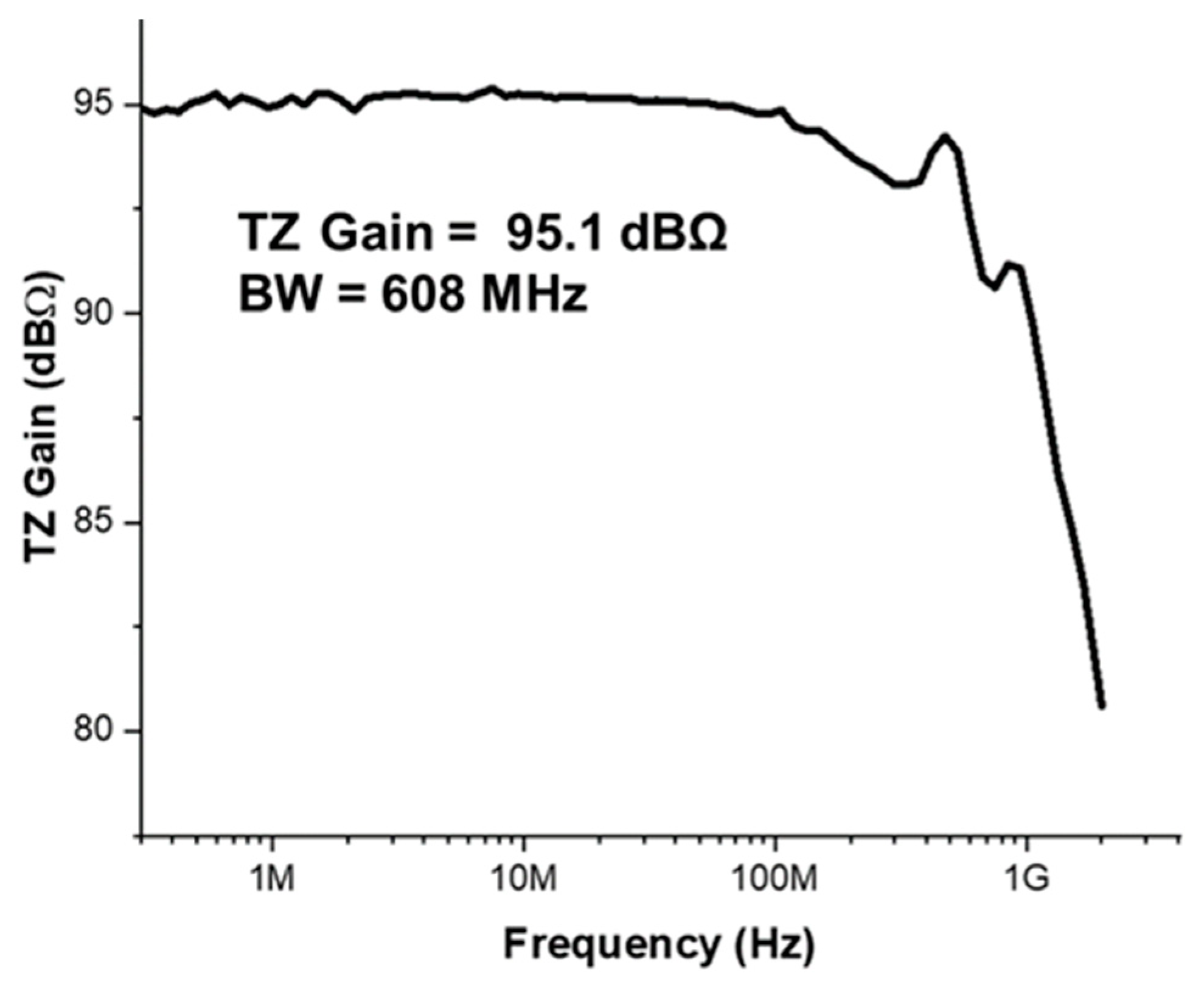
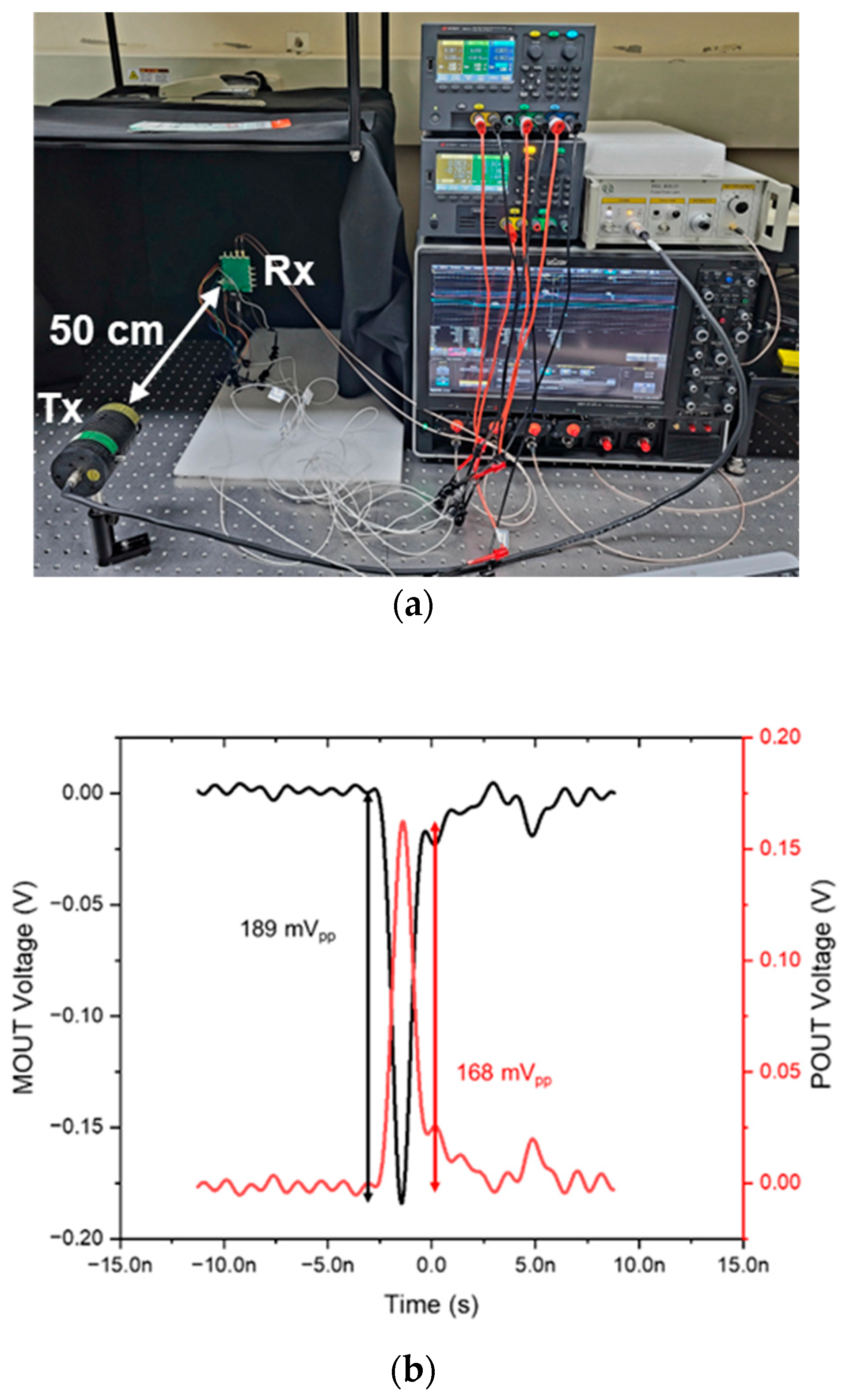
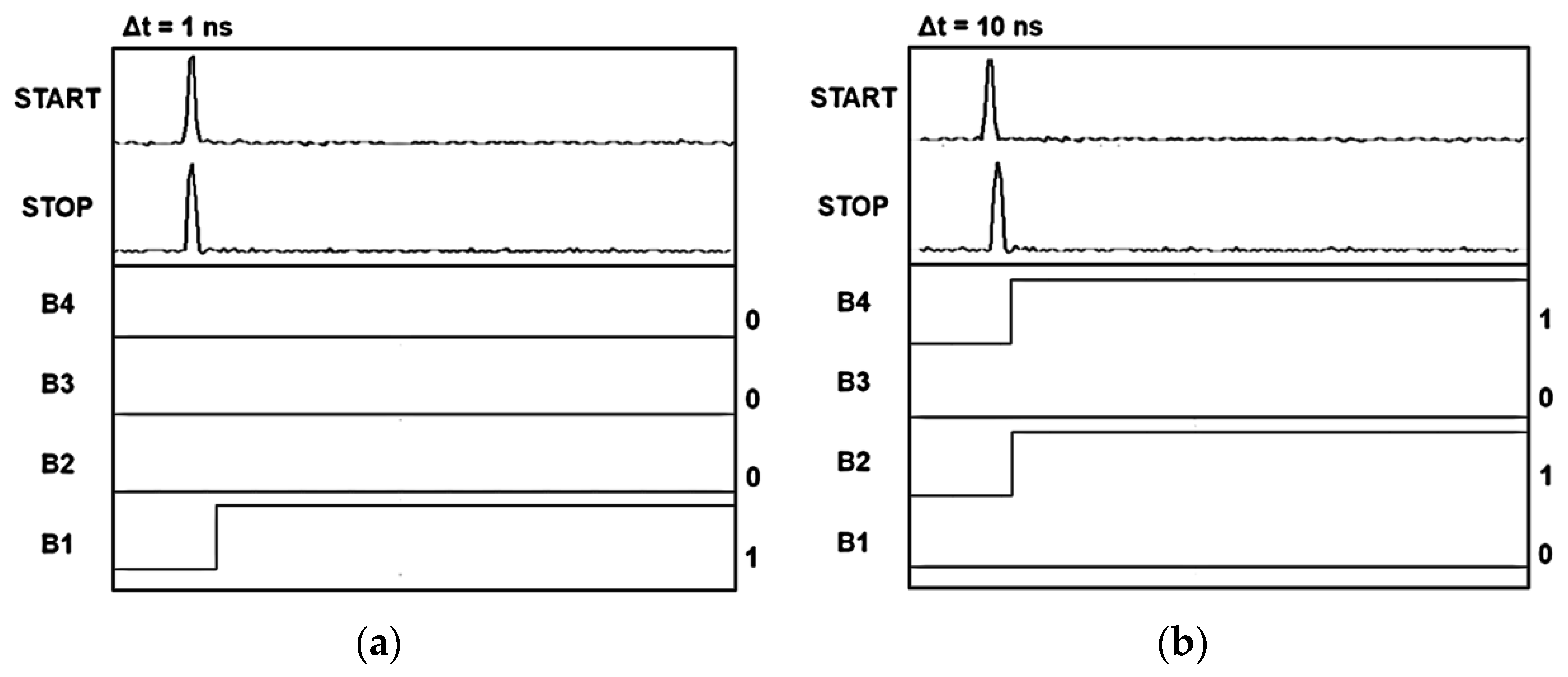
2.2. Measured Results
3. Neural Processing Unit
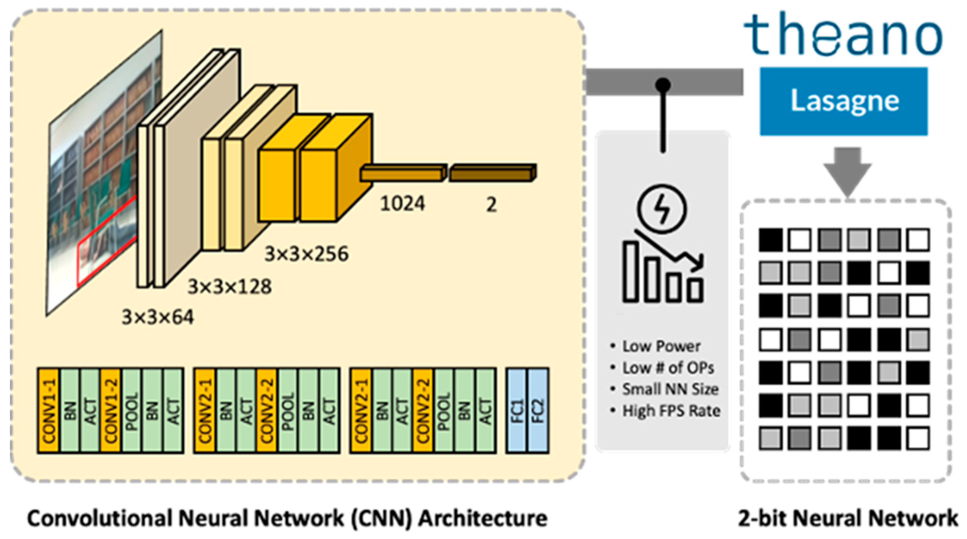
3.1. Quantized CNN Model
3.2. Design Flow and Toolchain
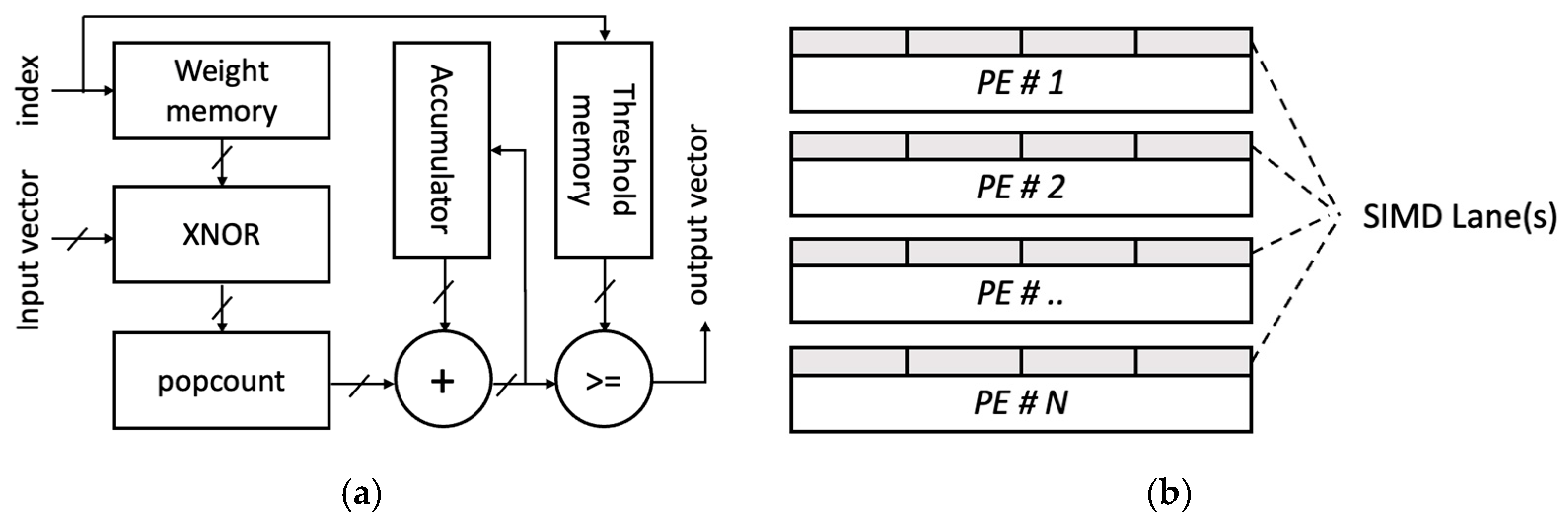
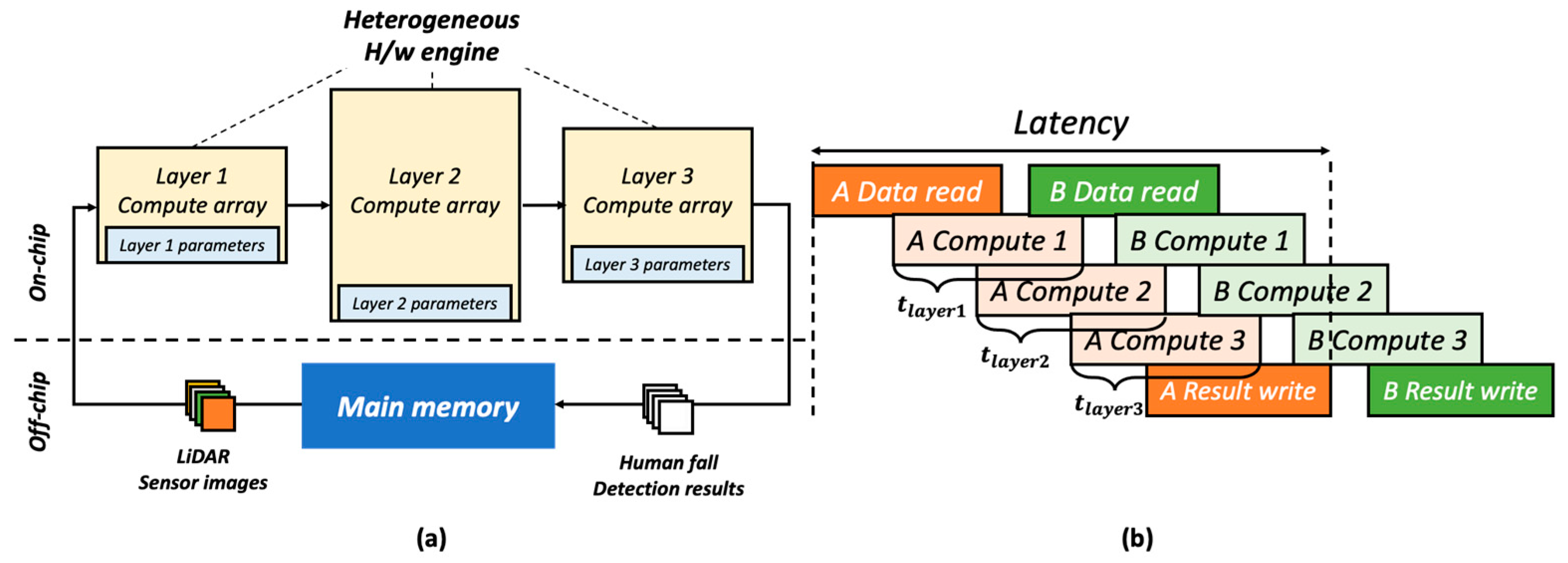
3.3. Hardware Architecture
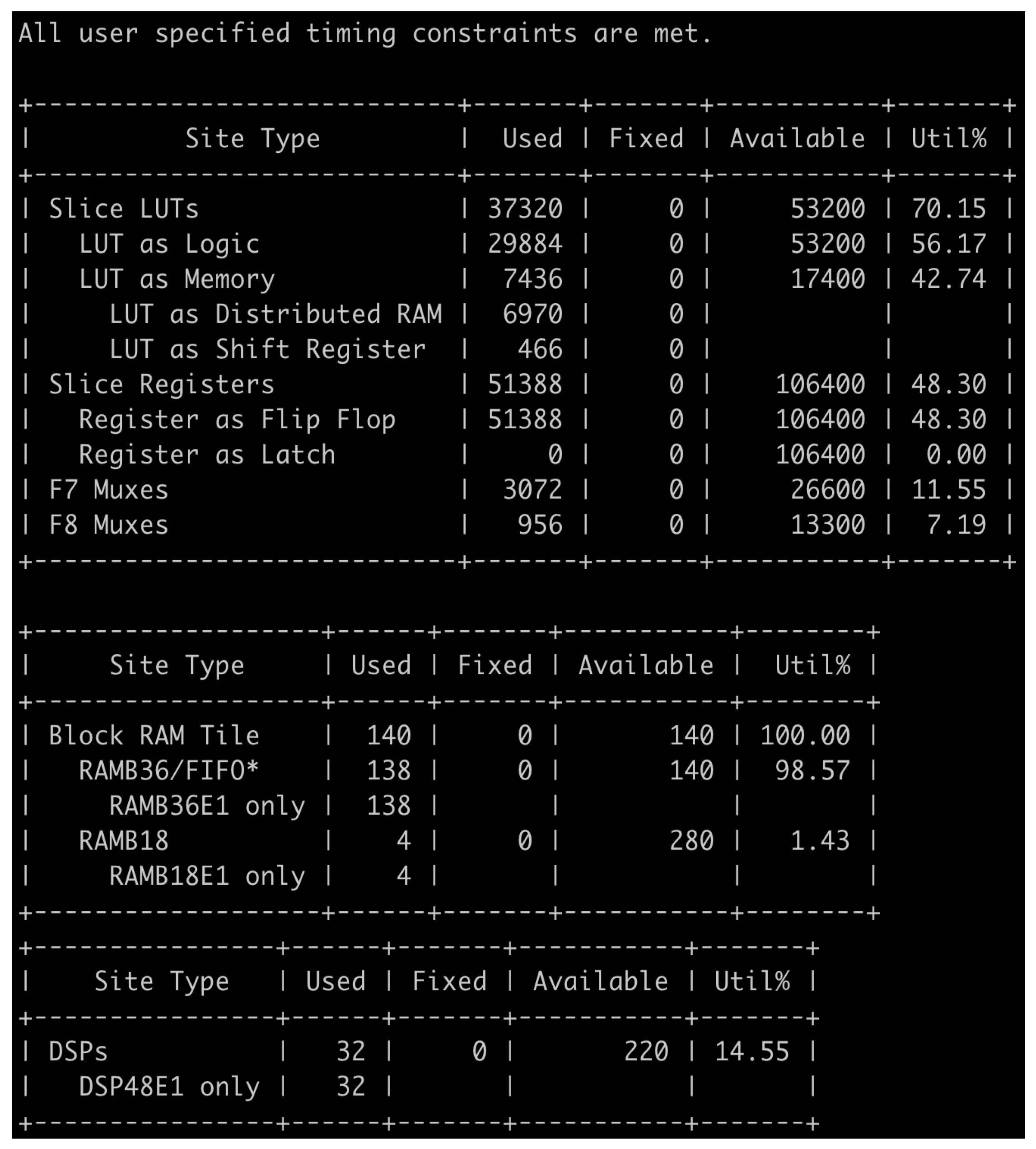
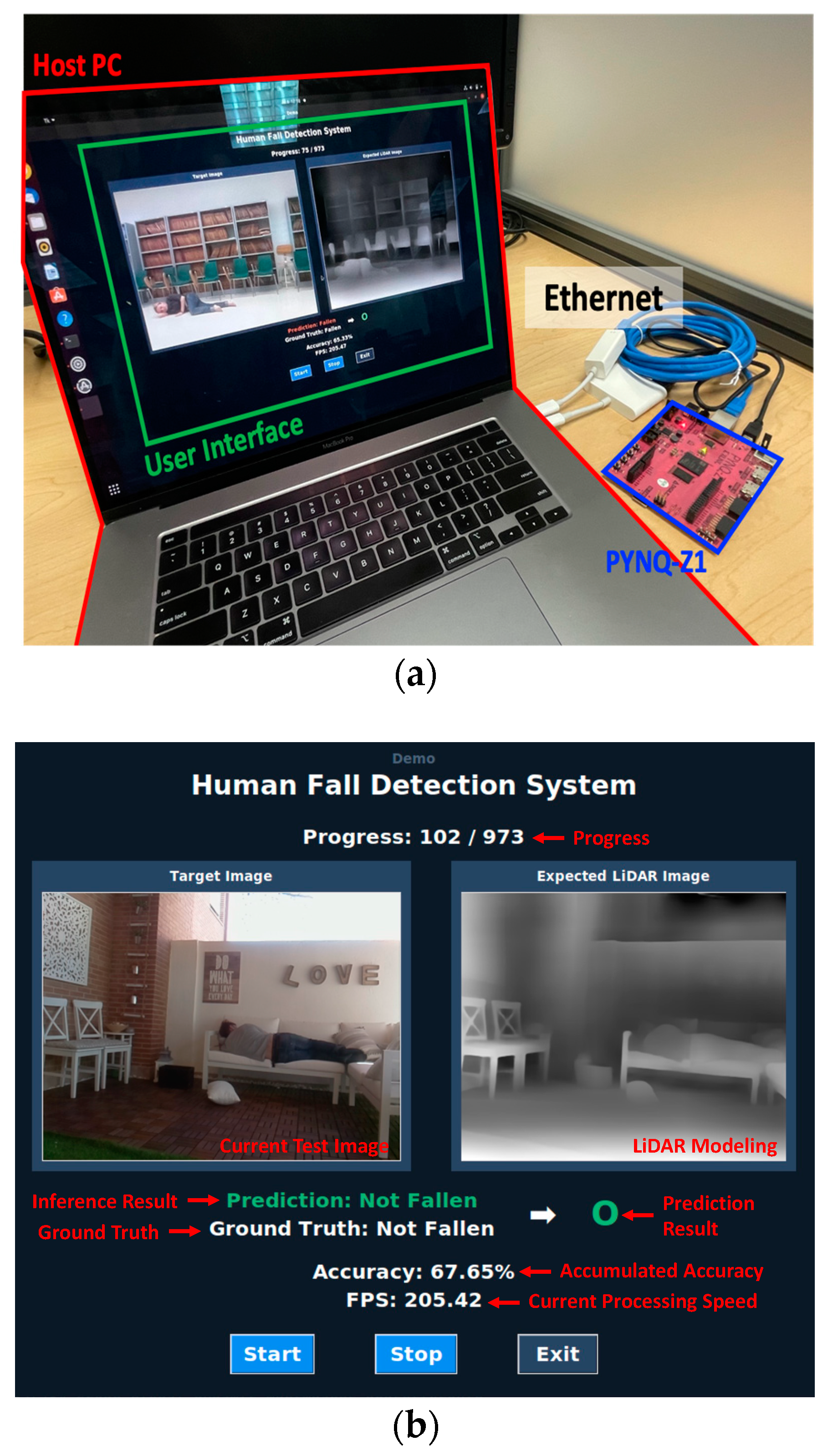
3.4. Evaluation
4. Conclusions
Author Contributions
Funding
Institutional Review Board Statement
Informed Consent Statement
Acknowledgments
Conflicts of Interest
References
- Yoon, D.S.; Joo, J.E.; Park, S.M. Mirrored current-conveyor transimpedance amplifier for home minotoring LiDAR sensors. IEEE Sensors J. 2020, 20, 5589–5597. [Google Scholar]
- Joo, J.; Lee, M.-J.; Park, S.M. A CMOS optoelectronic receiver IC with an on-chip APD for home-monitoring LiDAR sensors. Sensors 2021, 21, 4364. [Google Scholar] [CrossRef] [PubMed]
- Hong, C.; Kim, S.-H.; Kim, J.-H.; Park, S.M. A Linear-Mode LiDAR Sensor Using a Multi-Channel CMOS Transimpedance Amplifier Array. IEEE Sensors J. 2018, 18, 7032–7040. [Google Scholar] [CrossRef]
- Chen, J.; Kwong, K.; Chang, D.; Luk, J.; Bajcsy, R. Wearable Sensors for Reliable Fall Detection. In Proceedings of the 2005 IEEE Engineering in Medicine and Biology 27th Annual Conference, Shanghai, China, 17–18 January 2006; pp. 3551–3554. [Google Scholar]
- Tan, X.; Ai, B. The issues of cloud computing security in high-speed railway. In Proceedings of the 2011 International Conference on Electronic & Mechanical Engineering and Information Technology, Harbin, China, 12–14 August 2011; pp. 4358–4363. [Google Scholar]
- An, S.; Ogras, U.Y. MARS: MmWave-Based Assistive Rehabilitation System for Smart Healthcare. ACM Trans. Embed. Comput. Syst. 2021, 20, 1–22. [Google Scholar] [CrossRef]
- Kashima, K.; Nakamura, R.; Kajiwara, A. Bathroom Movements Monitoring UWB Sensor with Feature Extraction Algorithm. In Proceedings of the 2013 IEEE Sensors Applications Symposium Proceedings, Galveston, TX, USA, 19–21 February 2013; pp. 118–122. [Google Scholar]
- Tepencelik, O.N.; Wei, W.; Chukoskie, L.; Cosman, P.C.; Dey, S. Body and Head Orientation Estimation with Privacy Preserving LiDAR Sensors. In Proceedings of the 29th European Signal Processing Conference (EUSIPCO), Dublin, Ireland, 23–27 August 2021; pp. 766–770. [Google Scholar]
- Günter, A.; Böker, S.; König, M.; Hoffmann, M. Privacy-preserving People Detection Enabled by Solid State LiDAR. In Proceedings of the 16th International Conference on Intelligent Environments (IE), Madrid, Spain, 20–23 July 2020; pp. 1–4. [Google Scholar]
- Maldonado-Bascón, S.; Iglesias, C.; Martin, P.; Lafuente-Arroyo, S. Fallen People Detection Capabilities Using Assistive Robot. Electronics 2019, 8, 915. [Google Scholar] [CrossRef]
- Ranftl, R.; Lasinger, K.; Hafner, D.; Schindler, K.; Koltun, V. Towards Robust Monocular Depth Estimation: Mixing Datasets for Zero-Shot Cross-Dataset Transfer. IEEE Trans. Pattern Anal. Mach. Intell. 2022, 44, 1623–1637. [Google Scholar] [CrossRef] [PubMed]
- Jang, Y.M.; He, Y.; Cho, S.B.; Kim, J.-H.; Park, S.M. A Modified 2-D Vernier Time-to-digital Converter Using Resettable T-latch. J. Semicond. Tech. Sci. 2019, 19, 477–484. [Google Scholar] [CrossRef]
- Kurtti, S.; Kostamovaara, J. A CMOS Receiver-TDC Chip Set for Accurate Pulsed TOF Laser Ranging. IEEE Trans. Instrum. Meas. 2020, 69, 2208–2217. [Google Scholar] [CrossRef]
- Wang, X.; Ma, R.; Li, D.; Zheng, H.; Liu, M.; Zhu, Z. A low walk error analog front-end circuit with intensity compensation for direct ToF LiDAR. IEEE Trans. Circuits Syst. I 2020, 67, 4309–4321. [Google Scholar] [CrossRef]
- Jocher, G.; Ma, R.; Liu, M.; Zhu, Z. Ultralytics/yolov5: v6.1—TensorRT, TensorFlow Edge TPU and OpenVINO Export and Inference (v6.1). 2022. Available online: https://zenodo.org/record/6222936#.Y00p7UxByUk (accessed on 22 February 2022). [CrossRef]
- Rami, A. Theano: A Python framework for fast computation of mathematical expressions. arXiv 2016, arXiv:1605.02688. [Google Scholar]
- Dieleman, S. Lasagne: First Release. 2015. Available online: https://zenodo.org/record/27878#.Y00owkxByUk (accessed on 13 August 2015).
- Available online: http://www.pynq.io/ (accessed on 1 May 2022).
- Available online: https://github.com/Xilinx/BNN-PYNQ (accessed on 1 May 2022).
- Umuroglu, Y. Finn: A framework for fast, scalable binarized neural network inference. In Proceedings of the 2017 ACM/SIGDA International Symposium on Field-Programmable Gate Arrays, Monterey, CA, USA, 22–24 February 2017; pp. 65–74. [Google Scholar]
- Available online: https://github.com/Xilinx/finn-hlslib (accessed on 1 May 2022).
- Available online: https://www.xilinx.com/ (accessed on 20 May 2022).
- Samajdar, A.; Zhu, Y.; Whatmough, P.; Mattina, M.; Krishna, T. SCALE-Sim: Systolic CNN Accelerator Simulator. arXiv 2019, arXiv:1811.02883. [Google Scholar]


| Parameters | This Work | [2] | [3] | [10] | [12] | |
|---|---|---|---|---|---|---|
| CMOS technology (nm) | 180 | 180 | 180 | 350 | 180 | |
| PD | Type | APD (on-chip) | APD (on-chip) | InGaAs PIN-PD (off-chip) | APD (off-chip) | APD (off-chip) |
| Cpd (pF) | 0.5 | 0.5 * | 0.5 | 3.0 | 1.2 | |
| Responsivity (A/W) | 2.72 | 2.72 | 0.9 | 40 | 50 | |
| Wavelength (nm) | 850 | 850 | 1550 | 905 | 905 | |
| TZ gain (dBΩ) | 95.1 | 93.4 | 76.3 | 100 | 86 | |
| Bandwidth (MHz) | 608 | 790 | 720 | 230 | 281 | |
| Noise current spectral density (pA/√Hz) | 4.54 | 12 | 6.3 | 6.32 | 4.68 | |
| Detection range (m) | 10 † | 10 | 25 | 34 | N/A | |
| Power dissipation (mW) | 51.5 | 56.5 | 29.8 | 180 | 200 | |
| Conv1 | Conv2 | Maxpool | Conv3 | Conv4 | Maxpool | Conv5 | Conv6 | FC | FC | FC | |
|---|---|---|---|---|---|---|---|---|---|---|---|
| PE | 16 | 32 | - | 16 | 16 | - | 4 | 1 | 1 | 1 | 4 |
| SIMD | 3 | 32 | - | 32 | 32 | - | 32 | 32 | 4 | 8 | 1 |
Publisher’s Note: MDPI stays neutral with regard to jurisdictional claims in published maps and institutional affiliations. |
© 2022 by the authors. Licensee MDPI, Basel, Switzerland. This article is an open access article distributed under the terms and conditions of the Creative Commons Attribution (CC BY) license (https://creativecommons.org/licenses/by/4.0/).
Share and Cite
Joo, J.-E.; Hu, Y.; Kim, S.; Kim, H.; Park, S.; Kim, J.-H.; Kim, Y.; Park, S.-M. An Indoor-Monitoring LiDAR Sensor for Patients with Alzheimer Disease Residing in Long-Term Care Facilities. Sensors 2022, 22, 7934. https://doi.org/10.3390/s22207934
Joo J-E, Hu Y, Kim S, Kim H, Park S, Kim J-H, Kim Y, Park S-M. An Indoor-Monitoring LiDAR Sensor for Patients with Alzheimer Disease Residing in Long-Term Care Facilities. Sensors. 2022; 22(20):7934. https://doi.org/10.3390/s22207934
Chicago/Turabian StyleJoo, Ji-Eun, Yu Hu, Sujin Kim, Hyunji Kim, Sunyoung Park, Ji-Hoon Kim, Younghyun Kim, and Sung-Min Park. 2022. "An Indoor-Monitoring LiDAR Sensor for Patients with Alzheimer Disease Residing in Long-Term Care Facilities" Sensors 22, no. 20: 7934. https://doi.org/10.3390/s22207934
APA StyleJoo, J.-E., Hu, Y., Kim, S., Kim, H., Park, S., Kim, J.-H., Kim, Y., & Park, S.-M. (2022). An Indoor-Monitoring LiDAR Sensor for Patients with Alzheimer Disease Residing in Long-Term Care Facilities. Sensors, 22(20), 7934. https://doi.org/10.3390/s22207934