Abstract
In this paper, we have numerically investigated a metasurface based perfect absorber design, established on the impedance matching phenomena. The paper comprises of two parts. In the first part, the device performance of the perfect absorber—which is composed of silicon nano-cylindrical meta-atoms, periodically arranged on a thin gold layer—is studied. The device design is unique and works for both x-oriented and y-oriented polarized light, in addition to being independent of the angle of incidence. In the second part of the paper, a CO2 gas sensing application is explored by depositing a thin layer of functional host material—a polyhexamethylene biguanide polymer—on the metasurface. The refractive index of the host material decreases due to the absorption of the CO2 gas. As a result, the resonance wavelength of the perfect absorber performs a prominent blueshift. With the help of the proposed sensor design, based on metasurface, the CO2 gas concentration range of 0–524 ppm was detected. A maximum sensitivity of 17.3 pm/ppm was acquired for a gas concentration of 434 ppm. The study presented in this work explores the opportunity of utilizing the metasurface perfect absorber for gas sensing applications by employing functional host materials.
1. Introduction
Metamaterials are artificial structures with permittivity and permeability levels that are unachievable in nature. They have gathered a great deal of attention due to their incredible electromagnetic (EM) response. For this reason, metamaterials are considered to have valuable prospective uses in photonics. The EM properties of materials can be modified to acquire preferred optical properties by engineering the metamaterials. In recent years, metamaterial based EM absorbers have been widely researched [1,2,3], which has demonstrated their potential usage in solar photovoltaic and thermophotovoltaic devices [4], spatial light modulation [5] and sensing applications [6]. Based on the range of light spectrum absorbed by the EM absorber, it can be categorized into two types: a narrowband EM absorber [7] and a broadband EM absorber [8]. Typically, the dimensions of the metasurfaces are far beyond the wavelength, which substitutes the need for bulk optics and they are therefore capable of nanoscale light manipulation [9,10].
Several recent studies on perfect absorbers (PAs), such as the metacavity model with multilayer metasurfaces [11], electromagnetically induced absorption [12], subwavelength hole arrays [13,14] and structured metal surfaces [15] have demonstrated perfect absorption phenomena. For practical purposes, PAs that are insensitive to polarization and the incident angle of light are typically desirable [16]. These PAs can be employed in sensing applications based on the wavelength interrogation method.
For studying global warming and other environmental-related problems triggered by anthropogenic greenhouse gas discharge, the accurate measurement of carbon dioxide (CO2) gas concentrations in the atmosphere is essential. Considering that the existing level of ambient CO2 gas concentration is swiftly reaching the 400 ppm threshold, which is far above the 350 ppm threshold to prevent inevitable climate change [17], there is a growing need for miniaturized and precise CO2 gas sensors that can be proficiently used in large-area sensor networks to track greenhouse gas concentration patterns. In health sciences, there is also a strong interest in CO2 gas monitoring, as it reveals an essential role in several biological activities. Non-dispersive infrared spectroscopy (NDIR) is established on the recognition of the signature absorption band of CO2 at the 4.26 μm wavelength and is currently the prevailing CO2 sensing technology. There are two main sensor configurations which can be used to detect the toxic gases such as evanescent field gas absorption [18,19,20] and the resonance wavelength interrogation method [21,22].
A photonic CO2 gas sensor based on infrared evanescent field absorption is presented here, which is capable of detecting CO2 concentrations down to 5000 ppm [23]. This level is associated with headaches, sleepiness, loss of attention, increased heart rate and slight nausea. Other notable studies on integrated photonic gas sensors based on evanescent field absorption can be found here [24,25,26,27]. The refractive index gas sensor is another widely used method, where a shift in resonance wavelength is observed for the increasing gas concentration. Recently, an attractive design for a CO2 gas sensor based on subwavelength grating (SWG) slot waveguide has been numerically proposed, which offers the best sensitivity of 12.9 pm/ppm [28]. However, practically, it requires a great deal of effort to directly couple the light into the slot waveguide. It requires an additional ridge to slot waveguide, converted to transform the fundamental dielectric mode to the slot waveguide mode [29]. For readers’ interest, we have mentioned some notable gas sensors based on the resonance wavelength interrogation method [30,31,32,33]. In our previous studies [29,34,35,36,37], we have presented distinctive designs for gas sensors based on optical waveguides working on an evanescent field absorption mechanism. Here, we propose an attractive arrangement for a metasurface formed by a periodic array of silicon nano-cylindrical meta-atoms (MAs) deposited on a metal layer. This configuration offers the possibility to be employed as a narrowband PA. Moreover, when the metasurface is coated with a specific thin layer of a functional host material, it can function as a gas sensor. The sensor design proposed in this work is numerically investigated; we are unable to provide the experimental results to show the repeatability of the device due to the limited research activities during the COVID-19 pandemic. However, in [38], the repeatability of the sensor system employing the same functional layer was confirmed by performing 10 repeated cycles of measurements, with each cycle consisting of applying 50 ppm CO2 gas flow, measuring the resonance shift and purging the chamber with N2 gas. Their analysis showed that the repeatability of the sensor is ±20 ppm.
2. Device Design and Theory
Metamaterials can be described by a complex electric permittivity and magnetic permeability and , respectively. The main concern, however, was on the real part of permittivity () and permeability () for fabricating negative refractive index materials [39]. However, the loss of components of the optical constants ( and ) are anticipated in order to create a variety of practical uses such as Pas, which can be employed as filters and sensors. By regulating the resonances in ε and µ independently, it is conceivable to absorb both the incident electric and magnetic field. This kind of absorber exhibits tremendous merits over its conventional predecessors due to its compact size and extraordinary features. The key perception is to reduce the reflectance by impedance matching and concurrently discarding the transmittance by magnifying the metamaterial losses. In this work, we explored two potential applications of metasurface such as narrowband PA and CO2 gas detection by utilizing a host functional polymer layer polyhexamethylene biguanide (PHMB) deposited on top of the metasurface.
2.1. Narrowband PA Design
The schematic of the proposed metasurface based narrowband PA design is presented in Figure 1. It is composed of a periodic array of silicon nano-cylindrical MAs placed on a gold (Au) layer deposited on a quartz substrate. The inset shows the zoomed image of silicon cylindrical MAs of radius R placed on the Au layer. Moreover, the general transmission, reflection and absorption spectrum is also shown. The height of the silicon cylindrical MAs and the Au is denoted as HSi and HAu, respectively. The HAu was fixed at 100 nm throughout the paper, which is bigger than the skin depth, therefore, it was modelled as a perfect electric conductor (PEC). Thus, the EM wave does not penetrate in the near-IR range and the transmission is nearly null. The gap between the two MAs is represented as 2d where d is the gap between MA and the boundary.
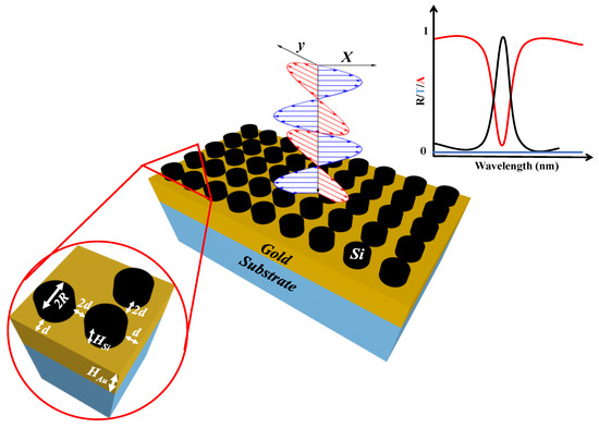
Figure 1.
Schematic of a narrowband perfect absorber (PA) based on a silicon nano-cylinder metasurface. Inset shows the silicon MAs periodically arranged on the gold layer (left-bottom). The transmission, reflection and absorption spectrum is also shown (right-top).
The transmission, reflection, absorption and electric-field distribution of the proposed device are calculated by utilizing the finite element method (FEM), based on a commercially available COMSOL Multiphysics software. By considering a single unit cell, the additional simulation volume is avoided which leads to a reduced simulation time [40]. On four sides of the unit cell, Floquet-periodic boundary conditions are applied to mimic the unbounded 2D array. Due to the periodic boundary condition (PBC) applied on the lateral sides of the design, the distance between two MAs is automatically doubled, i.e., 2d. The refractive index (n = 1.0) is filled in the domains above and below the absorber design, which represents the air medium. The proposed absorber configuration is positioned between the source port and the output port. The source port emits the EM waves which are analyzed at the output port. Port boundary conditions are positioned on the inner boundaries of the perfect matched layers (PMLs), adjoining to the air domains which establish the transmission and reflection features in terms of S-parameters. Where S11 and S21 are the reflection and transmission coefficient that can be written as:
where
L is the effective length, is the effective refractive index, and are the effective permittivity and permeability. Γ is the reflection coefficient which can be calculated as:
where Zo is the relative impedance.
The inner port boundaries with the PML backing require the slit condition. For the calculation of S-parameter, the port direction is set to classify the inward direction. Since we are not interested in the higher-order diffraction modes, the combination of domain-backed type slit ports and PMLs are utilized in place of a diffraction order port for each diffraction order and polarization. The PMLs are employed to absorb the excited mode from the source port and any higher-order modes produced by the periodic structures. The PMLs diminish the EM wave propagating in the direction perpendicular to the PML boundary.
2.2. Silicon Nano-Cylinder Metasurface Coated with PHMB Polymer Layer for CO2 Gas Detection
CO2 is a colorless, odorless and non-flammable greenhouse gas typically generated by the combustion of carbonaceous materials or by the metabolism of animals [41]. The current CO2 gas concentration and its growth rate is leading to global warming and unsustainable environmental challenges [42]. For that reason, high sensitivity CO2 gas sensors have been widely researched to track patterns in the concentrations of greenhouse gases. As the concentration of the CO2 gas in the ambient medium increases, the refractive index of functionalization layers changes. PHMB has basic amide-bearing functional groups and is a member of the guanidine polymer family [43]. It is an ideal contender for a functionalization polymer layer that is equally sensitive and selective to low concentrations of CO2 at room temperature and atmospheric pressure. Additionally, the absorption and release of CO2 gas from the material does not require water vapor to be applied, as is the case with the previously reported functional materials [44]. The resonance wavelength blueshift of gas sensors based on the functional material of PHMB, is linearly interrelated to the CO2 concentration [28,38,45]. To the best of our knowledge, we have not witnessed any reports claiming that gases other than CO2 can interfere with the sensitivity of the PHMB polymer layer. For this reason, it is possible to utilize such a polymer layer for the realization of the CO2 gas sensor. In [38], the author analyzed the selectivity of PHMB as a functional layer for CO2 gas against hydrogen gas. Being the smallest gas molecule, hydrogen voluntarily penetrates and diffuses into many polymeric materials, so it is imperative to confirm that the H2 gas does not induce an undesirable refractive index change in the PHMB layer and cause the false detection of CO2. It was demonstrated that the sensor showed no response to H2 or N2 gas and only reacted to the presence of CO2 gas. The schematic of the gas sensor is shown in Figure 2a and the inset shows the reflection spectrum in the absence and presence of CO2 gas. Moreover, the chemical formula for CO2 gas adsorption and release is shown in Figure 2b [43]. The modification of the refractive index of the PHMB layer can be expounded in terms of the redistribution of the electron density of the polymer repeating units due to the binding of the CO2 molecules, which results in variation in its polarizability.
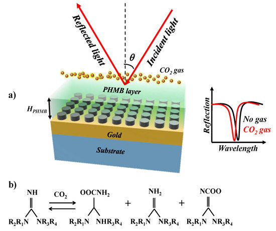
Figure 2.
(a) A thin layer of PHMB functional layer is deposited on the metasurface. This scheme is used to detect the CO2 gas via wavelength interrogation method, (b) Reaction between CO2 gas and amide-bearing functional groups.
The sensing mechanism is based on the wavelength interrogation method of the reflected light. The absorption offered by the proposed metasurface is tolerant to the angle of incidence of light (AOI) which will be demonstrated later in the paper. The broadband light is used to excite the sample at 45 °C which absorbs a certain wavelength when the impedance matching condition is fulfilled. The reflected light is collected with the help of a photodetector which is used to convert the photons into current and is examined via a spectrum analyzer. When the CO2 gas is injected in the chamber, it is absorbed by the PHMB layer. As a result, the refractive index of the layer decreases which translates the λres to a lower wavelength. The change in the refractive index of the PHMB layer, as well as the wavelength shift, is dependent on the concentration of the gas.
3. Optimization of Narrowband PA Design
In this section, we optimized the performance of the PA structure by varying the geometric parameters of the device, such as R, HSi and d. The maximum absorption is attained when ε and µ satisfy the impedance-matched condition, i.e., ε(ω) = µ(ω), at the operational wavelength [46]. The absorption is calculated by using the following expression:
where transmission ≈ 0, due to the thick gold layer deposited on the substrate. Therefore, the absorption is directly dependent on the reflection.
Absorption (A) = 1 − Transmission (T) − Reflection (R)
3.1. Variation in R at Constant Remaining Parameters
The resonance wavelength (λres) and absorption of the device are calculated for different values of R while maintaining other geometric parameters at a constant value such as HSi = 50 nm, d = 300 nm and HAu = 100 nm. R is varied between 100 nm and 250 nm with a step size of 25 nm. The spectral characteristic of the device is plotted for the near-infrared region with the help of built-in “parametric sweep” function where the wavelength is incremented with a step size of 0.5 nm. From Figure 3a, it can be seen that λres can be tuned between 821 nm to 1024 nm as R is increased from 100 nm to 250 nm. The maximum absorption of 0.92 is obtained at R = 200 nm at λres = 982 nm. However, we are adopting R = 150 nm for further investigation which also provides an absorption (A = 0.905) close to the absorption obtained when R = 200 nm. The selection is based on the smooth line shape of the spectrum and the small footprint of the device. However, the absorption can be further enhanced by depositing the PHMB layer on the metasurface as explained afterwards in the paper.
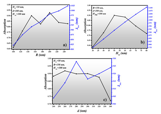
Figure 3.
Spectral characteristics of the metasurface absorber, (a) Radius of meta-atoms (MA) versus absorption and resonance wavelength, (b) Height of MA versus absorption and resonance wavelength, (c) Gap between MA versus absorption and resonance wavelength.
3.2. Variation in HSi at Constant Remaining Parameters
After optimizing the R of the MAs, the next thing is to improve the height of the MAs placed on the gold layer. For that reason, we have varied HSi between 30 nm to 80 nm with a step size of 10 nm by keeping R, d and HAu fixed at 150 nm, 300 nm and 100 nm, respectively. Figure 3b presents λres and the absorption plotted versus HSi. It is worth noting that λres shows the same trend as HSi increases. So, we can tune the wavelength of the absorbing light either by manipulating R or HSi. The absorption capability of the MAs increases as HSi is varied from 30 nm to 50 nm. However, when HSi is further increased, the absorption potential of the device decreases. This is due to the mismatch in the ε and µ at the operational wavelength.
3.3. Variation in d at Constant Remaining Parameters
In Section 3.1 and Section 3.2, the optimized values of R and HSi are achieved at 150 nm and 50 nm, where the absorption is 0.905. Here, we have optimized the gap between two MAs, i.e., 2d. Figure 3c presents the absorption and λres plot versus d which is varied between 240 nm to 340 nm with a step size of 20 nm. The maximum absorption of 0.9188 is obtained at λres = 914 nm where d = 260 nm and it deteriorates as d increases. Hence, from Figure 3c, it can be predicted that the gap between two MAs should be maintained at 520 nm to preserve the absorption of 0.92.
3.4. R/T/A Plot and AOI of X-Oriented and Y-Oriented Field
The reflection, transmission and absorption spectrum is plotted for both x-oriented and y-oriented EM waves at the optimized device parameters where R = 150 nm, his = 50 nm, HAu = 100 nm and d = 260 nm as shown in Figure 4a. The λres for the x-oriented field is 914 nm where absorption is 0.9188 whereas the λres for the y-oriented field is 913.5 nm where absorption is 0.9488. This specifies that the PA is polarization-insensitive and can be employed as a narrowband filter. Furthermore, the absorption potential of the device concerning the AOI of x-oriented and y-oriented field is investigated. The absorption is retained at 0.9188 and 0.9488 for x-oriented and y-oriented polarized light for the AOI ranging between −75 degrees and +75 degrees, respectively, as shown in Figure 4b.
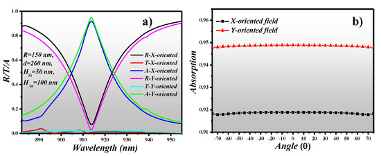
Figure 4.
(a) Transmission, reflection and absorption spectrum, (b) angle of incidence of light (AOI) of X-oriented and Y-oriented field versus absorption.
Additionally, the E-field and H-field distributions at λres for the x-oriented and y-oriented EM fields are shown in Figure 5. The 2D electric field distribution plot is taken on the surface of the MA. There is a slight difference between the λres of x-oriented and y-oriented light as can be seen in Figure 5a,b. The cross-sectional view of the E-field distribution and H-field distribution at λres = 914 nm for x-oriented light is shown in Figure 5c,d, respectively. It is worth noting that the E-field is stronger on top and inside the MA at λres, while the H-field is stronger between the MA and metal interface. The perfect matching of the E-field dipole and H-field dipole results in the eradication of the reflectance and delivers maximum absorption.
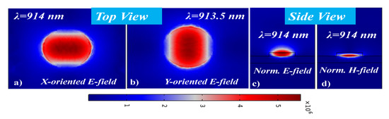
Figure 5.
Electric field distribution in MA, (a) X-oriented E-field distribution on the top of the MA at λres, (b) Y-oriented E-field distribution on the top of the MA at λres, (c) Side view of E-field distribution at λres, (d) Side view of H-field distribution at λres.
4. CO2 Gas Sensing Based on Wavelength Interrogation Method
The PA can be employed in the detection of CO2 gas by depositing a thin layer of PHMB on the surface of the metasurface. In Figure 6, we investigated the dependence of absorption and λres on HPHMB which is varied between 75 nm to 225 nm with a step size of 25 nm. The remaining geometric parameters of the device are as follows: R = 150 nm, d = 260 nm, HSi = 50 nm and HAu = 100 nm which are optimized in Section 3 for best performance. From Figure 6a, it can be seen that λres performs a redshift as HPHMB increases while a significant enhancement in absorption is also observed. The PHMB layer forms a cladding layer on the silicon MAs which helps in the confinement of the resonant light. The maximum absorption of 0.96336 is obtained at λres = 985 nm when HPHMB = 100 nm is deposited on the surface of the MAs. The R/T/A graph is plotted for the optimized device parameters in the wavelength range of 960 nm to 1015 nm, as shown in Figure 6b.
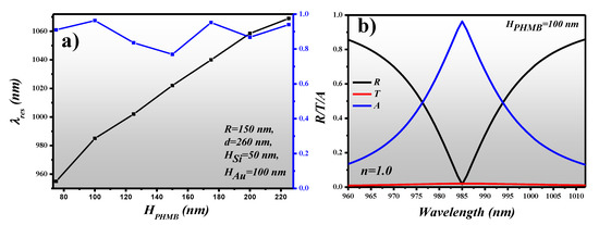
Figure 6.
(a) Absorption and λres dependence on HPHMB, (b) R/T/A plot of a polyhexamethylene biguanide (PHMB) coated PA. Here the PHMB is optimized at 100 nm. The geometric parameters of the design are R = 150 nm, d = 260 nm, HSi = 50 nm, HAu = 100 nm and HPHMB = 100 nm.
Mi et al. [38] reported a silicon ring resonator CO2 gas sensor with a PHMB functional layer deposited over the waveguide structure. By utilizing such a method, a gas concentration in the range of 0–500 ppm can be detected. The sensitivity offered by the sensor is 6 × 10⁻⁹ RIU/ppm with a detection limit of 20 ppm. In [47], a silicon dual-gas sensor realized on a wavelength-multiplexed ring resonator array for the concurrent detection of H2 and CO2 gases is proposed. In [43], an experimental study based on a PHMB based Fabry–Perot interferometric optical fiber sensor for the detection of CO2 gas is conducted. The suggested sensor model offers a sensitivity of 12.2 pm/ppm for a gas range of 0–700 ppm. Moreover, it is also concluded from the previous literature [38,43,45], that moisture does not play a role in influencing the sensitivity of the device. In [48], the authors replicated the ring resonator design proposed in [38] and carried out the numerical investigation and derived the refractive index of the PHMB layer dependence on the CO2 gas concentration, as tabulated in Table 1. From the table, it is convenient to extract the refractive index values of the PHMB layer at specific gas concentrations as well as the shift in the resonance wavelength.

Table 1.
The refractive index of the PHMB layer versus gas concentration [48].
In the absence of CO2 gas, the refractive index of the PHMB layer is ~1.55 @1000 nm which is obtained by extrapolating the data using a Cauchy model fit [44]. The reflection spectrum at different CO2 gas concentrations is plotted at 45 degrees AOI for the wavelength range of 940 nm to 1020 nm. From Figure 7, it can be seen that λres = 985 nm is obtained in the absence of the CO2 gas. However, when the concentration of gas increases, λres performs a visible blueshift. In this work, the gas detection range of 0–524 ppm was investigated.
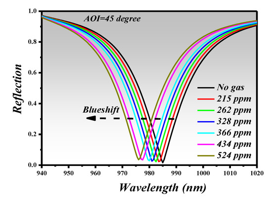
Figure 7.
Reflection spectrum versus different CO2 gas concentration in ppm.
The cross-sectional view of the E-field distribution in the silicon MA is plotted for the on-resonance and off-resonance wavelength, as shown in Figure 8a,b, respectively. At λres = 985 nm, there is a perfect matching of the E-field dipole and H-field dipole which results in the suppression of the reflectance and provides a maximum absorption while at λ = 1020 nm which is the off-resonance wavelength, the light is reflected from the surface resulting in an insignificant absorption.
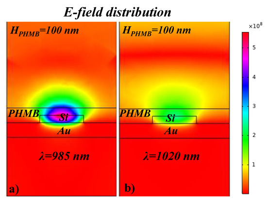
Figure 8.
A cross-sectional view of the E-field distribution in the silicon MA at, (a) on-resonance wavelength, (b) off-resonance wavelength.
From Figure 7, we extracted the spectral characteristics and tabulated them in Table 2, such as λres and ∆λres versus gas concentration. As in previous work [38,43,47], the λres is given in pm, which is why we have also converted the wavelength from nm to pm so that the spectral characteristics can be fairly related. By comparing the λres shift based on ring resonator sensor (Table 1), the proposed metasurface based PA shows a higher shift which can assist in a higher sensitivity. Moreover, from the data points obtained from [48], we can fairly say that the limit of detection (LOD) of the sensor is around 215 ppm.
Table 2.
Resonance wavelength shift versus gas concentration of the proposed sensor design.
For practical application in the detection of a small concentrations of CO2 gas, optical sensors with high sensitivity are desired. Sensitivity is the measure of the resonant wavelength shift concerning the gas concentration and is expressed as:
where ∆λ is the change in resonance wavelength (pm) and ∆conc. is the change in gas concentration (ppm). We have plotted the λres shift versus the CO2 gas concentration and found out that λres decreases as the gas concentration increases, as shown in Figure 9a. Moreover, it has a linear correlation to the CO2 gas for the given 0–524 ppm concentration. This range is of interest for atmospheric CO2 gas monitoring. Figure 9b presents the sensitivity of the proposed sensor design for the gas concentration of 0 ppm to 524 ppm. A maximum sensitivity of 17.3 pm/ppm was obtained for gas concentrations higher than 400 ppm. However, for the gas concentration < 400 ppm, the concentration is still higher than the ones reported in [28,38,42,45].
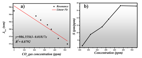
Figure 9.
(a) Resonance wavelength (nm) versus CO2 gas concentration (ppm), (b) Sensitivity (pm/ppm) versus gas concentration (ppm).
5. Anticipated Manufacturing Process
The proposed sensor device can be manufactured by the execution of the following steps, as shown in Figure 10. A thin chromium layer (5 nm–10 nm) is coated on the glass substrate, followed by thermal evaporation or electron beam (E-beam) evaporation of the gold layer. Chromium can be used to increase the gold adhesion on the substrate. Afterwards, an optimized layer thickness of silicon is deposited on the gold layer by utilizing chemical vapor deposition. E-beam lithography can be directly used to transfer the MA patterns on the electron-sensitive film known as a resist. The E-beam modifies the solubility of the resist, enabling the selective removal of the non-exposed regions of the resist by immersing it in a developer. The sample is then etched with the help of an appropriate dry etch method to form patterns of Si layers creating cylindrical MAs. In the last step, the PHMB polymer can be deposited on the metasurface by spin-coating. The thickness of the PHMB layer can be regulated by changing the spin speed, in addition to the solution concentration.
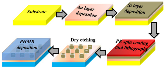
Figure 10.
Proposed fabrication step of the CO2 gas sensor.
6. Conclusions
In conclusion, a metasurface based perfect absorber is designed and numerically investigated via the finite element method. The metasurface is composed of silicon nano-cylindrical meta-atoms, periodically arranged on a gold layer. Due to the impedance matching of the electric-field dipole and the magnetic-field dipole, the maximum absorption is obtained at the resonance wavelength. The absorption of >0.9 was obtained which is independent of the polarization and angle of incidence of the light. Moreover, the gas sensing characteristics of the metasurface based absorber were explored by depositing a functional host material. For the detection of CO2 gas, polyhexamethylene biguanide (PHMB) polymer was employed, which is capable of absorbing CO2 gas. The modification in the refractive index of PHMB layer can be explained in terms of a redistribution of the electron density of the polymer repeating units due to the binding of the CO2 molecules resulting in a variation in its polarizability. The proposed gas sensor is capable of detecting CO2 gas within a concentration range of 0–524 ppm with a maximum sensitivity of 17.3 pm/ppm. The proposed sensor configuration can be utilized for the detection of other toxic gases by utilizing suitable functional host materials.
Author Contributions
Conceptualization, M.A.B. and S.N.K.; methodology, M.A.B.; software, M.A.B.; validation, N.L.K., S.N.K. and M.A.B.; formal analysis, S.N.K.; investigation, M.A.B.; resources, N.L.K.; data curation, M.A.B.; writing—original draft preparation, M.A.B.; writing—review and editing, S.N.K. and M.A.B.; visualization, N.L.K.; supervision, N.L.K.; project administration, N.L.K.; funding acquisition, N.L.K. All authors have read and agreed to the published version of the manuscript.
Funding
This work was financially supported by the Ministry of Science and Higher Education within the State assignment FSRC «Crystallography and Photonics» RAS (No. 007-GZ/Ch3363/26) for numerical calculations and Russian Science Foundation (No. 20-69-47110) for theoretical results.
Institutional Review Board Statement
Not applicable.
Informed Consent Statement
Not applicable.
Data Availability Statement
No new data were created or analyzed in this study. Data sharing is not applicable to this article.
Acknowledgments
We acknowledge the fruitful discussion with the technical staff of the department of the Technical Cybernetics, Samara National Research University, Russia.
Conflicts of Interest
The authors declare no conflict of interest.
References
- Alaee, R.; Albooyeh, M.; Rockstuhl, C. Theory of metasurface based perfect absorbers. J. Phys. D Appl. Phys. 2017, 50, 503002. [Google Scholar] [CrossRef]
- Rhee, J.Y.; Kim, Y.J.; Yi, C.; Hwang, J.S.; Lee, Y.P. Recent progress in perfect absorbers by utilizing metamaterials. J. Electromagn. Waves Appl. 2020, 34, 1338–1371. [Google Scholar] [CrossRef]
- Zhao, L.; Liu, H.; He, Z.; Dong, S. Design of multi-narrowband metamaterial perfect absorbers in near-infrared band based on resonators asymmetric method and modified resonators stacked method. Opt. Commun. 2018, 420, 95–103. [Google Scholar] [CrossRef]
- Rafangura, P.; Sabah, C. Dual-band perfect metamaterial absorber for solar cell applications. Vacuum 2015, 120, 68–74. [Google Scholar] [CrossRef]
- Savo, S.; Shrekenhamer, D.; Padilla, W.J. Liquid crystal metamaterial absorber spatial light modulator for THz applications. Adv. Opt. Mater. 2014, 2, 275–279. [Google Scholar] [CrossRef]
- Rifat, A.A.; Rahmani, M.; Xu, L.; Miroshnichenko, A.E. Hybrid metasurface based tunable near-perfect absorber and plasmonic sensor. Materials 2018, 11, 1091. [Google Scholar] [CrossRef]
- Mavrakakis, K.; Booske, J.H.; Behdad, N. Narrowband, infrared absorbing metasurface using polystyrene thin films. J. Appl. Phys. 2020, 127, 074504. [Google Scholar] [CrossRef]
- Katrodiya, D.; Jani, C.; Sorathiya, V.; Patel, S.K. Metasurface based broadband solar absorber. Opt. Mater. 2019, 89, 34–41. [Google Scholar] [CrossRef]
- Aoni, R.A.; Rahmani, M.; Xu, L.; Kamali, K.Z.; Komar, A.; Yan, J.; Neshev, D.; Miroshnichenko, A.E. High-efficiency visible light manipulation using dielectric metasurfaces. Sci. Rep. 2019, 9, 6510. [Google Scholar] [CrossRef]
- Wang, J. Metasurfaces enabling structured light manipulation: Advances and perspectives. Chin. Opt. Lett. 2018, 16, 050006. [Google Scholar] [CrossRef]
- Bhattarai, K.; Silva, S.; Song, K.; Urbas, A.; Lee, S.J.; Ku, Z.; Zhou, J. Metamaterial perfect absorber analyzed by a metacavity model consisting of multilayer metasurfaces. Sci. Rep. 2017, 7, 10569. [Google Scholar] [CrossRef] [PubMed]
- He, J.; Ding, P.; Wang, J.; Fan, C.; Liang, E. Ultra-narrow band perfect absorbers based on plasmonic analog of electromagnetically induced absorption. Opt. Express 2015, 23, 6083–6091. [Google Scholar] [CrossRef] [PubMed]
- Dao, T.D.; Ishii, S.; Yokoyama, T.; Sawada, T.; Sugavaneshwar, R.P.; Chen, K.; Wada, Y.; Nabatame, T.; Nagao, T. Hole array perfect absorbers for spectrally selective midwavelength infrared pyroelectric detectors. ACS Photonics 2016, 3, 1271–1278. [Google Scholar] [CrossRef]
- Wang, Y.; Ma, X.; Li, X.; Pu, M.; Luo, X. Perfect electromagnetic and sound absorption via subwavelength holes array. Opto-Electron. Adv. 2018, 1, 180013. [Google Scholar] [CrossRef]
- Xiong, X.; Jiang, S.-C.; Hu, Y.-H.; Peng, R.-W.; Wang, M. Structured metal film as a perfect absorber. Adv. Mater. 2013, 25, 3994–4000. [Google Scholar] [CrossRef] [PubMed]
- Butt, M.A.; Kazanskiy, N.L. Narrowband perfect metasurface absorber based on impedance matching. Photonics Lett. Pol. 2020, 12, 88–90. [Google Scholar]
- Hansen, J.; Sato, M.; Kharecha, P.; Beerling, D.; Berner, R.; Masson-Delmotte, V.; Pagani, M.; Raymo, M.; Royer, D.L.; Zachos, J.C. Target atmospheric CO2: Where should humanity aim? Open Atmos. Sci. J. 2008, 2, 217–231. [Google Scholar] [CrossRef]
- Stewart, G.; Jin, W.; Culshaw, B. Prospects for fibre-optic evanescent-field gas sensors using absorption in the near infrared. Sens. Actuators B Chem. 1997, 38, 42–47. [Google Scholar] [CrossRef]
- Butt, M.A.; Degtyarev, S.A.; Khonina, S.N.; Kazanskiy, N.L. An evanescent field absorption gas sensor at mid-IR 3.39 μm wavelength. J. Mod. Opt. 2017, 64, 1892–1897. [Google Scholar] [CrossRef]
- Kazanskiy, N.L.; Khonina, S.N.; Butt, M.A. Polarization-Insensitive hybrid plasmonic waveguide design for evanescent field absorption gas sensor. Photon. Sens. 2020. [Google Scholar] [CrossRef]
- El Shamy, R.S.; Khalil, D.; Swillam, A. Mid infrared optical gas sensor using plasmonic Mach-Zehnder interferometer. Sci. Rep. 2020, 10, 1293. [Google Scholar] [CrossRef] [PubMed]
- Liedberg, B.; Nylander, C.; Lunstrom, I. Surface plasmon resonance for gas detection and biosensing. Sens. Actuators 1983, 4, 299–304. [Google Scholar] [CrossRef]
- Ranacher, C.; Consani, C.; Tortschanoff, A.; Jannesari, R.; Bergmeister, M.; Grille, T.; Jakoby, B. Mid-infrared absorption gas sensing using a silicon strip waveguide. Sens. Actuators A Phys. 2018, 277, 117–123. [Google Scholar] [CrossRef]
- Ranacher, C.; Consani, C.; Hedenig, U.; Grille, T.; Lavchiev, V.; Jakoby, B. A photonic silicon waveguide gas sensor using evanescent-wave absorption. In Proceedings of the 2016 IEEE Sensors, Orlando, FL, USA, 30 October–3 November 2016; pp. 1–3. [Google Scholar] [CrossRef]
- Swain, S.K.; Phaomei, G.; Swain, S.K.; Sahoo, N.K.; Tripathy, S.K. A new configuration of fiber optic sensor based on evanescent field absorption utilizing the emission properties of Fe3O4 @ BaMoO4: Eu nanocomposite probe. Optics Commun. 2020, 471, 125842. [Google Scholar] [CrossRef]
- Qiao, Y.; Tao, J.; Qiu, J.; Hong, X.; Wu, J. Sensitive and ultrasmall sample volume gas sensor based on a sealed slot waveguide. Appl. Opt. 2019, 58, 4708–4713. [Google Scholar] [CrossRef]
- Green, W.M.J.; Zhang, E.J.; Xiong, C.; Martin, Y.; Orcutt, J.; Glodde, M.; Schares, L.; Barwicz, T.; Teng, C.C.; Marchack, N.; et al. Silicon Photonic Gas Sensing. In Proceedings of the Optical Fiber Communication Conference (OFC), San Diego, CA, USA, 3–7 March 2019. [Google Scholar]
- Badri, S.H. Transmission resonances in silicon subwavelength grating slot waveguide with functional host material for sensing applications. Opt. Laser Technol. 2021, 136, 106776. [Google Scholar] [CrossRef]
- Butt, M.A.; Khonina, S.N.; Kazanskiy, N.L. Ultrashort inverted tapered silicon ridge-to-slot waveguide coupler at 1.55 μm and 3.392 μm wavelength. Appl. Opt. 2020, 59, 7821–7828. [Google Scholar] [CrossRef] [PubMed]
- Zaky, Z.A.; Ahmed, A.M.; Shalaby, A.S.; Aly, A.H. Refractive index gas sensor based on the Tamm state in a one-dimensional photonic crystal: Theoretical optimisation. Sci. Rep. 2020, 10, 9736. [Google Scholar] [CrossRef] [PubMed]
- Pandey, A.K. Plasmonic sensor utilizing Ti3C2TxMXene layer and fluoride glass substrate for bio- and gas-sensing applications: Performance evaluation. Photonics Nanostruct. Fund. Appl. 2020, 42, 100863. [Google Scholar] [CrossRef]
- Antonacci, G.; Goyvaerts, J.; Zhao, H.; Baumgartner, B.; Lendl, B.; Baets, R. Ultra-sensitive refractive index gas sensor with functionalized silicon nitride photonic circuits. APL Photonics 2020, 5, 081301. [Google Scholar] [CrossRef]
- Ariannejad, M.M.; Akbari, E.; Hanafi, E. Silicon sub-wavelength grating resonator structures for gas sensor. Superlatt. Microstruct. 2020, 142, 106506. [Google Scholar] [CrossRef]
- Khonina, S.N.; Kazanskiy, N.L.; Butt, M.A. Evanescent field ratio enhancement of a modified ridge waveguide structure for methane gas sensing application. IEEE Sens. J. 2020, 20, 8469–8476. [Google Scholar] [CrossRef]
- Butt, M.A.; Khonina, S.N.; Kazanskiy, N.L. Modelling of rib channel waveguides based on silicon-on-sapphire at 4.67 μm wavelength for evanescent field gas absorption sensor. Optik 2018, 168, 692–697. [Google Scholar] [CrossRef]
- Butt, M.A.; Kazanskiy, N.L. SOI suspended membrane waveguide at 3.39 μm for gas sensing application. Photonics Lett. Pol. 2020, 12, 67–69. [Google Scholar] [CrossRef]
- Butt, M.A.; Khonina, S.N.; Kazanskiy, N.L. A highly sensitive design of subwavelength grating double-slot waveguide microring resonator. Laser Phys. Lett. 2020, 17, 076201. [Google Scholar] [CrossRef]
- Mi, G.; Horvath, C.; Aktary, M.; Van, V. Silicon microring refractometric sensor for atmospheric CO2 gas monitoring. Opt. Express 2016, 24, 1773–1780. [Google Scholar] [CrossRef]
- Padilla, W.J.; Basov, D.N.; Smith, D.R. Negative refractive index metamaterials. Materialstoday 2006, 9, 28–35. [Google Scholar] [CrossRef]
- Swett, D.W. Near zero index perfect metasurface absorber using inverted conformal mapping. Sci. Rep. 2020, 10, 9731. [Google Scholar] [CrossRef]
- Azuma, K.; Kagi, N.; Yanagi, U.; Osawa, H. Effects of low-level inhalation exposure to carbon dioxide in indoor environments: A short review on human health and psychomotor performance. Environ. Int. 2018, 121, 51–56. [Google Scholar] [CrossRef]
- Anderson, T.R.; Hawkins, E.; Jones, P.D. CO2, the greenhouse effect and global warming: From the pioneering work of Arrhenius and Callendar to today’s Earth system Models. Endeavour 2016, 40, 178–187. [Google Scholar] [CrossRef]
- Ma, W.; Xing, J.; Wang, R.; Rong, Q.; Zhang, W.; Li, Y.; Zhang, J.; Qiao, X. Optical fiber fabry-perot interferometric CO2 gas sensor using guanidine derivative polymer functionalized layer. IEEE Sens. J. 2018, 18, 1924–1929. [Google Scholar] [CrossRef]
- Lang, T.; Hirsch, T.; Fenzl, C.; Brandl, F.; Wolfbeis, O.S. Surface plasmon resonance sensor for dissolved and gaseous carbon dioxide. Anal. Chem. 2012, 84, 9085–9088. [Google Scholar] [CrossRef] [PubMed]
- Li, H.; Sun, B.; Yuan, Y.; Yang, J. Guanidine derivative polymer coated microbubble resonator for high sensitivity detection of CO2 gas concentration. Opt. Express 2019, 27, 1991–2000. [Google Scholar] [CrossRef] [PubMed]
- Badloe, T.; Mun, J.; Rho, J. Metasurfaces-based absorption and reflection control: Perfect absorbers and reflectors. J. Nanomater. 2017, 2017, 1–18. [Google Scholar] [CrossRef]
- Mi, G.; Horvath, C.; Van, V. Silicon photonic dual-gas sensor for H2 and CO2 detection. Opt. Express 2017, 25, 16250–16259. [Google Scholar] [CrossRef]
- Koushik, K.P.; Malathi, S. Optical Micro-ring Resonator for Detection of Carbon Dioxide Gas. In Signal and Information Processing, Networking and Computers; Springer: Singapore, 2020; Volume 649, pp. 157–161. [Google Scholar]


Publisher’s Note: MDPI stays neutral with regard to jurisdictional claims in published maps and institutional affiliations. |
© 2021 by the authors. Licensee MDPI, Basel, Switzerland. This article is an open access article distributed under the terms and conditions of the Creative Commons Attribution (CC BY) license (http://creativecommons.org/licenses/by/4.0/).