1. Introduction
Chemical dyes are one of the mature gain mediums for realizing laser devices. Their light emissions, which cover the near-ultraviolet to near-infrared range, come from the four-level transitions of electrons in dye molecules. Various dyes have been used for realizing fluidic or solid dye-lasers [
1,
2,
3] by dissolving in organic solvents or doping in polymers. Compared with the fluidic dye-lasers, solid dye-lasers [
4,
5,
6,
7,
8,
9,
10,
11,
12,
13,
14] show more integration compatibilities with different optical platforms and photonic chips. To reduce the threshold and minimize the device footprint of this kind of dye-laser, the dye-doped polymer usually combines with the optical cavities [
5,
6,
7,
8,
9,
10,
11] based on different materials. Alternatively, one can directly shape the dye-doped polymer into different types of resonators by a one-step manufacturing process [
12,
13,
14,
15,
16]. In recent years, researchers have reported solid dye-lasers utilizing various micro and nano-resonators, including, for example, micro-rings [
9,
11], waveguides [
10], micro-disks [
12,
13,
14], and micro-droplets [
16] with total internal reflection confinements, or photonic crystal (PhC, including traditional distributed feedback Bragg mirrors) resonators [
5,
6,
15] based on the photonic band and bandgap effects. Recently, researchers further realized plasmonic dye-lasers [
7,
8] by combining the dye-doped polymer with metallic nanostructures with surface plasmonic resonances.
In addition to studying different laser properties [
3,
7,
8,
14], optical sensing applications of solid-dye lasers are also attractive. In recent reports, based on the change of volume or refractive index, the solid dye-lasers have shown their capabilities in monitoring refractive index [
4,
6], temperature [
9], displacement [
14,
15], biological and physiological parameters [
5,
11], and so on. However, most of the above sensors are demonstrated in the bulk form or on different optical structures, which limit the flexibility for sensing on different platforms or targets. In this report, we design and manufacture different PhC resonators for realizing dye-lasers on a suspended dye-doped polymer thin film with a wavelength scale. In addition to basic lasing properties, we also confirm the attachment abilities of thin-film PhC dye-lasers and their stable lasing performances after attaching to a rough surface. To initially investigate the potential of the thin-film PhC dye-lasers presented herein in serving as an attachable strain sensor, we also theoretically study and optimize their sensing responses to strain by the concept of strain shaping.
2. Manufacturing Photonic Crystal Resonators on Polymer Thin-Film
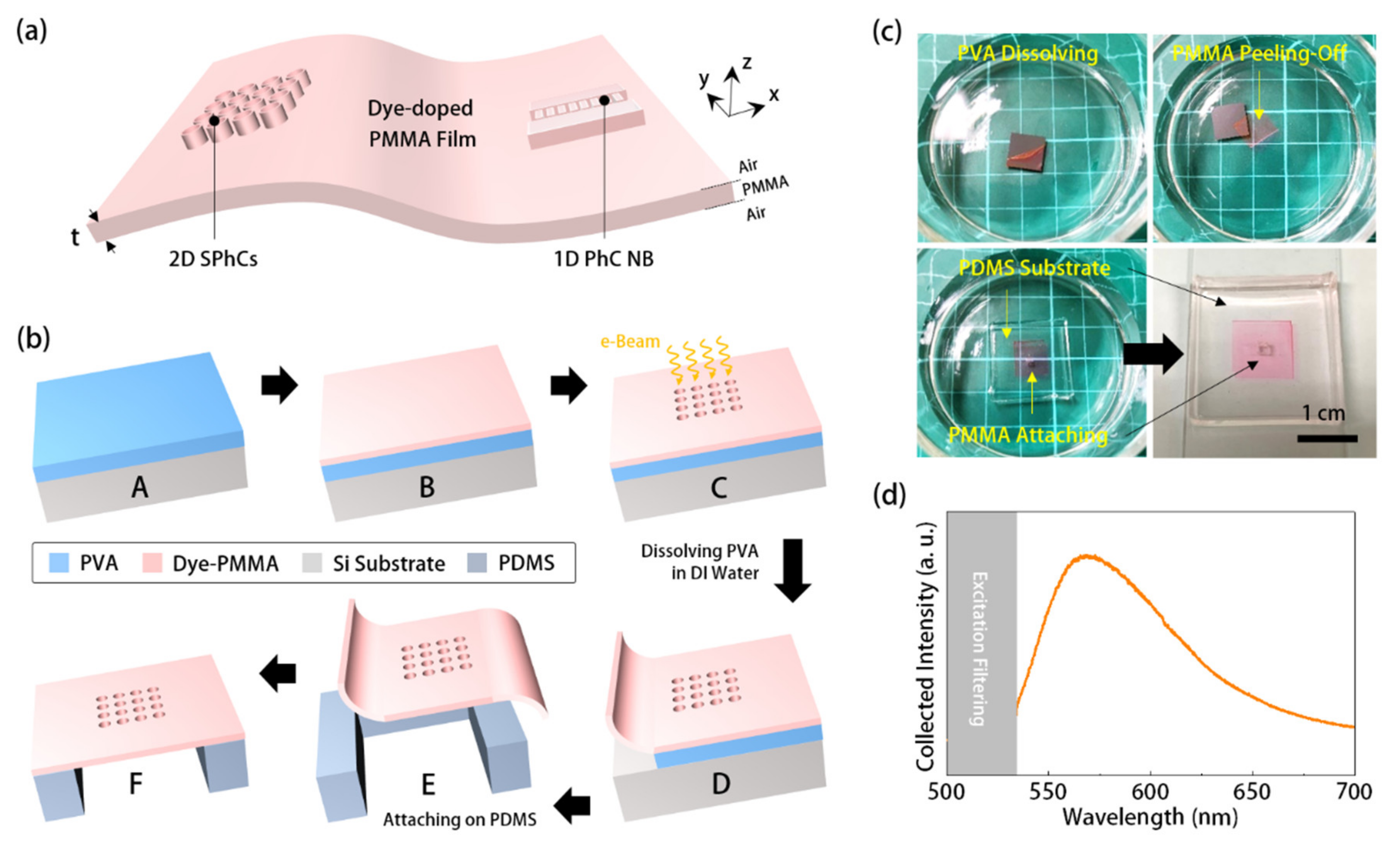
Figure 1a shows schematics of the thin-film PhC dye-laser we studied in this report. It includes two kinds of PhC resonators manufactured on a polymeric thin film (with a thickness of
t) suspended in the air. The thin film, with a refractive index
n of 1.49, is doped with chemical dyes as the gain medium. The PhC resonator design includes two-dimensional (2D) square PhCs (SPhCs) and one-dimensional (1D) PhC nanobeam (NB) cavity. In realizing the above structure, the manufacturing process in
Figure 1b started with (Step
A) spin-coating a polyvinyl-alcohol (PVA) interlayer (1000 rpm for 60 s, followed by 3000 rpm for 60 s) on a silicon substrate. We prepared the dye-doped polymer by dissolving the chemical dye PM-597 (Exciton Inc.) in poly-methylmethacrylate (PMMA, 950 K) with a concentration of 25 μmol/g. Afterward, we (Step
B) spin-coated the dye-doped PMMA onto the PVA layer (1000 rpm for 10 s, followed by 3500 rpm for 25 s), which produced a PMMA layer with a thickness of 300 nm. After soft baking at 90 °C for 180 s, we (Step
C) directly defined and manufactured the PhC patterns on the dye-doped PMMA layer by electron beam (
e-beam) lithography. Then, in Steps
D and
E, we immersed the sample in deionized (DI) water to dissolve the PVA interlayer and separate the patterned PMMA thin film from the silicon substrate. Finally, we (Step
F) attached the PMMA thin film onto a polydimethylsiloxane (PDMS) substrate with a via-hole to form a thin film structure suspending in the air. This step also means that one can attach this patterned PMMA thin film onto any other suitable surface or objects. The pictures in
Figure 1c show the process from Steps
D to
F. We then excited the dye-doped PMMA thin film using a 532 nm laser at room temperature to confirm its optical emission. The measured photoluminescence (PL) spectrum in
Figure 1d shows a broad emission spectral linewidth of about 80 nm centered at 570 nm. Therefore, the thickness of the PMMA thin film (
t = 300 nm) was between
λ/2
n and
λ/
n, where
λ represents the emission peak of dye-doped PMMA thin film. This thickness guaranteed that the PMMA thin film, as a planar waveguide in our proposed structure, only supports a transverse-electric-like (
TE-like) fundamental mode.
3. Mode Analysis and Lasing Actions from 1D and 2D PhC Resonators
For the first PhC resonator design, schematics in
Figure 2a define the lattice parameters of the 2D SPhCs, including lattice constant
a and radius
r. For the 2D SPhCs with an
a and
r/
a of 430 nm and 0.25 on the PMMA thin film with
t = 300 nm, we calculated its
TE-like band diagram using the three-dimensional (3D) plane-wave-expansion (PWE) method, as shown in
Figure 2b. In
Figure 2b, our interested mode candidate is the band-edge (BE) of the dielectric band (the first band, red dispersion curve) near the
Γ point, denoted as
Γ1 BE mode. Its frequency (
a/
λ ~ 0.75) aligns with the emission peak of PM-597 dye in
Figure 1d. In
Figure 2a,b, the theoretical
EX,
EY, and
Et fields of
Γ1 BE mode by 3D finite-element method (FEM, COMSOL Multiphysics software package) and PWE simulations all highly concentrate within the dielectric region. These field concentrations guarantee the strong light-matter interactions between the gain medium and
Γ1 BE mode. The flat band near the band-edge standing for low group velocity can also enhance the light-matter interaction in temporal. Furthermore, the BE mode near
Γ point also means the almost-zero in-plane wave vector can produce vertical radiations when serving as lasers.
Figure 2a shows the scanning electron microscope (SEM) image of the 2D SPhCs on a dye-doped PMMA, manufactured by the process in
Figure 1b, which is within an area of 50
a × 50
a. We excited it by using a 532 nm laser pulse with a pulse width of 0.5 ns, a repetition rate of 1 kHz, and a spot size of 8 μm in diameter, at room temperature.
Figure 2c and its inset show the measured spectra under excitation powers from 20.4 to 33.6 μW and the picture of light emission (the orange light spot) from the dye-doped PMMA film with 2D SPhCs under excitation.
Figure 2d further shows the collected power (light-in-light-out (
L-L) curve) and spectral linewidth variations of the optical emissions of the 2D SPhCs under different excitation powers. The curves’ bending clearly indicate the lasing action with a threshold of 29 μW. To prove this lasing action comes from the
Γ1 BE mode, instead of the dye itself, we further characterized the emissions from 2D SPhCs with different lattice parameters. In
Figure 2e, for the 2D SPhCs with a fixed
r/
a of 0.26 and increased
a from 430 to 475 nm, the lasing wavelengths showed significant red shifting. Furthermore, in
Figure 2f, with a fixed
a of 445 nm, the lasing wavelengths of 2D SPhCs showed a blue shifting when the
r/
a increased from 0.165 to 0.28. These wavelength shifts, caused by different lattice parameters, are the features of photonic modes in PhCs. It thus confirms the laser emissions come from the
Γ1 BE mode in 2D SPhCs.
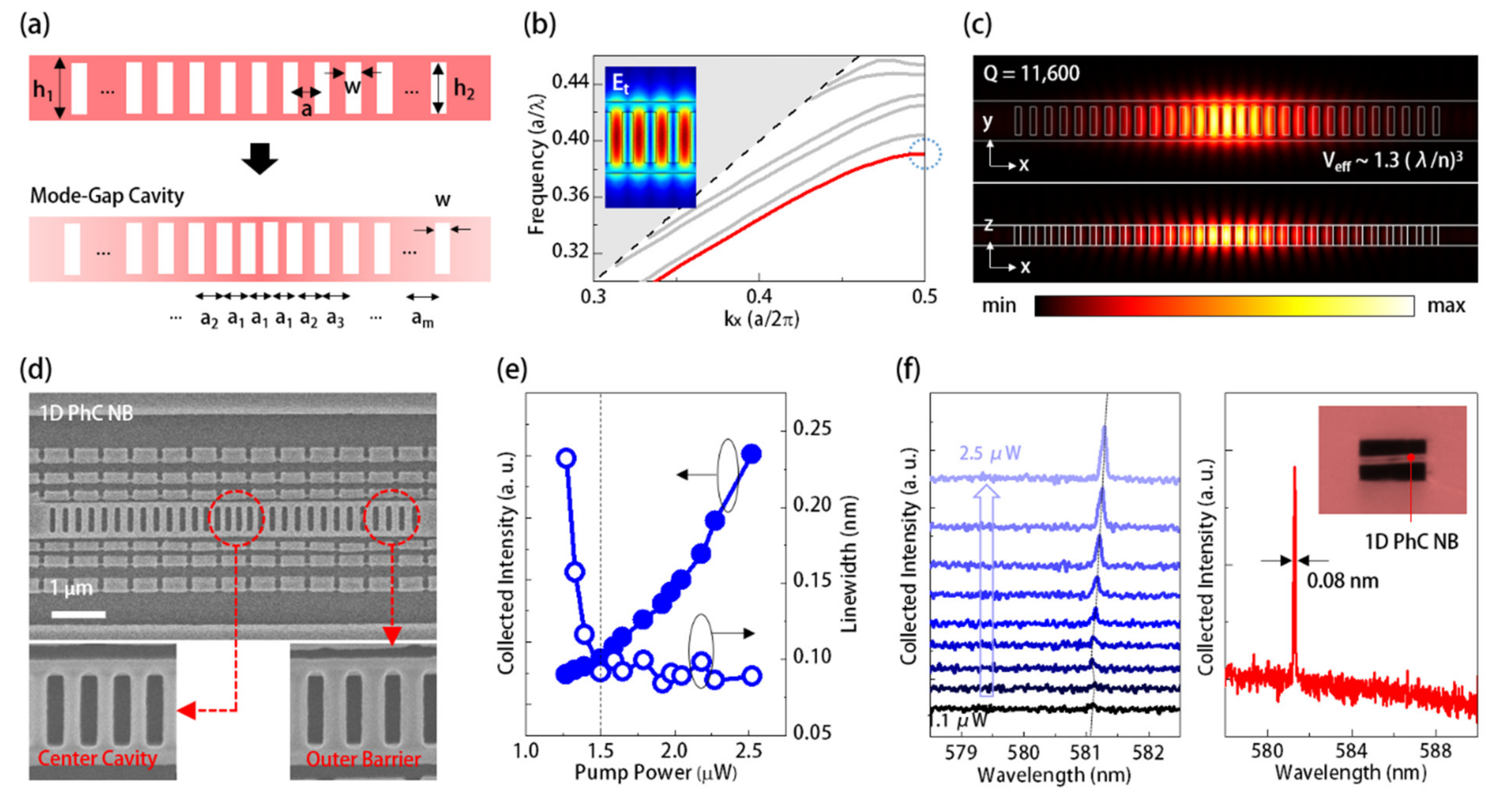
In the second kind of PhC resonator design, the 1D PhC NB consisted of periodic rectangular holes with height
h2 and width
w arranged along a suspended dye-doped PMMA waveguide with width
h1, as defined in
Figure 3a. In
Figure 3b, the theoretical
TE-like band diagram of the 1D PhC NB by the PWE method showed that the first band was a dielectric band, which is beneficial for realizing nanolasers. To effectively locally confine this dielectric band, we linearly increased the lattice constant of PhCs by 5 nm from the center to the edges of the NB to form a nanocavity, as illustrated in
Figure 3a. Although PMMA produces low index contrast (0.49) relative to the air when guiding the optical wave in the PhC NB, the above double hetero-lattice design provided a mode-gap effect [
17] for locally confining and tailoring the dielectric mode. Theoretical
Et field distributions of the confined dielectric mode along
XY- and
XZ-planes in
Figure 3c clearly show its field concentration within the nanocavity region. In the case of the 15 holes on each side of the nanocavity (i.e., the
m defined in
Figure 3a is 14), the confined dielectric mode is with a sufficiently high-quality factor (
Q) of 11,600 and a small effective mode volume (
Veff) of 1.26 (
λ/
n)
3. This high
Q/
Veff value is beneficial for providing strong light-matter interactions as a mode candidate in a nanolaser.
Figure 3d shows the top and zoom-in view SEM pictures of the manufactured 1D PhC NB cavity on a dye-doped PMMA thin film before separating from the silicon substrate. By the same excitation condition for 2D SPhCs,
Figure 3e shows the
L-L curve and spectral linewidths under different excitation powers from 1.5 to 2.5 μW, where the curves’ bending indicate a low lasing threshold of 1.5 μW.
Figure 3f shows the corresponding lasing spectra, which show a narrow spectral lasing linewidth of 0.08 nm. It should be noted that the threshold of the dye-laser based on the 1D PhC NB cavity is one order lower than that of the
Γ1 BE mode in the 2D SPhCs in
Figure 2d. This low threshold comes from the strong light-matter interactions provided by the confined dielectric mode with a high
Q/
Veff value and the reduced redundant gain medium by a small device footprint of the 1D PhC NB cavity. Although the
Γ1 BE mode in the 2D SPhCs has a much higher threshold, its strong emissions, standing for a high signal-to-noise (
S/N) ratio, is still beneficial for optical sensing.
In addition, owing to the high excitation laser pulse repetition rate (1 kHz), all the activated PhC dye-lasers will be at least exposed to over 5 × 10
5 excitation pulses during a power-dependence PL measurement. However, we did not observe significant intensity degradation or wavelength blue shift caused by the bleaching of the dye, as shown in
Figure 2c,d and
Figure 3e,f. Therefore, we believe the dye-lasers presented could handle tens of minutes to several hours of accumulated operation time, under a lower excitation repetition rate of several tens Hz, which is long enough for executing sensing applications.
4. Evaluating on Feasibility as an Attachable Strain Sensor
In addition to a low-cost visible laser, the single-mode lasing action and narrow spectral linewidth are also beneficial for providing a sufficient
S/N ratio and spectral resolution in optical sensing applications. Owing to the elastic thin film structure, the PhC dye-lasers presented herein could further be used as a strain sensor, capable of on-demand attachment to analyzed object surfaces. To confirm the feasibility of this idea, we first investigated the lasing properties of the PhC dye-lasers after attaching them to an object’s surface. In the manufacturing process, we separated the dye-doped PMMA thin film from the silicon substrate and attached it to filter paper in DI water. The picture and OM image in
Figure 4a show the dye-doped PMMA thin film with the 2D SPhCs with different lattice constants on filter paper. In measurements, the attached 2D SPhC dye-lasers retain almost the same lasing wavelength in the case of suspending it in the air, as shown in
Figure 4b. These invariant wavelengths come from attaching to a surface with roughness much larger than the wavelength scale, which makes the 2D SPhCs equivalent to suspension in the air, as illustrated by the inset of
Figure 4b. The lasing wavelength also showed the same trend of increasing with the lattice constant. Therefore, we confirmed our presented PhC dye-lasers were still workable when attached to the analyzed object surface, particularly to a surface with a roughness larger than
λ. In addition, it of note that this thin film with PhC dye-lasers can be transferred to the other object’s surface by merely repeating the above-attaching process in water, which means it has reusability when serving as an attachable strain sensor.
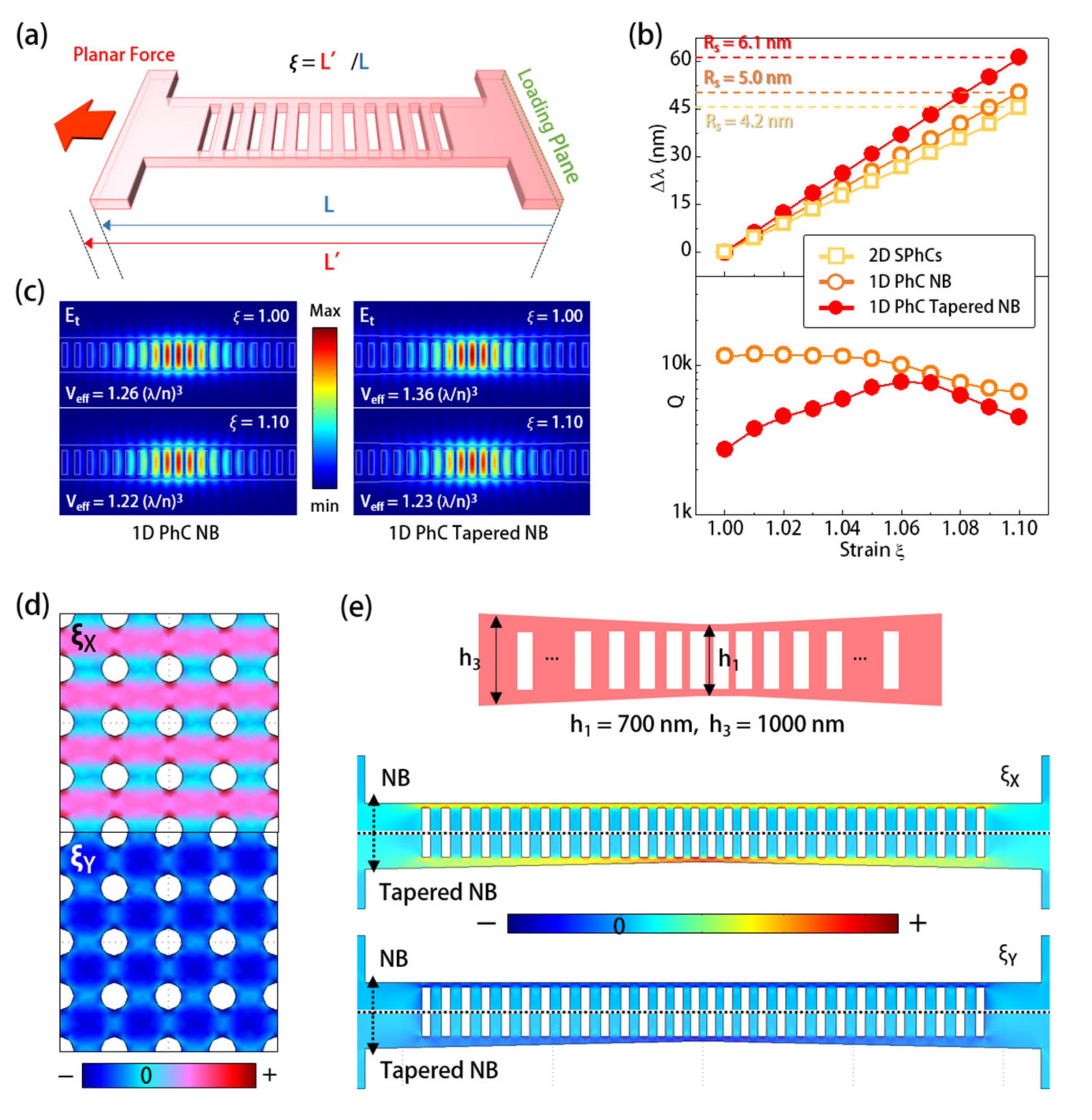
To theoretically investigate the capabilities of strain sensing of the 2D SPhCs and 1D PhC NB cavity, we applied a stretching strain
ξ to them along the
X-direction and characterized their optical responses by the FEM simulation setup in
Figure 5a. In
Figure 5a, we set a loading plane on one side of the PMMA thin film with PhC resonators and applied a planar force on the opposite side. The applied stretching strain ξ was defined as the length ratio of the sample before (
L) and after (
L′) applying stretching.
Figure 5b shows the wavelength shifts of these two resonator designs under every 1%
ξ variation (defined as strain response
RS) under the applied
ξ from 1.00 to 1.10, which correspond to an
RS of 4.2 and 5.0 nm, respectively. In evaluating the strain sensing capability, the expression
Δλ/
RS defined the minimum detectable strain variation
Δξdet, where
Δλ represents the spectral linewidth of the utilized mode decided by
λ/Q in a passive PhC resonator. However, in an active resonator,
Δλ represents the lasing spectral linewidth, which is 0.08 nm as shown in
Figure 2c and
Figure 3e, while the
Q value mainly determines the lasing threshold level. Therefore, the
RS values of the utilized modes, depending on PhC lattice structures and device topologies, will determine the sensing performance. In addition to sensing performance, the utilized mode stability in PhC dye-lasers under the applied strain is also important for the strain sensor. For example,
Figure 5b shows theoretical
Q values of dielectric mode in the 1D PhC NB cavity under
ξ from 1.00 to 1.10, where
Q is almost invariant under
ξ < 1.05 and only slightly degraded with an enlarged
ξ under
ξ > 1.05. In
Figure 5c, the theoretical
Et fields and
Veff of the dielectric mode in the 1D PhC NB cavity under
ξ of 1.00 and 1.10 were also almost invariant. These properties mean the dielectric mode can be well maintained inside the nanocavity under the applied
ξ, which thus guarantees stable laser properties during strain sensing.
Figure 5d,e shows the theoretical strain distributions, along the
X- (ξ
X) and
Y-directions (
ξY) of the above PhC resonator designs, under the applied stretching strain
ξ along the X-direction, which can explain their difference in
RS value. In the case of 2D SPhCs, although the resulted
ξX stretched the lattice along the
X-direction, the resultant
ξY compressed the lattice instead along the
Y-direction because of the positive Poisson ratio (~0.33) of PMMA, as shown in
Figure 5d. That means the responses of
Γ1 BE mode to the applied strain will be different in different lattice directions, which thus limits its
RS value. On the contrary, in the case of the 1D PhC NB, because the lattices are arranged along only one direction, the
ξX in
Figure 5e thus becomes the only shaper to the lattices and dielectric mode inside, while
ξY only slightly compresses the NB along the
Y-direction without significantly deforming the lattices. Therefore, the dielectric mode in the 1D PhC NB cavity had a higher
RS of 5.0 nm.
To further enhance the
RS of the dielectric mode in the 1D PhC NB, we modified the NB to have a tapered width by
h1 to
h3, as shown in
Figure 5e. This non-uniform NB design, based on the concept of strain shaping [
18,
19,
20], can concentrate more strain in the narrow region (center of NB) under uniformly applied stress. In
Figure 5e, the comparison between theoretical
ξX of the 1D PhC tapered and untapered NB cavities clearly confirmed this kind of strain concentration. Even the
ξY for slightly compressing the NB was also minimized in this tapered NB design, as shown in
Figure 5e. Therefore, via the maximized
ξX, this design can produce an improved
RS value of 6.1 nm, as shown in
Figure 5b. In addition, in
Figure 5b,c, the theoretical
Q and
Veff of the dielectric mode in this tapered NB cavity also showed small variations under different applied
ξ, which can guarantee stable laser properties during strain sensing. As a strain sensor, according to the expression
Δλ/
RS, with a lasing spectral linewidth
Δλ of 0.08 nm in
Figure 3f and an
RS of 6.1 nm, the theoretical
Δξdet of the dielectric mode in the 1D PhC tapered NB cavity could be 1.3 × 10
−4, which is smaller than that (~2.0 × 10
−4) provided by the
Γ1 BE mode in the 2D SPhCs. Moreover, according to the
ξX and
ξY distributions in
Figure 5e, it is reasonable to assume that we could further enhance the
Rs value of the dielectric mode in the tapered NB cavity by enlarging the ratio between the NB side walls widths near and away from the cavity region, i.e., enlarging the value of (
h3-
h2)/(
h1-
h2), to concentrate more strain near the cavity region. However, it would also accompany
Q degradation, as shown in
Figure 5b.
On the other hand, because of the high thermo-optic coefficient of PMMA used herein, our proposed PhC dye-lasers would also be suitable for temperature sensing. In evaluating the sensing response, the wavelength shifts
λT (in a unit of nm/K) of the dielectric mode in the 1D PhC NB cavity, caused by temperature variation, can be expressed as:
where α is the coefficient of thermal expansion in a unit of K
−1, which represents the material expansion with temperature.
Rv represents the dielectric mode wavelength shift 1% isotropic expansion of the PhC NB. We should note that this
Rv is different from the
Rs obtained from the NB under an anisotropic expansion by the positive Poisson ratio. The α ×
Rv term thus represents the dielectric mode wavelength shift caused by the PhC NB expansion with temperature. In the (
dn/
dT) ×
Ri term, the thermo-optic coefficient
dn/
dT represents the PhC NB refractive index change with temperature, while
Ri represents the dielectric mode wavelength shift caused by the PhC NB refractive index change. Therefore, the (
dn/
dT) ×
Ri term represents the dielectric mode wavelength shift caused by the PhC NB refractive index change with temperature. For the PMMA (950 K) used in this report, α and
dn/
dT were approximately 4.2 × 10
−5 K
−1 and −3.2 × 10
−4 K
−1, respectively. The theoretical
Rv and
Ri of the dielectric mode in the 1D PhC tapered NB cavity were 5.8 and 289 nm, respectively. According to Equation (1), the theoretical
λT of the dielectric mode can be determined as −0.068 nm/K. Considering the minimum linewidth (0.08 nm) of the NB laser presented herein, its minimum detectable temperature variation
ΔTdet would be 1.2 K when serving as a temperature sensor. For the
Γ1 BE mode with
Rv and
Ri of 5.9 and 220 nm, its theoretical
λT of −0.046 nm/K would result in a
ΔTdet of 1.7 K.


