Scalable and High-Throughput Top-Down Manufacturing of Optical Metasurfaces

 , , and
Abstract
1. Introduction
2. Optical Methods
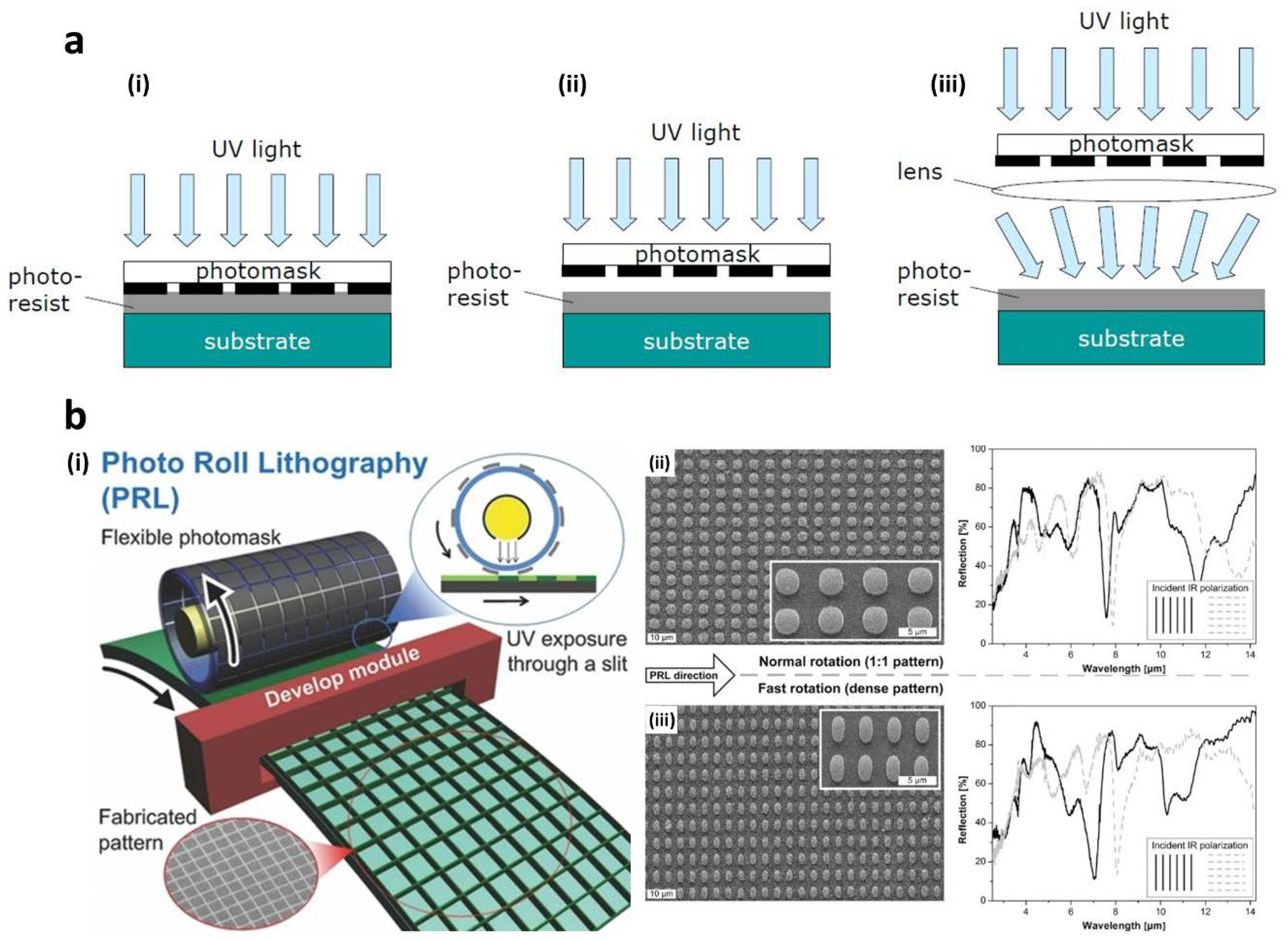
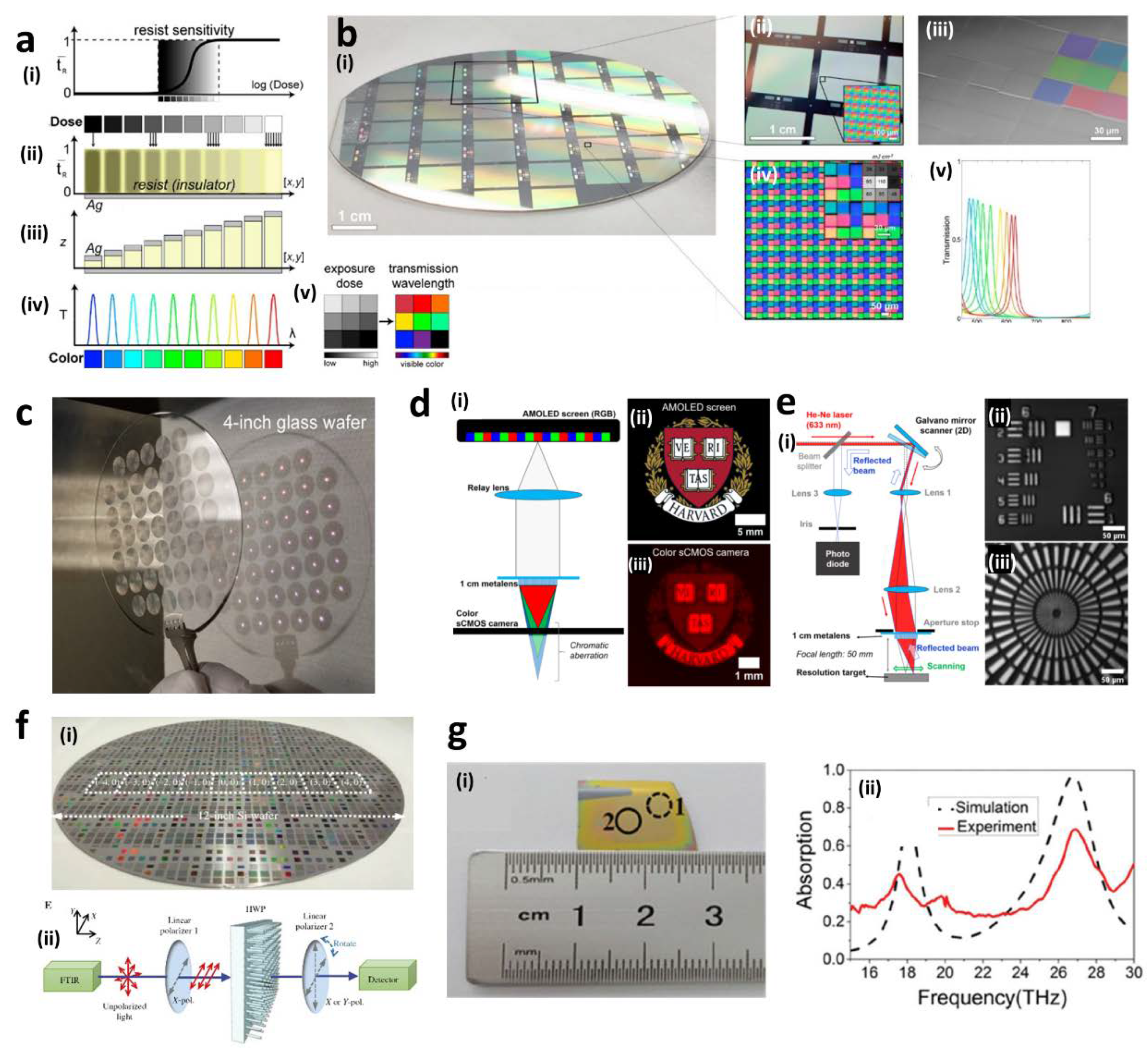
2.1. Conventional Photolithography
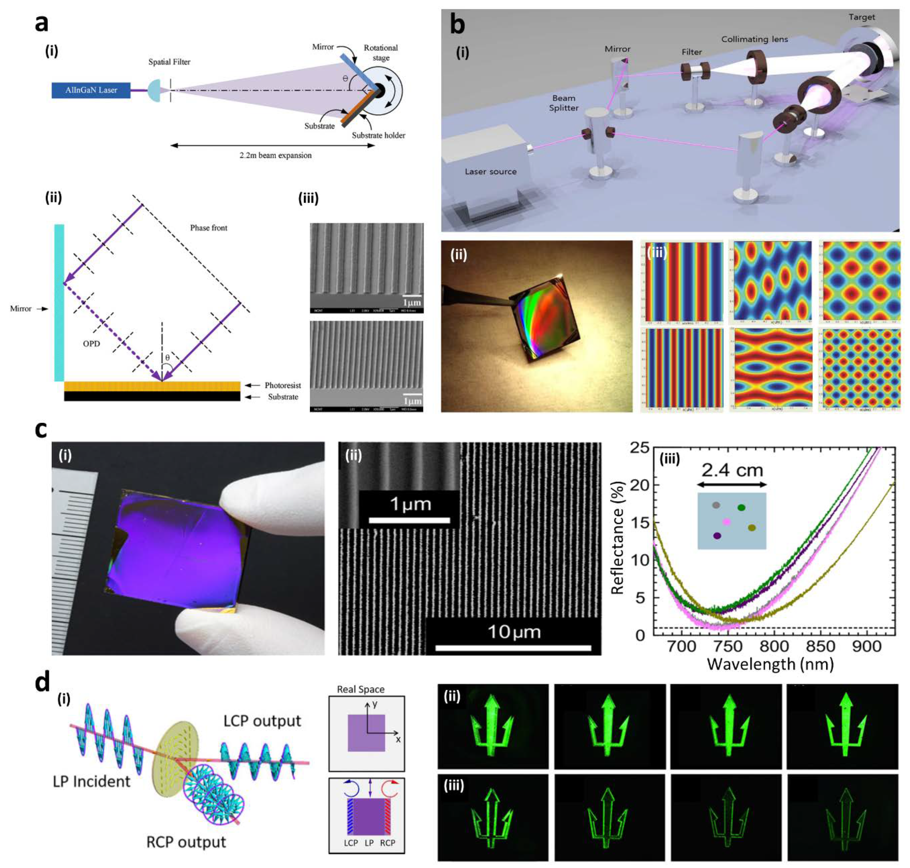
2.2. Interference Lithography (IL)
2.2.1. Optics-Based IL
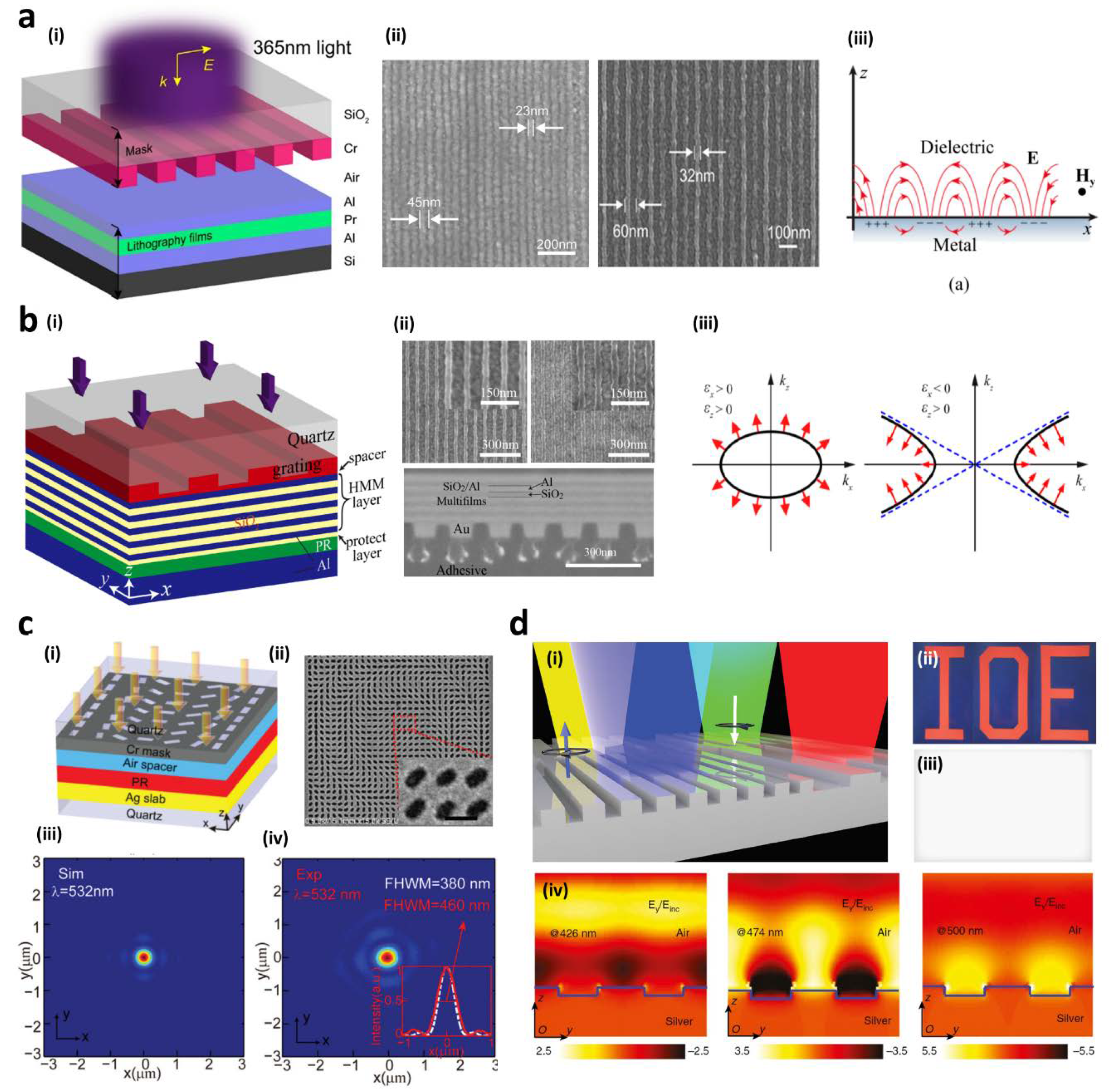
2.2.2. Plasmonic-Based Interference Lithography
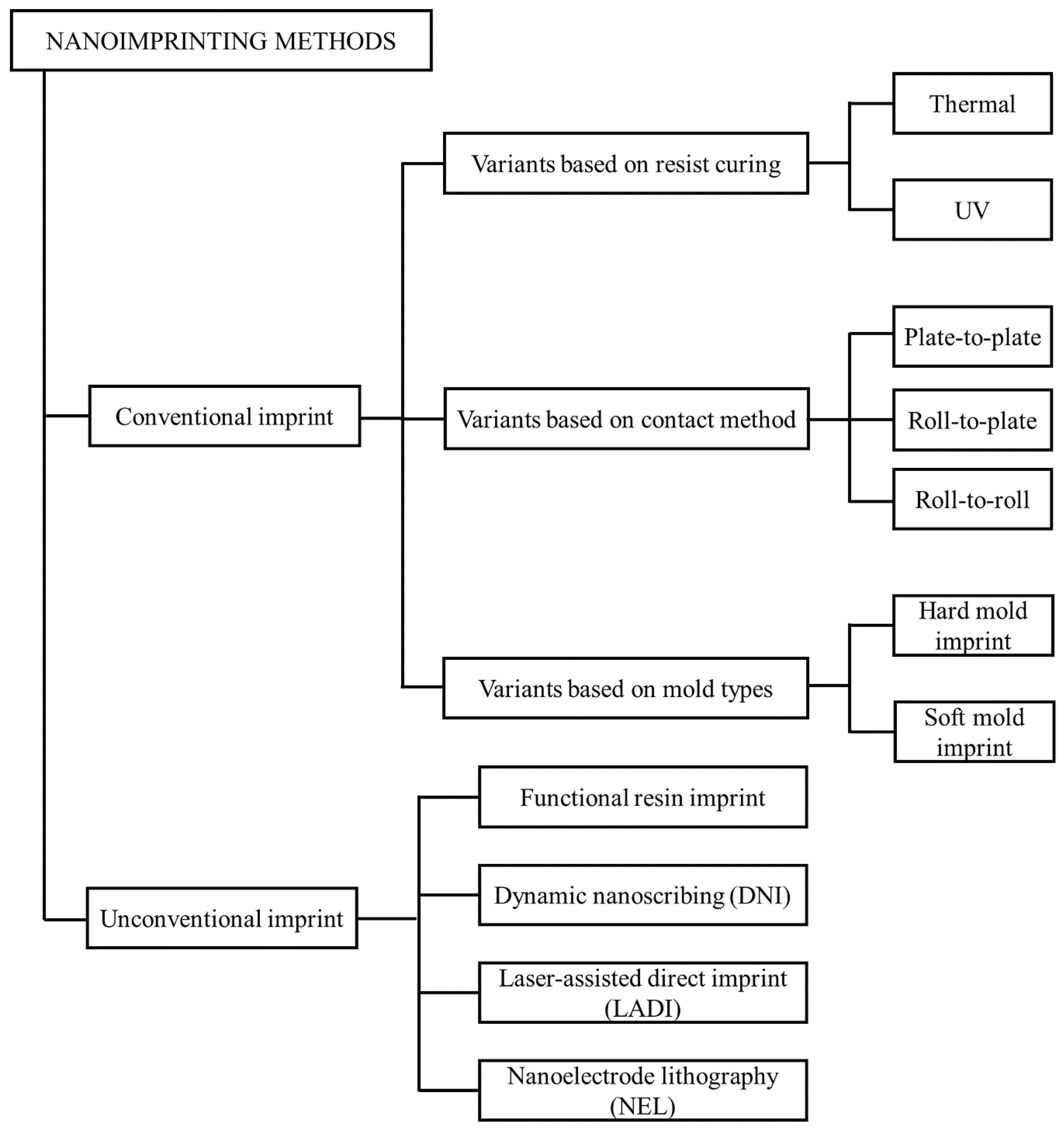
3. Printing Methods
3.1. Conventional Printing Methods
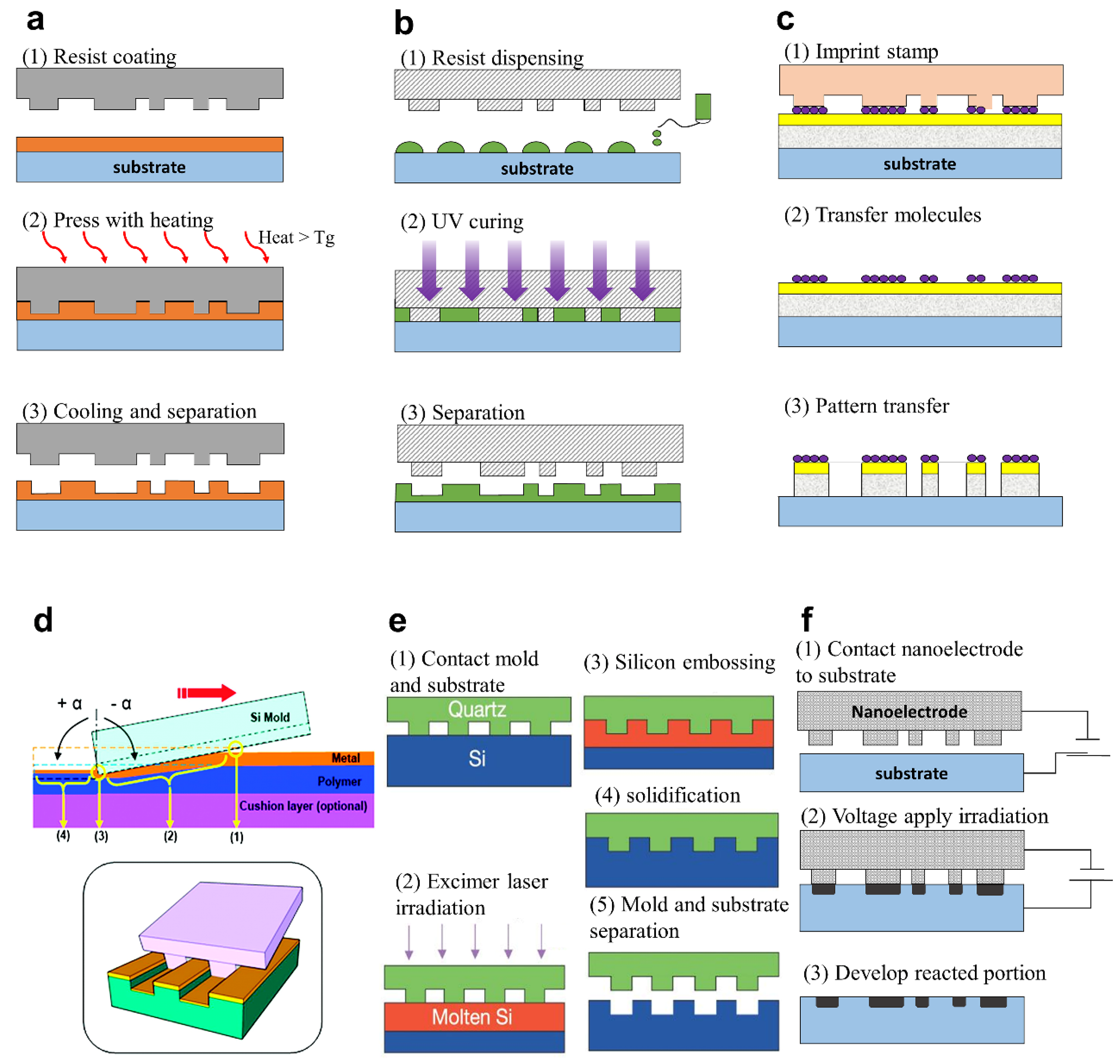
3.1.1. Curing Source
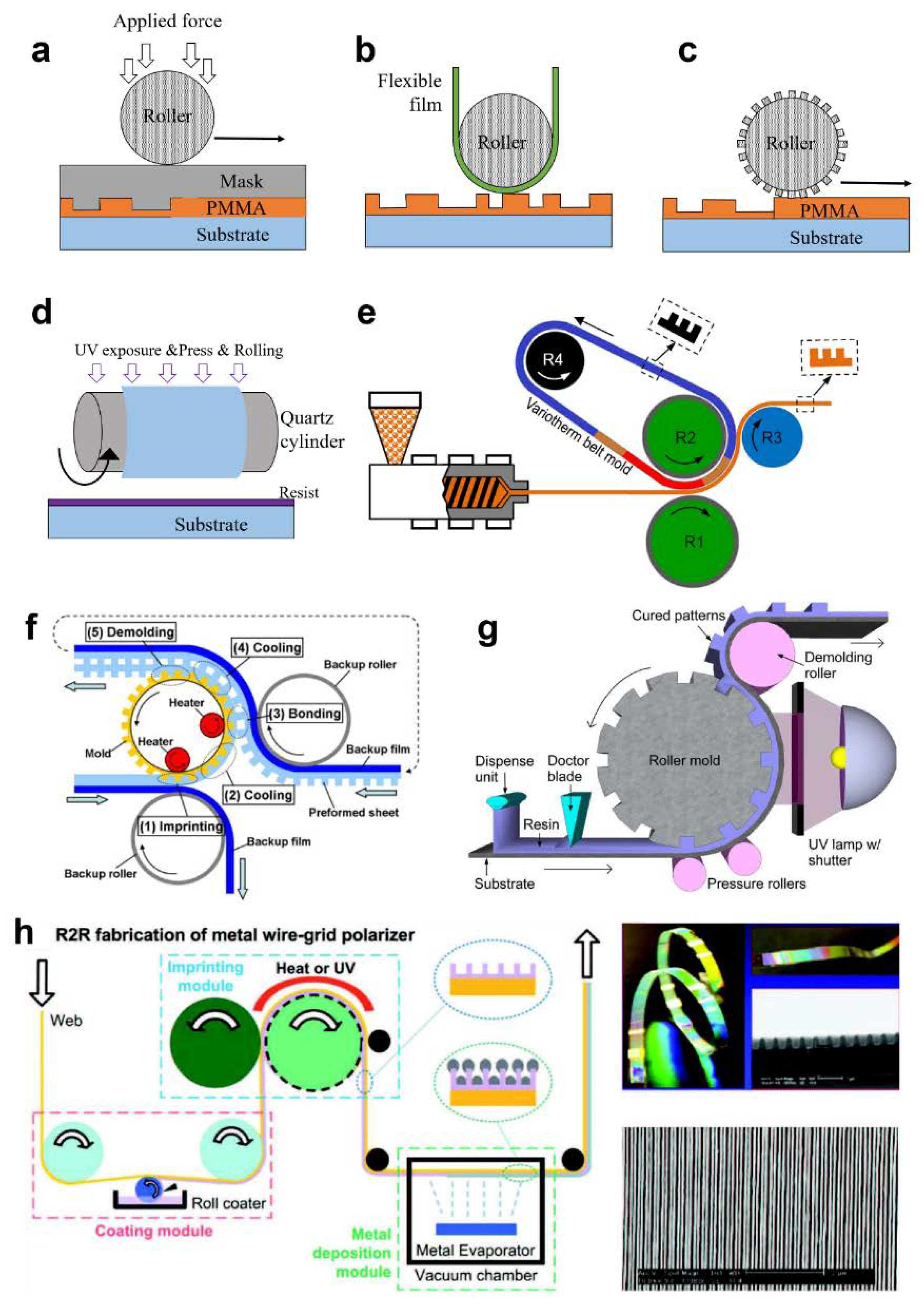
3.1.2. Contact Type
3.1.3. Mold Type
3.2. Unconventional Printing Methods
4. Conclusions and Outlook
Author Contributions
Funding
Acknowledgments
Conflicts of Interest
References
- Park, S.; Lee, G.; Park, B.; Seo, Y.; bin Park, C.; Chun, Y.T.; Joo, C.; Rho, J.; Kim, J.M.; Hone, J.; et al. Electrically focus-tuneable ultrathin lens for high-resolution square subpixels. Light Sci. Appl. 2020, 9, 98. [Google Scholar] [CrossRef] [PubMed]
- Yoon, G.; Kim, K.; Huh, D.; Lee, H.; Rho, J. Single-step manufacturing of hierarchical dielectric metalens in the visible. Nat. Commun. 2020, 11, 2268. [Google Scholar] [CrossRef] [PubMed]
- Wong, Z.J.; Wang, Y.; O’Brien, K.; Rho, J.; Yin, X.; Zhang, S.; Fang, N.; Yen, T.-J.; Zhang, X. Optical and acoustic metamaterials: Superlens, negative refractive index and invisibility cloak. J. Opt. 2017, 19, 84007. [Google Scholar] [CrossRef]
- Lee, D.; Kim, Y.D.; Kim, M.; So, S.; Choi, H.-J.J.; Mun, J.; Nguyen, D.M.; Badloe, T.; Ok, J.G.; Kim, K.; et al. Realization of Wafer-Scale Hyperlens Device for Sub-diffractional Biomolecular Imaging. ACS Photonics 2018, 5, 2549–2554. [Google Scholar] [CrossRef]
- Byun, M.M.; Lee, D.; Kim, M.; Kim, Y.; Kim, K.; Ok, J.G.; Rho, J.; Lee, H. Demonstration of nanoimprinted hyperlens array for high-throughput sub-diffraction imaging. Sci. Rep. 2017, 7, 1–11. [Google Scholar] [CrossRef] [PubMed]
- Kim, M.; Kim, I.; Jang, J.; Lee, D.; Nam, K.; Rho, J. Active Color Control in a Metasurface by Polarization Rotation. Appl. Sci. 2018, 8, 982. [Google Scholar] [CrossRef]
- Kim, I.; Yoon, G.; Jang, J.; Genevet, P.; Nam, K.T.; Rho, J. Outfitting Next Generation Displays with Optical Metasurfaces. ACS Photonics 2018, 5, 3876–3895. [Google Scholar] [CrossRef]
- Jang, J.; Kang, K.; Raeis-Hosseini, N.; Ismukhanova, A.; Jeong, H.; Jung, C.; Kim, B.; Lee, J.-Y.; Park, I.; Rho, J. Self-Powered Humidity Sensor Using Chitosan-Based Plasmonic Metal–Hydrogel–Metal Filters. Adv. Opt. Mater. 2020, 8, 1901932. [Google Scholar] [CrossRef]
- Jang, J.; Jeong, H.; Hu, G.; Qiu, C.-W.; Nam, K.T.; Rho, J. Kerker-Conditioned Dynamic Cryptographic Nanoprints. Adv. Opt. Mater. 2019, 7, 1801070. [Google Scholar] [CrossRef]
- Yoon, G.; Lee, D.; Nam, K.T.; Rho, J. “Crypto-Display” in Dual-Mode Metasurfaces by Simultaneous Control of Phase and Spectral Responses. ACS Nano 2018, 12, 6421–6428. [Google Scholar] [CrossRef]
- Lee, T.; Jang, J.; Jeong, H.; Rho, J. Plasmonic- and dielectric-based structural coloring: From fundamentals to practical applications. Nano Converg. 2018, 5. [Google Scholar] [CrossRef] [PubMed]
- Fleischman, D.; Sweatlock, L.A.; Murakami, H.; Atwater, H. Hyper-selective plasmonic color filters. Opt. Express 2017, 25, 27386–27395. [Google Scholar] [CrossRef] [PubMed]
- Aoni, R.A.; Rahmani, M.; Xu, L.; Zangeneh Kamali, K.; Komar, A.; Yan, J.; Neshev, D.; Miroshnichenko, A.E. High-Efficiency Visible Light Manipulation Using Dielectric Metasurfaces. Sci. Rep. 2019, 9, 6510. [Google Scholar] [CrossRef]
- Ansari, M.A.; Kim, I.; Rukhlenko, I.D.; Zubair, M.; Yerci, S.; Tauqeer, T.; Mehmood, M.Q.; Rho, J. Engineering spin and antiferromagnetic resonances to realize an efficient direction-multiplexed visible meta-hologram. Nanoscale Horiz. 2020, 5, 373. [Google Scholar] [CrossRef]
- Yoon, G.; Kim, J.; Mun, J.; Lee, D.; Nam, K.T.; Rho, J. Wavelength-decoupled geometric metasurfaces by arbitrary dispersion control. Commun. Phys. 2019, 2, 129. [Google Scholar] [CrossRef]
- Kim, K.; Yoon, G.; Baek, S.; Rho, J.; Lee, H. Facile Nanocasting of Dielectric Metasurfaces with Sub-100 nm Resolution. ACS Appl. Mater. Interfaces 2019, 11, 26109–26115. [Google Scholar] [CrossRef] [PubMed]
- Ansari, M.A.; Kim, I.; Lee, D.; Waseem, M.H.; Zubair, M.; Mahmood, N.; Badloe, T.; Yerci, S.; Tauqeer, T.; Mehmood, M.Q.; et al. A Spin-Encoded All-Dielectric Metahologram for Visible Light. Laser Photon. Rev. 2019, 13, 1900065. [Google Scholar] [CrossRef]
- Yoon, G.; Lee, D.; Nam, K.T.; Rho, J. Pragmatic Metasurface Hologram at Visible Wavelength: The Balance between Diffraction Efficiency and Fabrication Compatibility. ACS Photonics 2017, 5, 1643–1647. [Google Scholar] [CrossRef]
- Lee, G.-Y.; Yoon, G.; Lee, S.-Y.; Yun, H.; Cho, J.; Lee, K.; Kim, H.; Rho, J.; Lee, B. Complete amplitude and phase control of light using broadband holographic metasurfaces. Nanoscale 2018, 10, 4237–4245. [Google Scholar] [CrossRef]
- Li, Z.; Kim, I.; Zhang, L.; Mehmood, M.Q.; Anwar, M.S.; Saleem, M.; Lee, D.; Nam, K.T.; Zhang, S.; Luk’yanchuk, B.; et al. Dielectric Meta-Holograms Enabled with Dual Magnetic Resonances in Visible Light. ACS Nano 2017, 11, 9382–9389. [Google Scholar] [CrossRef]
- Lee, D.; Yang, Y.; Yoon, G.; Kim, M.; Rho, J. Resolution enhancement of fluorescence microscopy using encoded patterns from all-dielectric metasurfaces. Appl. Phys. Lett. 2019, 115, 101102. [Google Scholar] [CrossRef]
- Kim, M.; Rho, J. Metamaterials and imaging. Nano Converg. 2015, 2, 22. [Google Scholar] [CrossRef] [PubMed]
- Lee, D.; Kim, M.; Kim, J.; Hong, H.; Badloe, T.; Sung Kim, D.; Rho, J. All-dielectric metasurface imaging platform applicable to laser scanning microscopy with enhanced axial resolution and wavelength selection. Opt. Mater. Express 2019, 9, 3248–3259. [Google Scholar] [CrossRef]
- Kim, I.; So, S.; Rana, A.S.; Mehmood, M.Q.; Rho, J. Thermally robust ring-shaped chromium perfect absorber of visible light. Nanophotonics 2018, 7, 1827–1833. [Google Scholar] [CrossRef]
- Lee, D.; Han, S.Y.; Jeong, Y.; Nguyen, D.M.; Yoon, G.; Mun, J.; Chae, J.; Lee, J.H.; Ok, J.G.; Jung, G.Y.; et al. Polarization-sensitive tunable absorber in visible and near-infrared regimes. Sci. Rep. 2018, 8, 12393. [Google Scholar] [CrossRef] [PubMed]
- Rana, A.S.; Mehmood, M.Q.; Jeong, H.; Kim, I.; Rho, J. Tungsten-based Ultrathin Absorber for Visible Regime. Sci. Rep. 2018, 8, 2443. [Google Scholar] [CrossRef] [PubMed]
- Yoon, G.; So, S.; Kim, M.; Mun, J.; Ma, R.; Rho, J. Electrically tunable metasurface perfect absorber for infrared frequencies. Nano Converg. 2017, 4, 36. [Google Scholar] [CrossRef]
- Badloe, T.; Mun, J.; Rho, J. Metasurfaces-Based Absorption and Reflection Control: Perfect Absorbers and Reflectors. J. Nanomater. 2017, 2017, 1–18. [Google Scholar] [CrossRef]
- Nguyen, D.M.; Lee, D.; Rho, J. Control of light absorbance using plasmonic grating based perfect absorber at visible and near-infrared wavelengths. Sci. Rep. 2017, 7, 2611. [Google Scholar] [CrossRef]
- Rajasekharan, R.; Butt, H.; Dai, Q.; Wilkinson, T.D.; Amaratunga, G.A.J. Can Nanotubes Make a Lens Array? Adv. Mater. 2012, 24, 170–173. [Google Scholar] [CrossRef]
- Yoon, G.; Lee, D.; Rho, J. Demonstration of Equal-Intensity Beam Generation by Dielectric Metasurfaces. J. Vis. Exp. 2019, 148, 59066. [Google Scholar] [CrossRef] [PubMed]
- Li, Z.; Dai, Q.; Mehmood, M.Q.; Hu, G.; Yanchuk, B.L.; Tao, J.; Hao, C.; Kim, I.; Jeong, H.; Zheng, G.; et al. Full-space Cloud of Random Points with a Scrambling Metasurface. Light Sci. Appl. 2018, 7, 63. [Google Scholar] [CrossRef] [PubMed]
- Yoon, G.; Lee, D.; Nam, K.T.; Rho, J. Geometric metasurface enabling polarization independent beam splitting. Sci. Rep. 2018, 8, 9468. [Google Scholar] [CrossRef] [PubMed]
- Kim, M.; Lee, D.; Kim, T.H.; Yang, Y.; Park, H.J.; Rho, J. Observation of Enhanced Optical Spin Hall Effect in a Vertical Hyperbolic Metamaterial. ACS Photonics 2019, 6, 2530–2536. [Google Scholar] [CrossRef]
- Wang, Y.-H.; Jin, R.-C.; Li, J.-Q.; Zhong, F.; Liu, H.; Kim, I.; Jo, Y.; Rho, J.; Dong, Z.-G. Photonic spin Hall effect by the spin-orbit interaction in a metasurface with elliptical nano-structures. Appl. Phys. Lett. 2017, 110, 101908. [Google Scholar] [CrossRef]
- Yin, X.; Ye, Z.; Rho, J.; Wang, Y.; Zhang, X. Photonic Spin Hall Effect at Metasurfaces. Science (80-) 2013, 339, 1405–1407. [Google Scholar] [CrossRef]
- Wang, Y.-H.; Kim, I.; Jin, R.-C.; Jeong, H.; Li, J.-Q.; Dong, Z.-G.; Rho, J. Experimental verification of asymmetric transmission in continuous omega-shaped metamaterials. RSC Adv. 2018, 8, 38556–38561. [Google Scholar] [CrossRef]
- Mahmood, N.; Kim, I.; Mehmood, M.Q.; Jeong, H.; Akbar, A.; Lee, D.; Saleem, M.; Zubair, M.; Anwar, M.S.; Tahir, F.A.; et al. Polarisation insensitive multifunctional metasurfaces based on all-dielectric nanowaveguides. Nanoscale 2018, 10, 18323–18330. [Google Scholar] [CrossRef]
- Yoon, G.; Jang, J.; Mun, J.; Nam, K.T.; Rho, J. Metasurface zone plate for light manipulation in vectorial regime. Commun. Phys. 2019, 2, 156. [Google Scholar] [CrossRef]
- Mahmood, N.; Jeong, H.; Kim, I.; Mehmood, M.Q.; Zubair, M.; Akbar, A.; Saleem, M.; Anwar, M.S.; Tahir, F.A.; Rho, J. Twisted non-diffracting beams through all dielectric meta-axicons. Nanoscale 2019, 11, 20571–20578. [Google Scholar] [CrossRef]
- Lee, H.-E.; Ahn, H.-Y.; Mun, J.; Lee, Y.Y.; Kim, M.; Cho, N.H.; Chang, K.; Kim, W.S.; Rho, J.; Nam, K.T. Amino-acid- and peptide-directed synthesis of chiral plasmonic gold nanoparticles. Nature 2018, 556, 360–365. [Google Scholar] [CrossRef] [PubMed]
- Hong, J.; Kim, S.-J.; Kim, I.; Yun, H.; Mun, S.-E.; Rho, J.; Lee, B. Plasmonic metasurface cavity for simultaneous enhancement of optical electric and magnetic fields in deep subwavelength volume. Opt. Express 2018, 26, 13340–13348. [Google Scholar] [CrossRef] [PubMed]
- Raeis-Hosseini, N.; Rho, J. Metasurfaces Based on Phase-Change Material as a Reconfigurable Platform for Multifunctional Devices. Materials (Basel) 2017, 10, 1046. [Google Scholar] [CrossRef] [PubMed]
- Yoon, G.; Kim, I.; So, S.; Mun, J.; Kim, M.; Rho, J. Fabrication of three-dimensional suspended, interlayered and hierarchical nanostructures by accuracy-improved electron beam lithography overlay. Sci. Rep. 2017, 7, 6668. [Google Scholar] [CrossRef]
- Kim, I.; So, S.; Mun, J.; Lee, K.H.; Lee, J.H.; Lee, T.; Rho, J. Optical characterizations and thermal analyses of HfO 2/SiO 2 multilayered diffraction gratings for high-power continuous wave laser. J. Phys. Photonics 2020, 2, 025004. [Google Scholar] [CrossRef]
- Kim, M.; Mun, J.; Bae, D.; Jeon, G.; Go, M.C.; Rho, J.; Kim, J.K. Accordion-like plasmonic silver nanorod array exhibiting multiple electromagnetic responses. NPG Asia Mater. 2018, 10, 190–196. [Google Scholar] [CrossRef]
- Lanzillotti-Kimura, N.D.; O’brien, K.P.; Rho, J.; Suchowski, H.; Yin, X.; Zhang, X. Polarization-controlled coherent phonon generation in acoustoplasmonic metasurfaces. Phys. Rev. B 2018, 97, 1–5. [Google Scholar] [CrossRef]
- Yoon, G.; Kim, I.; Rho, J. Challenges in fabrication towards realization of practical metamaterials. Microelectron. Eng. 2016, 163, 7–20. [Google Scholar] [CrossRef]
- Lee, H.-E.; Kim, R.M.; Ahn, H.-Y.; Lee, Y.Y.; Byun, G.H.; Im, S.W.; Mun, J.; Rho, J.; Nam, K.T. Cysteine-encoded chirality evolution in plasmonic rhombic dodecahedral gold nanoparticles. Nat. Commun. 2020, 11, 263. [Google Scholar] [CrossRef]
- Sun, K.; Riedel, C.A.; Urbani, A.; Simeoni, M.; Mengali, S.; Zalkovskij, M.; Bilenberg, B.; de Groot, C.H.; Muskens, O.L. VO2 Thermochromic Metamaterial-Based Smart Optical Solar Reflector. ACS Photonics 2018, 5, 2280–2286. [Google Scholar] [CrossRef]
- Badloe, T.; Kim, I.; Rho, J. Moth-eye shaped on-demand broadband and switchable perfect absorbers based on vanadium dioxide. Sci. Rep. 2020, 10, 4522. [Google Scholar] [CrossRef] [PubMed]
- Raeis-Hosseini, N.; Rho, J. Dual-Functional Nanoscale Devices Using Phase-Change Materials: A Reconfigurable Perfect Absorber with Nonvolatile Resistance-Change Memory Characteristics. Appl. Sci. 2019, 9, 564. [Google Scholar] [CrossRef]
- Raeis-Hosseini, N.; Lim, S.; Hwang, H.; Rho, J. Reliable Ge2Sb2Te5-Integrated High-Density Nanoscale Conductive Bridge Random Access Memory using Facile Nitrogen-Doping Strategy. Adv. Electron. Mater. 2018, 4, 1800360. [Google Scholar] [CrossRef]
- Zou, T.; Zhao, B.; Xin, W.; Wang, Y.; Wang, B.; Zheng, X.; Xie, H.; Zhang, Z.; Yang, J.; Guo, C. High-speed femtosecond laser plasmonic lithography and reduction of graphene oxide for anisotropic photoresponse. Light Sci. Appl. 2020, 9, 69. [Google Scholar] [CrossRef] [PubMed]
- Chen, M.; Rokni, H.; Lu, W.; Liang, X. Scaling behavior of nanoimprint and nanoprinting lithography for producing nanostructures of molybdenum disulfide. Microsystems Nanoeng. 2017, 3, 17053. [Google Scholar] [CrossRef][Green Version]
- Sanders, D.P. Advances in Patterning Materials for 193 nm Immersion Lithography. Chem. Rev. 2010, 110, 321–360. [Google Scholar] [CrossRef]
- Ito, T.; Okazaki, S. Pushing the limits of lithography. Nature 2000, 406, 1027–1031. [Google Scholar] [CrossRef]
- Buckley, J.D.; Galburt, D.N.; Karatzas, C. Step-and-scan lithography using reduction optics. J. Vac. Sci. Technol. B Microelectron. Process. Phenom. 1989, 7, 1607–1612. [Google Scholar] [CrossRef]
- Miyajima, H.; Mehregany, M. High-aspect-ratio photolithography for MEMS applications. J. Microelectromech. Syst. 1995, 4, 220–229. [Google Scholar] [CrossRef]
- del Barrio, J.; Sánchez-Somolinos, C. Light to Shape the Future: From Photolithography to 4D Printing. Adv. Opt. Mater. 2019, 7, 1900598. [Google Scholar] [CrossRef]
- Lin, B.J. Optical Lithography: Here is Why; SPIE: Paris, France, 2010; ISBN 10.1117/3.821000. [Google Scholar]
- Bruning, J.H. Optical Lithography: 40 Years and Holding; Flagello, D.G., Ed.; SPIE: Paris, France, 2007; Volume 6520, p. 652004. [Google Scholar]
- Feldman, M. Nanolithography: The Art of Fabricating Nanoelectronic and Nanophotonic Devices and Systems; Woodhead Publishing: Cambridge, UK, 2013. [Google Scholar]
- Pimpin, A.; Srituravanich, W. Review on Micro- and Nanolithography Techniques and Their Applications. Eng. J. 2012, 16, 37–56. [Google Scholar] [CrossRef]
- Wagner, C.; Harned, N. Lithography gets extreme. Nat. Photonics 2010, 4, 24–26. [Google Scholar] [CrossRef]
- van de Kerkhof, M.; Jasper, H.; Levasier, L.; Peeters, R.; van Es, R.; Bosker, J.-W.; Zdravkov, A.; Lenderink, E.; Evangelista, F.; Broman, P.; et al. Enabling Sub-10nm Node Lithography: Presenting the NXE:3400B EUV Scanner; SPIE: Paris, France, 2017; Volume 10143. [Google Scholar]
- Ok, J.G.; Kwak, M.K.; Huard, C.M.; Youn, H.S.; Guo, L.J. Photo-Roll Lithography (PRL) for continuous and scalable patterning with application in flexible electronics. Adv. Mater. 2013, 25, 6554–6561. [Google Scholar] [CrossRef] [PubMed]
- Kwak, M.K.; Ok, J.G.; Lee, J.Y.; Guo, L.J. Continuous phase-shift lithography with a roll-type mask and application to transparent conductor fabrication. Nanotechnology 2012, 23, 344008. [Google Scholar] [CrossRef] [PubMed]
- Williams, C.; Gordon, G.S.D.; Wilkinson, T.D.; Bohndiek, S.E. Grayscale-to-Color: Scalable Fabrication of Custom Multispectral Filter Arrays. ACS Photonics 2019, 6, 3132–3141. [Google Scholar] [CrossRef] [PubMed]
- Park, J.-S.; Zhang, S.; She, A.; Chen, W.T.; Lin, P.; Yousef, K.M.A.; Cheng, J.-X.; Capasso, F. All-Glass, Large Metalens at Visible Wavelength Using Deep-Ultraviolet Projection Lithography. Nano Lett. 2019, 19, 8673–8682. [Google Scholar] [CrossRef] [PubMed]
- Dong, Y.; Xu, Z.; Li, N.; Tong, J.; Fu, Y.H.; Zhou, Y.; Hu, T.; Zhong, Q.; Bliznetsov, V.; Zhu, S.; et al. Si metasurface half-wave plates demonstrated on a 12-inch CMOS platform. Nanophotonics 2019, 9, 149–157. [Google Scholar] [CrossRef]
- Gao, H.; Peng, W.; Liang, Y.; Chu, S.; Yu, L.; Liu, Z.; Zhang, Y. Plasmonic Broadband Perfect Absorber for Visible Light Solar Cells Application. Plasmonics 2020, 15, 573–580. [Google Scholar] [CrossRef]
- Zhao, L.; Liu, H.; He, Z.; Dong, S. All-metal frequency-selective absorber/emitter for laser stealth and infrared stealth. Appl. Opt. 2018, 57, 1757–1764. [Google Scholar] [CrossRef]
- Liu, J.; Zhu, M.; Zhang, N.; Zhang, H.; Zhou, Y.; Sun, S.; Yi, N.; Gao, S.; Song, Q.; Xiao, S. Wafer-scale metamaterials for polarization-insensitive and dual-band perfect absorption. Nanoscale 2015, 7, 18914–18917. [Google Scholar] [CrossRef]
- Nam, V.B.; Giang, T.T.; Koo, S.; Rho, J.; Lee, D. Laser digital patterning of conductive electrodes using metal oxide nanomaterials. Nano Converg. 2020, 7, 23. [Google Scholar] [CrossRef] [PubMed]
- Zhang, Y.-L.; Chen, Q.-D.; Xia, H.; Sun, H.-B. Designable 3D nanofabrication by femtosecond laser direct writing. Nano Today 2010, 5, 435–448. [Google Scholar] [CrossRef]
- Nam, V.B.; Shin, J.; Yoon, Y.; Giang, T.T.; Kwon, J.; Suh, Y.D.; Yeo, J.; Hong, S.; Ko, S.H.; Lee, D. Highly Stable Ni-Based Flexible Transparent Conducting Panels Fabricated by Laser Digital Patterning. Adv. Funct. Mater. 2019, 29, 1806895. [Google Scholar] [CrossRef]
- Lasagni, A.F. Laser interference patterning methods: Possibilities for high-throughput fabrication of periodic surface patterns. Adv. Opt. Technol. 2017, 6. [Google Scholar] [CrossRef]
- Guo, X.; Li, L.; Hu, Y.; Cao, L.; Dong, L.; Wang, L.; Ding, R.; Weng, Z.; Song, Z.; Xu, H.; et al. Superlens-enhanced laser interference lithography. Appl. Phys. Express 2018, 11, 125201. [Google Scholar] [CrossRef]
- Koch, F.; Lehr, D.; Schönbrodt, O.; Glaser, T.; Fechner, R.; Frost, F. Manufacturing of highly-dispersive, high-efficiency transmission gratings by laser interference lithography and dry etching. Microelectron. Eng. 2018, 191, 60–65. [Google Scholar] [CrossRef]
- Fallica, R.; Kirchner, R.; Schift, H.; Ekinci, Y. High-resolution grayscale patterning using extreme ultraviolet interference lithography. Microelectron. Eng. 2017, 177, 1–5. [Google Scholar] [CrossRef]
- Born, M.; Wolf, E. Principles of Optics-Electromagnetic Theory of Propagation, Interference and Diffraction of Light, 7th ed.; Cambridge University Press: Cambridge, UK, 1999. [Google Scholar]
- Hyuk Moon, J.; Yang, S. Creating Three-Dimensional Polymeric Microstructures by Multi-Beam Interference Lithography. J. Macromol. Sci. Part C Polym. Rev. 2005, 45, 351–373. [Google Scholar] [CrossRef]
- Toader, O.; Chan, T.Y.M.; John, S. Photonic Band Gap Architectures for Holographic Lithography. Phys. Rev. Lett. 2004, 92, 043905. [Google Scholar] [CrossRef]
- Byun, I.; Kim, J. Cost-effective laser interference lithography using a 405 nm AlInGaN semiconductor laser. J. Micromech. Microeng. 2010, 20, 055024. [Google Scholar] [CrossRef]
- Ertorer, E.; Vasefi, F.; Keshwah, J.; Najiminaini, M.; Halfpap, C.; Langbein, U.; Carson, J.; Hamilton, D.; Mittler, S. Large area periodic, systematically changing, multishape nanostructures by laser interference lithography and cell response to these topographies. J. Biomed. Opt. 2013, 18, 035002. [Google Scholar] [CrossRef] [PubMed]
- Chang, E.-C.; Mikolas, D.; Lin, P.-T.; Schenk, T.; Wu, C.-L.; Sung, C.-K.; Fu, C. Improving feature size uniformity from interference lithography systems with non-uniform intensity profiles. Nanotechnology 2013, 24, 455301. [Google Scholar] [CrossRef] [PubMed]
- Wathuthanthri, I.; Mao, W.; Choi, C.-H. Two degrees-of-freedom Lloyd-mirror interferometer for superior pattern coverage area. Opt. Lett. 2011, 36, 1593–1595. [Google Scholar] [CrossRef]
- Lin, T.-H.; Huang, T.-B.; Yang, Y.-K.; Tseng, K.; Fu, C.-C. Throughput comparison of multiexposure and multibeam laser interference lithography on nanopatterned sapphire substrate process. Jpn. J. Appl. Phys. 2014, 53, 06JF05. [Google Scholar] [CrossRef]
- Seo, J.-H.; Park, J.; Zhao, D.; Yang, H.; Zhou, W.; Ju, B.-K.; Ma, Z. Large-Area Printed Broadband Membrane Reflectors by Laser Interference Lithography. Photonics J. IEEE 2013, 5, 2200106. [Google Scholar] [CrossRef]
- Gan, Z.; Cai, J.; Liang, C.; Chen, L.; Min, S.; Cheng, X.; Cui, D.; Li, W.-D. Patterning of high-aspect-ratio nanogratings using phase-locked two-beam fiber-optic interference lithography. J. Vac. Sci. Technol. B 2019, 37, 060601. [Google Scholar] [CrossRef]
- Burrow, G.; Gaylord, T. Multi-Beam Interference Advances and Applications: Nano-Electronics, Photonic Crystals, Metamaterials, Subwavelength Structures, Optical Trapping, and Biomedical Structures. Micromachines 2011, 2, 221–257. [Google Scholar] [CrossRef]
- Guo, L.; Jiang, H.-B.; Shao, R.-Q.; Zhang, Y.-L.; Xie, S.-Y.; Wang, J.-N.; Li, X.-B.; Jiang, F.; Chen, Q.-D.; Zhang, T.; et al. Two-beam-laser interference mediated reduction, patterning and nanostructuring of graphene oxide for the production of a flexible humidity sensing device. Carbon N.Y. 2012, 50, 1667–1673. [Google Scholar] [CrossRef]
- Demuth, C.; Bieda, M.; Lasagni, A.F.; Mahrle, A.; Wetzig, A.; Beyer, E. Thermal simulation of pulsed direct laser interference patterning of metallic substrates using the smoothed particle hydrodynamics approach. J. Mater. Process. Technol. 2012, 212, 689–699. [Google Scholar] [CrossRef]
- Nickerl, J.; Tsurkan, M.; Hensel, R.; Neinhuis, C.; Werner, C. The multi-layered protective cuticle of Collembola: A chemical analysis. J. R. Soc. Interface 2014, 11, 20140619. [Google Scholar] [CrossRef]
- Nebel, C.E.; Christiansen, S.; Strunk, H.P.; Dahlheimer, B.; Karrer, U.; Stutzmann, M. Laser-Interference Crystallization of Amorphous Silicon: Applications and Properties. Phys. Status Solidi 1998, 166, 667–674. [Google Scholar] [CrossRef]
- Aichmayr, G.; Toet, D.; Mulato, M.; Santos, P.V.; Spangenberg, A.; Bergmann, R.B. Growth mechanisms in laser crystallization and laser interference crystallization. J. Non. Cryst. Solids 1998, 227, 921–924. [Google Scholar] [CrossRef]
- Kelly, M.K.; Rogg, J.; Nebel, C.E.; Stutzmann, M.; Kátai, S. High-Resolution Thermal Processing of Semiconductors Using Pulsed-Laser Interference Patterning. Phys. Status Solidi 1998, 166, 651–657. [Google Scholar] [CrossRef]
- Bagheri, S.; Strohfeldt, N.; Sterl, F.; Berrier, A.; Tittl, A.; Giessen, H. Large-Area Low-Cost Plasmonic Perfect Absorber Chemical Sensor Fabricated by Laser Interference Lithography. ACS Sens. 2016, 1, 1148–1154. [Google Scholar] [CrossRef]
- Zhou, J.; Qian, H.; Chen, C.-F.; Zhao, J.; Li, G.; Wu, Q.; Luo, H.; Wen, S.; Liu, Z. Optical edge detection based on high-efficiency dielectric metasurface. Proc. Natl. Acad. Sci. USA 2019, 116. [Google Scholar] [CrossRef] [PubMed]
- Maier, S. Plasmonics: Fundamentals and Applications; Springer: New York, NY, USA, 2007; ISBN 978-0-387-33150-8. [Google Scholar]
- Sambles, J.; Bradbery, G.; Yang, F. Optical-Excitation of Surface-Plasmons—An Introduction. Contemp. Phys. 1991, 32, 173. [Google Scholar] [CrossRef]
- Luo, X.; Ishihara, T. Surface plasmon resonant interference nanolithography technique. Appl. Phys. Lett. 2004, 84, 4780–4782. [Google Scholar] [CrossRef]
- Yang, F.; Chen, X.; Cho, E.-H.H.; Lee, C.S.; Jin, P.; Guo, L.J. Period reduction lithography in normal UV range with surface plasmon polaritons interference and hyperbolic metamaterial multilayer structure. Appl. Phys. Express 2015, 8, 062004. [Google Scholar] [CrossRef]
- Luo, X.; Ishihara, T. Subwavelength photolithography based on surface-plasmon polariton resonance. Opt. Express 2004, 12, 3055–3065. [Google Scholar] [CrossRef]
- Shao, D.; Chen, S. Surface-plasmon-assisted nanoscale photolithography by polarized light. Appl. Phys. Lett. 2005, 86, 253107. [Google Scholar] [CrossRef]
- Ge, W.; Wang, C.; Xue, Y.; Cao, B.; Zhang, B.; Xu, K. Tunable ultra-deep subwavelength photolithography using a surface plasmon resonant cavity. Opt. Express 2011, 19, 6714–6723. [Google Scholar] [CrossRef] [PubMed]
- Liu, Z.-W.; Wei, Q.-H.; Zhang, X. Surface Plasmon Interference Nanolithography. Nano Lett. 2005, 5, 957–961. [Google Scholar] [CrossRef]
- Chen, X.; Zhang, C.; Yang, F.; Liang, G.; Li, Q.; Guo, L.J. Plasmonic Lithography Utilizing Epsilon Near Zero Hyperbolic Metamaterial. ACS Nano 2017, 11, 9863–9868. [Google Scholar] [CrossRef] [PubMed]
- Xu, T.; Zhao, Y.; Ma, J.; Wang, C.; Cui, J.; Du, C.; Luo, X. Sub-diffraction-limited interference photolithography with metamaterials. Opt. Express 2008, 16, 13579–13584. [Google Scholar] [CrossRef] [PubMed]
- Yang, X.; Zeng, B.; Wang, C.; Luo, X. Breaking the feature sizes down to sub-22 nm by plasmonic interference lithography using dielectric-metal multilayer. Opt. Express 2009, 17, 21560–21565. [Google Scholar] [CrossRef]
- Bang, S.; So, S.; Rho, J. Realization of broadband negative refraction in visible range using vertically stacked hyperbolic metamaterials. Sci. Rep. 2019, 9, 14093. [Google Scholar] [CrossRef]
- Liang, G.; Wang, C.; Zhao, Z.; Wang, Y.; Yao, N.; Gao, P.; Luo, Y.; Gao, G.; Zhao, Q.; Luo, X. Squeezing Bulk Plasmon Polaritons through Hyperbolic Metamaterials for Large Area Deep Subwavelength Interference Lithography. Adv. Opt. Mater. 2015, 3, 1248–1256. [Google Scholar] [CrossRef]
- Liu, H.; Luo, Y.; Kong, W.; Liu, K.; Du, W.; Zhao, C.; Gao, P.; Zhao, Z.; Wang, C.; Pu, M.; et al. Large area deep subwavelength interference lithography with a 35 nm half-period based on bulk plasmon polaritons. Opt. Mater. Express 2018, 8, 199. [Google Scholar] [CrossRef]
- Luo, J.; Zeng, B.; Wang, C.; Gao, P.; Liu, K.; Pu, M.; Jin, J.; Zhao, Z.; Li, X.; Yu, H.; et al. Fabrication of anisotropically arrayed nano-slots metasurfaces using reflective plasmonic lithography. Nanoscale 2015, 7, 18805–18812. [Google Scholar] [CrossRef]
- Kim, S.; Lee, Y.; Kim, J.Y.; Yang, J.H.; Kwon, H.-J.; Hwang, J.Y.; Moon, C.; Jang, J.E. Color-sensitive and spectrometer-free plasmonic sensor for biosensing applications. Biosens. Bioelectron. 2019, 126, 743–750. [Google Scholar] [CrossRef]
- Kim, Y.J.; Yoo, Y.J.; Lee, G.J.; Yoo, D.E.; Lee, D.W.; Siva, V.; Song, H.; Kang, I.S.; Song, Y.M. Enlarged Color Gamut Representation Enabled by Transferable Silicon Nanowire Arrays on Metal–Insulator–Metal Films. ACS Appl. Mater. Interfaces 2019, 11, 11849–11856. [Google Scholar] [CrossRef] [PubMed]
- Lin, R.J.; Su, V.-C.; Wang, S.; Chen, M.K.; Chung, T.L.; Chen, Y.H.; Kuo, H.Y.; Chen, J.-W.; Chen, J.; Huang, Y.-T.; et al. Achromatic metalens array for full-colour light-field imaging. Nat. Nanotechnol. 2019, 14, 227–231. [Google Scholar] [CrossRef] [PubMed]
- Kim, J.; Han, K.; Hahn, J.W. Selective dual-band metamaterial perfect absorber for infrared stealth technology. Sci. Rep. 2017, 7, 6740. [Google Scholar] [CrossRef]
- Lee, N.; Kim, T.; Lim, J.-S.; Chang, I.; Cho, H.H. Metamaterial-Selective Emitter for Maximizing Infrared Camouflage Performance with Energy Dissipation. ACS Appl. Mater. Interfaces 2019, 11, 21250–21257. [Google Scholar] [CrossRef] [PubMed]
- Pan, Q.-H.; Hong, J.-R.; Xu, S.-D.; Shuai, Y.; Tan, H.-P. Theoretical Analysis of a Hyperbolic Metamaterial for Harvesting Visible and Infrared Light. Heat Transf. Eng. 2019, 40, 410–417. [Google Scholar] [CrossRef]
- Christofi, A.; Stefanou, N.; Gkantzounis, G.; Papanikolaou, N. Giant Optical Activity of Helical Architectures of Plasmonic Nanorods. J. Phys. Chem. C 2012, 116, 16674. [Google Scholar] [CrossRef]
- Schäferling, M.; Dregely, D.; Hentschel, M.; Giessen, H. Tailoring Enhanced Optical Chirality: Design Principles for Chiral Plasmonic Nanostructures. Phys. Rev. X 2012, 2, 031010. [Google Scholar] [CrossRef]
- Li, W.; Coppens, Z.; Vazquez Besteiro, L.; Wang, W.; Govorov, A.; Valentine, J. Circularly Polarized Light Detection with Hot Electrons in Chiral Plasmonic Metamaterials. Nat. Commun. 2015, 6, 8379. [Google Scholar] [CrossRef]
- Li, X.; Chen, L.; Li, Y.; Zhang, X.; Pu, M.; Zhao, Z.; Ma, X.; Wang, Y.; Hong, M.; Luo, X. Multicolor 3D meta-holography by broadband plasmonic modulation. Sci. Adv. 2016, 2, e1601102. [Google Scholar] [CrossRef]
- Wan, W.; Gao, J.; Yang, X. Full-Color Plasmonic Metasurface Holograms. ACS Nano 2016, 10, 10671–10680. [Google Scholar] [CrossRef]
- Wang, B.; Dong, F.; Li, Q.-T.; Yang, D.; Sun, C.; Chen, J.; Song, Z.; Xu, L.; Chu, W.; Xiao, Y.-F.; et al. Visible-Frequency Dielectric Metasurfaces for Multiwavelength Achromatic and Highly Dispersive Holograms. Nano Lett. 2016, 16, 5235–5240. [Google Scholar] [CrossRef] [PubMed]
- Song, M.; Li, X.; Pu, M.; Guo, Y.; Liu, K.; Yu, H.; Ma, X.; Luo, X. Color display and encryption with a plasmonic polarizing metamirror. Nanophotonics 2018, 7, 323–331. [Google Scholar] [CrossRef]
- Kong, W.; Luo, Y.; Zhao, C.; Liu, L.; Gao, P.; Pu, M.; Wang, C.; Luo, X. Plasmonic Interference Lithography for Low-Cost Fabrication of Dense Lines with Sub-50 nm Half-Pitch. ACS Appl. Nano Mater. 2019, 2, 489–496. [Google Scholar] [CrossRef]
- Wang, C.; Zhang, W.; Zhao, Z.; Wang, Y.; Gao, P.; Luo, Y.; Luo, X. Plasmonic Structures, Materials and Lenses for Optical Lithography beyond the Diffraction Limit: A Review. Micromachines 2016, 7, 118. [Google Scholar] [CrossRef]
- Stephen, Y.; Krauss, P.R.; Renstrom, P.J.; Chou, S.Y.; Krauss, P.R.; Renstrom, P.J.; Stephen, Y.; Krauss, P.R.; Renstrom, P.J.; Chou, S.Y.; et al. Imprint of sub-25 nm vias and trenches in polymers. Appl. Phys. Lett. 1995, 67, 3114. [Google Scholar] [CrossRef]
- Chou, S.Y.; Krauss, P.R.; Renstrom, P.J. Imprint lithography with 25-nanometer resolution. Science (80-) 1996, 272, 85–87. [Google Scholar] [CrossRef]
- Haisma, J.; Verheijen, M.; Van Den Heuvel, K.; Van Den Berg, J. Mold-assisted nanolithography: A process for reliable pattern replication. J. Vac. Sci. Technol. B Microelectron. Nanometer Struct. 1996, 14, 4124–4128. [Google Scholar] [CrossRef]
- Schift, H. Nanoimprint lithography: An old story in modern times? A review. J. Vac. Sci. Technol. B Microelectron. Nanometer Struct. 2008, 26, 458–480. [Google Scholar] [CrossRef]
- Schift, H.; Bellini, S.; Gobrecht, J.; Reuther, F.; Kubenz, M.; Mikkelsen, M.B.; Vogelsang, K. Fast heating and cooling in nanoimprint using a spring-loaded adapter in a preheated press. Microelectron. Eng. 2007, 84, 932–936. [Google Scholar] [CrossRef]
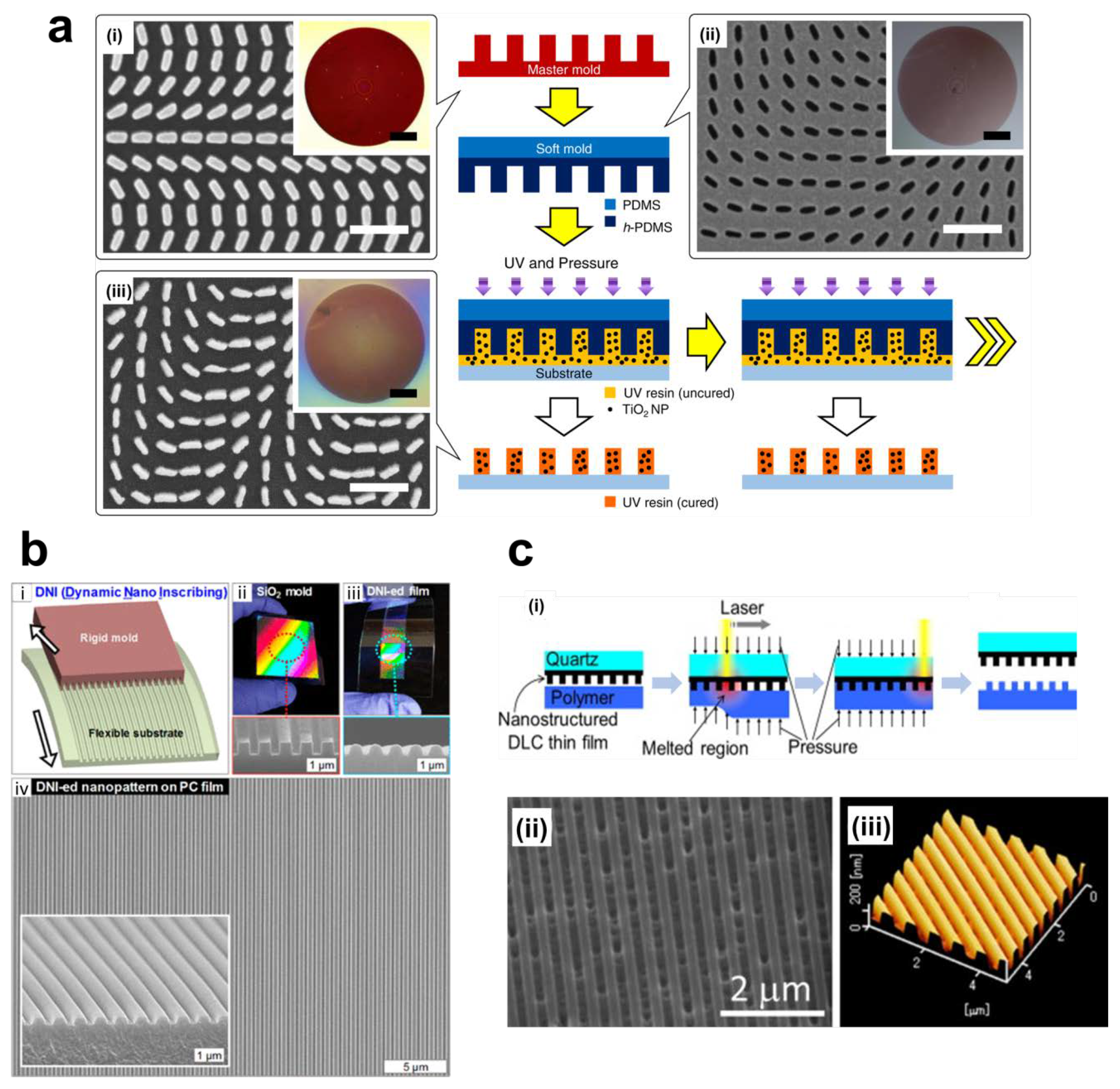
- Ahn, S.H.; Jay Guo, L. Dynamic nanoinscribing for continuous and seamless metal and polymer nanogratings. Nano Lett. 2009, 9, 4392–4397. [Google Scholar] [CrossRef]
- Yokoo, A. Nanoelectrode lithography and multiple patterning. J. Vac. Sci. Technol. B Microelectron. Nanometer Struct. 2003, 21, 2966–2969. [Google Scholar] [CrossRef]
- Schift, H.; Park, S.; Gobrecht, J. Nano-Imprint-Molding Resists for Lithography. J. Photopolym. Sci. Technol. 2003, 16, 435–438. [Google Scholar] [CrossRef][Green Version]
- Chen, S.; Gu, Y.; Lin, J.; Yi, A.; Yi, Z.; Li, J.; Yan, J. Study on vibration-assisted thermal nanoimprint lithography. Appl. Nanosci. 2020, 1–10. [Google Scholar] [CrossRef]
- Atasoy, H.; Vogler, M.; Haatainen, T.; Schleunitz, A.; Jarzabek, D.; Schift, H.; Reuther, F.; Gruetzner, G.; Rymuza, Z. Novel thermoplastic polymers with improved release properties for thermal NIL. Microelectron. Eng. 2011, 88, 1902–1905. [Google Scholar] [CrossRef]
- Slyngborg, M.; Tsao, Y.C.; Fojan, P. Large-scale fabrication of achiral plasmonic metamaterials with giant chiroptical response. Beilstein J. Nanotechnol. 2016, 7, 914–925. [Google Scholar] [CrossRef]
- Schleunitz, A.; Guzenko, V.A.; Messerschmidt, M.; Atasoy, H.; Kirchner, R.; Schift, H. Novel 3D micro- and nanofabrication method using thermally activated selective topography equilibration (TASTE) of polymers. Nano Converg. 2014, 1, 1–8. [Google Scholar] [CrossRef]
- Bender, M.; Fuchs, A.; Plachetka, U.; Kurz, H. Status and prospects of UV-Nanoimprint technology. Microelectron. Eng. 2006, 83, 827–830. [Google Scholar] [CrossRef]
- Fuchs, A.; Vratzov, B.; Wahlbrink, T.; Georgiev, Y.; Kurz, H. Interferometric in situ alignment for UV-based nanoimprint. J. Vac. Sci. Technol. B Microelectron. Nanometer Struct. 2004, 22, 3242–3245. [Google Scholar] [CrossRef]
- Ok, J.G.; Shin, Y.J.; Park, H.J.; Guo, L.J. A step toward next-generation nanoimprint lithography: Extending productivity and applicability. Appl. Phys. A Mater. Sci. Process. 2015, 121, 343–356. [Google Scholar] [CrossRef]
- Chen, Y. Applications of nanoimprint lithography/hot embossing: A review. Appl. Phys. A Mater. Sci. Process. 2015, 121, 451–465. [Google Scholar] [CrossRef]
- Costner, E.A.; Lin, M.W.; Jen, W.-L.; Willson, C.G. Nanoimprint Lithography Materials Development for Semiconductor Device Fabrication. Annu. Rev. Mater. Res. 2009, 39, 155–180. [Google Scholar] [CrossRef]
- Austin, M.D.; Zhang, W.; Ge, H.; Wasserman, D.; Lyon, S.A.; Chou, S.Y. 6 Nm Half-Pitch Lines and 0.04 Νm 2 Static Random Access Memory Patterns By Nanoimprint Lithography. Nanotechnology 2005, 16, 1058–1061. [Google Scholar] [CrossRef]
- Tormen, M.; Carpentiero, A.; Ferrari, E.; Cojoc, D.; Fabrizio, E. Di Novel fabrication method for three-dimensional nanostructuring: An application to micro-optics. Nanotechnology 2007, 18, 385301. [Google Scholar] [CrossRef]
- Saive, R.; Bukowsky, C.R.; Atwater, H.A. Three-dimensional nanoimprint lithography using two-photon lithography master samples. arXiv 2017, arXiv:1602.07261. [Google Scholar]
- Waid, S.; Wanzenboeck, H.D.; Muehlberger, M.; Bertagnolli, E. Optimization of 3D patterning by Ga implantation and reactive ion etching (RIE) for nanoimprint lithography (NIL) stamp fabrication. Microelectron. Eng. 2012, 97, 105–108. [Google Scholar] [CrossRef]
- Yao, Y.; Liu, H.; Wang, Y.; Li, Y.; Song, B.; Bratkovsk, A.; Wang, S.Y.; Wu, W. Nanoimprint lithography: An enabling technology for nanophotonics. Appl. Phys. A Mater. Sci. Process. 2015, 121, 327–333. [Google Scholar] [CrossRef]
- Wiley, B.J.; Qin, D.; Xia, Y. Nanofabrication at high throughput and low cost. ACS Nano 2010, 4, 3554–3559. [Google Scholar] [CrossRef]
- Kim, E.; Wang, F.; Wu, W.; Yu, Z.; Shen, Y.R. Nonlinear optical spectroscopy of photonic metamaterials. Phys. Rev. B-Condens. Matter Mater. Phys. 2008, 78, 2–5. [Google Scholar] [CrossRef]
- Layers, S.; Bergmair, I.; Dastmalchi, B.; Bergmair, M.; Saeed, A.; Hilber, W.; Hesser, G.; Helgert, C.; Pshenay-Severin, E.; Pertsch, T.; et al. Single and multilayer metamaterials fabricated by nanoimprint lithography. Nanotechnology 2011, 22. [Google Scholar] [CrossRef]
- Gao, L.; Shigeta, K.; Vazquez-Guardado, A.; Progler, C.J.; Bogart, G.R.; Rogers, J.A.; Chanda, D. Nanoimprinting techniques for large-area three-dimensional negative index metamaterials with operation in the visible and telecom bands. ACS Nano 2014, 8, 5535–5542. [Google Scholar] [CrossRef]
- Perret, C. Characterization of 8-in. wafers printed by nanoimprint lithography. Microelectron. Eng. 2004, 73, 172–177. [Google Scholar] [CrossRef]
- Lim, H.; Choi, K.B.; Kim, G.; Park, S.; Ryu, J.; Lee, J. Roller nanoimprint lithography for flexible electronic devices of a sub-micron scale. Microelectron. Eng. 2011, 88, 2017–2020. [Google Scholar] [CrossRef]
- Song, J.H.; Lee, H.J.; Lan, S.; Lee, N.K.; Lee, G.A.; Lee, T.J.; Choi, S.; Bae, S.M. Development of the roll type incremental micro pattern imprint system for large area pattern replication. IFIP Adv. Inf. Commun. Technol. 2010, 315, 97–104. [Google Scholar] [CrossRef]
- Tan, H.; Gilbertson, A.; Chou, S.Y. Roller nanoimprint lithography. J. Vac. Sci. Technol. B Microelectron. Nanometer Struct. 1998, 16, 3926–3928. [Google Scholar] [CrossRef]
- Park, S.Y.; Choi, K.B.; Kim, G.H.; Lee, J.J. Nanoscale patterning with the double-layered soft cylindrical stamps by means of UV-nanoimprint lithography. Microelectron. Eng. 2009, 86, 604–607. [Google Scholar] [CrossRef]
- Koo, S.; Lee, S.H.; Kim, J.D.; Hong, J.G.; Baac, H.W.; Kwak, M.K.; Ok, J.G. Controlled airbrush coating of polymer resists in Roll-to-Roll nanoimprinting with regimented residual layer thickness. Int. J. Precis. Eng. Manuf. 2016, 17, 943–947. [Google Scholar] [CrossRef]
- Lee, J.H.; Na, M.; Kim, J.; Yoo, K.; Park, J.; Kim, J.D.J.; Oh, D.K.; Lee, S.; Youn, H.; Kwak, M.K.; et al. Rapid and conformal coating of polymer resins by airbrushing for continuous and high-speed roll-to-roll nanopatterning: Parametric quality controls and extended applications. Nano Converg. 2017, 4, 2–6. [Google Scholar] [CrossRef]
- Frenkel, R.; Kim, B.; Yao, D. Extrusion roller imprinting with a variotherm belt mold. Machines 2014, 2, 299–311. [Google Scholar] [CrossRef]
- Mäkelä, T.; Haatainen, T.; Majander, P.; Ahopelto, J. Continuous roll to roll nanoimprinting of inherently conducting polyaniline. Microelectron. Eng. 2007, 84, 877–879. [Google Scholar] [CrossRef]
- Nagato, K.; Sugimoto, S.; Hamaguchi, T.; Nakao, M. Iterative roller imprint of multilayered nanostructures. Microelectron. Eng. 2010, 87, 1543–1545. [Google Scholar] [CrossRef]
- Dumond, J.J.; Yee Low, H. Recent developments and design challenges in continuous roller micro- and nanoimprinting. J. Vac. Sci. Technol. B Nanotechnol. Microelectron. Mater. Process. Meas. Phenom. 2012, 30, 010801. [Google Scholar] [CrossRef]
- Ahn, S.H.; Guo, L.J. High-speed roll-to-roll nanoimprint lithography on flexible plastic substrates. Adv. Mater. 2008, 20, 2044–2049. [Google Scholar] [CrossRef]
- Ok, J.G.; Park, H.J.; Kwak, M.K.; Pina-Hernandez, C.A.; Ahn, S.H.; Guo, L.J. Continuous patterning of nanogratings by nanochannel-guided lithography on liquid resists. Adv. Mater. 2011, 23, 4444–4448. [Google Scholar] [CrossRef]
- Wang, Y.; Zhang, X. Scale-up of the manufacturing of optical metamaterials. NPG Asia Mater. 2014, 6, 4057. [Google Scholar] [CrossRef][Green Version]
- Ok, J.G.; Youn, H.S.; Kwak, M.K.; Lee, K.T.; Shin, Y.J.; Guo, L.J.; Greenwald, A.; Liu, Y. Continuous and scalable fabrication of flexible metamaterial films via roll-to-roll nanoimprint process for broadband plasmonic infrared filters. Appl. Phys. Lett. 2012, 101, 223102. [Google Scholar] [CrossRef]
- Rai, P.; Oh, S.; Ramasamy, M.; Varadan, V.K. Photonic nanometer scale metamaterials and nanoporous thermoelectric materials for enhancement of hybrid photovoltaic thermoelectric devices. Microelectron. Eng. 2015, 148, 104–109. [Google Scholar] [CrossRef]
- Murthy, S.; Pranov, H.; Feidenhans’L, N.A.; Madsen, J.S.; Hansen, P.E.; Pedersen, H.C.; Taboryski, R. Plasmonic color metasurfaces fabricated by a high speed roll-to-roll method. Nanoscale 2017, 9, 14280–14287. [Google Scholar] [CrossRef]
- Weibel, D.B.; DiLuzio, W.R.; Whitesides, G.M. Microfabrication meets microbiology. Nat. Rev. Microbiol. 2007, 5, 209–218. [Google Scholar] [CrossRef]
- Si, S.; Hoffmann, M. Consecutive imprinting performance of large area UV nanoimprint lithography using Bi-layer soft stamps in ambient atmosphere. Microelectron. Eng. 2017, 176, 62–70. [Google Scholar] [CrossRef]
- Bhingardive, V.; Menahem, L.; Schvartzman, M. Soft thermal nanoimprint lithography using a nanocomposite mold. Nano Res. 2018, 11, 2705–2714. [Google Scholar] [CrossRef]
- Sreenivasan, S.V.; Sreenivasan, V.S. Nanoscale manufacturing enabled by imprint lithography. MRS Bull. 2008, 33, 854–863. [Google Scholar] [CrossRef]
- Cattoni, A.; Chen, J.; Decanini, D.; Shi, J.; Haghiri-Gosnet, A.-M. Soft UV Nanoimprint Lithography: A Versatile Tool for Nanostructuration at the 20nm Scale. In Recent Advances in Nanofabrication Techniques and Applications; InTech: London, UK, 2011; pp. 139–156. [Google Scholar]
- Wi, J.-S.; Lee, S.; Lee, S.H.; Oh, D.K.; Lee, K.-T.; Park, I.; Kwak, M.K.; Ok, J.G. Facile three-dimensional nanoarchitecturing of double-bent gold strips on roll-to-roll nanoimprinted transparent nanogratings for flexible and scalable plasmonic sensors. Nanoscale 2017, 9, 1398–1402. [Google Scholar] [CrossRef] [PubMed]
- Wi, J.-S.; Oh, D.K.; Kwak, M.K.; Ok, J.G. Size-dependent detection sensitivity of spherical particles sitting on a double-bent gold strip array. Opt. Mater. Express 2018, 8, 1774. [Google Scholar] [CrossRef]
- Checcucci, S.; Bottein, T.; Gurioli, M.; Favre, L.; Grosso, D.; Abbarchi, M. Multifunctional Metasurfaces Based on Direct Nanoimprint of Titania Sol–Gel Coatings. Adv. Opt. Mater. 2019, 7, 1–9. [Google Scholar] [CrossRef]
- Bottein, T.; Wood, T.; David, T.; Claude, J.B.; Favre, L.; Berbézier, I.; Ronda, A.; Abbarchi, M.; Grosso, D. “Black” Titania Coatings Composed of Sol-Gel Imprinted Mie Resonators Arrays. Adv. Funct. Mater. 2017, 27, 1604924. [Google Scholar] [CrossRef]
- Garcia, R.; Knoll, A.W.; Riedo, E. Advanced scanning probe lithography. Nat. Nanotechnol. 2014, 9, 577–587. [Google Scholar] [CrossRef]
- Paul, P.C.; Knoll, A.W.; Holzner, F.; Despont, M.; Duerig, U. Rapid turnaround scanning probe nanolithography. Nanotechnology 2011, 22, 275306. [Google Scholar] [CrossRef]
- Oh, D.K.; Lee, S.; Lee, S.H.; Lee, W.; Yeon, G.; Lee, N.; Han, K.S.; Jung, S.; Kim, D.H.; Lee, D.Y.; et al. Tailored Nanopatterning by Controlled Continuous Nanoinscribing with Tunable Shape, Depth, and Dimension. ACS Nano 2019, 13, 11194–11202. [Google Scholar] [CrossRef]
- Ahn, S.H.; Ok, J.G.; Kwak, M.K.; Lee, K.T.; Lee, J.Y.; Guo, L.J. Template-free vibrational indentation patterning (VIP) of micro/nanometer-scale grating structures with real-time pitch and angle tunability. Adv. Funct. Mater. 2013, 23, 4739–4744. [Google Scholar] [CrossRef]
- Ok, J.G.; Panday, A.; Lee, T.; Guo, L.J. Continuous fabrication of scalable 2-dimensional (2D) micro- and nanostructures by sequential 1D mechanical patterning processes. Nanoscale 2014, 6, 14636–14642. [Google Scholar] [CrossRef]
- Ok, J.G.; Ahn, S.H.; Kwak, M.K.; Guo, L.J. Continuous and high-throughput nanopatterning methodologies based on mechanical deformation. J. Mater. Chem. C 2013, 1, 7681–7691. [Google Scholar] [CrossRef]
- Oh, D.K.; Nguyen, D.T.; Lee, S.; Ko, P.; Heo, G.S.; Yun, C.H.; Ha, T.W.; Youn, H.; Ok, J.G. Facile and Scalable Fabrication of Flexible Reattachable Ionomer Nanopatterns by Continuous Multidimensional Nanoinscribing and Low-temperature Roll Imprinting. ACS Appl. Mater. Interfaces 2019, 11, 12070–12076. [Google Scholar] [CrossRef] [PubMed]
- Chou, S.Y.; Keimel, C.; Gu, J. Ultrafast and direct imprint of nanostructures in silicon. Nature 2002, 417, 835–837. [Google Scholar] [CrossRef]
- Cui, B.; Wu, L.; Chou, S.Y. Fabrication of high aspect ratio metal nanotips by nanosecond pulse laser melting. Nanotechnology 2008, 19, 345303. [Google Scholar] [CrossRef][Green Version]
- Nagato, K.; Takahashi, K.; Sato, T.; Choi, J.; Hamaguchi, T. Laser-assisted replication of large-area nanostructures. J. Mater. Process. Tech. 2014, 214, 2444–2449. [Google Scholar] [CrossRef]
- Scaffaro, R.; Shim, E.; Hahn, H. Reliability and Fabrication of Molds for Nanoimprinting. Curr. Nanosci. 2010, 6, 1–11. [Google Scholar] [CrossRef]
- Jeong, H.; Yang, Y.; Cho, H.; Badloe, T.; Kim, I.; Ma, R.-M.; Rho, J. Emerging advanced metasurfaces: Alternatives to conventional bulk optical devices. Microelectron. Eng. 2020, 220, 111146. [Google Scholar] [CrossRef]
- So, S.; Badloe, T.; Noh, J.; Bravo-Abad, J.; Rho, J. Deep learning enabled inverse design in nanophotonics. Nanophotonics 2020, 9, 1041–1057. [Google Scholar] [CrossRef]
- Badloe, T.; Kim, I.; Rho, J. Biomimetic ultra-broadband perfect absorbers optimised with reinforcement learning. Phys. Chem. Chem. Phys. 2020, 22, 2337–2342. [Google Scholar] [CrossRef]
- Sajedian, I.; Lee, H.; Rho, J. Design of high transmission color filters for solar cells directed by deep Q-learning. Sol. Energy 2020, 195, 670–676. [Google Scholar] [CrossRef]
- Sajedian, I.; Rho, J. Accurate and instant frequency estimation from noisy sinusoidal waves by deep learning. Nano Converg. 2019, 6, 27. [Google Scholar] [CrossRef] [PubMed]
- Sajedian, I.; Lee, H.; Rho, J. Double-deep Q-learning to increase the efficiency of metasurface holograms. Sci. Rep. 2019, 9, 1–8. [Google Scholar] [CrossRef] [PubMed]
- So, S.; Mun, J.; Rho, J. Simultaneous Inverse Design of Materials and Structures via Deep Learning: Demonstration of Dipole Resonance Engineering Using Core–Shell Nanoparticles. ACS Appl. Mater. Interfaces 2019, 11, 24264–24268. [Google Scholar] [CrossRef] [PubMed]
- Sajedian, I.; Badloe, T.; Rho, J. Optimisation of colour generation from dielectric nanostructures using reinforcement learning. Opt. Express 2019, 27, 5874–5883. [Google Scholar] [CrossRef]
- So, S.; Rho, J. Designing nanophotonic structures using conditional deep convolutional generative adversarial networks. Nanophotonics 2019, 8, 1255–1261. [Google Scholar] [CrossRef]


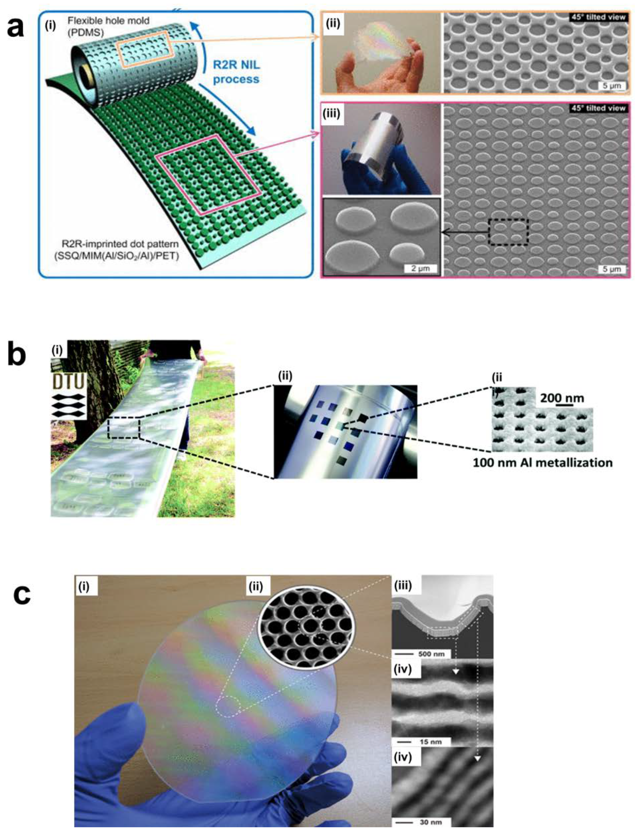
| Comparing Features | Thermal NIL | UV NIL |
|---|---|---|
| Material viscosity | High viscosity in low temperature Low viscosity in high temperature | 1 to 100 cP (general material) |
| Pattern size | Hundred nanometers | <10 nm is possible |
| Resist coating | Spin-on | Spin-on or drop on demand |
| Processing time | Slow due to heating and cooling | Fast |
| Filling driven force | Pressure | Pressure and capillary |
| Type of materials | More material are possible | Material options are limited |
| Plate-to-Plate Type NIL | Roller-Based NIL | ||
|---|---|---|---|
| Roll-to-Plate NIL | Roll-to-Roll NIL | ||
| Mask and substrate | Flat molds (rigid or flexible) with rigid substrate | Roller mold (flexible) with rigid substrate | Roller (rigid or flexible) mold with |
| Printing area | 450 mm 500 mm | 1 m 0.3 m | 300 mm(width) |
| Resolution | Sub-20 nm | 40 nm | Sub-30 nm |
| Throughput | Moderate | High | Very high |
| Contact mechanism | Surface contact | Line contact | Line contact |
| Limitation | High pressure, large-area demolding | Conformal contact | Roller mold fabrication, coating method |
© 2020 by the authors. Licensee MDPI, Basel, Switzerland. This article is an open access article distributed under the terms and conditions of the Creative Commons Attribution (CC BY) license (http://creativecommons.org/licenses/by/4.0/).
Share and Cite
Lee, T.; Lee, C.; Oh, D.K.; Badloe, T.; Ok, J.G.; Rho, J. Scalable and High-Throughput Top-Down Manufacturing of Optical Metasurfaces. Sensors 2020, 20, 4108. https://doi.org/10.3390/s20154108
Lee T, Lee C, Oh DK, Badloe T, Ok JG, Rho J. Scalable and High-Throughput Top-Down Manufacturing of Optical Metasurfaces. Sensors. 2020; 20(15):4108. https://doi.org/10.3390/s20154108
Chicago/Turabian StyleLee, Taejun, Chihun Lee, Dong Kyo Oh, Trevon Badloe, Jong G. Ok, and Junsuk Rho. 2020. "Scalable and High-Throughput Top-Down Manufacturing of Optical Metasurfaces" Sensors 20, no. 15: 4108. https://doi.org/10.3390/s20154108
APA StyleLee, T., Lee, C., Oh, D. K., Badloe, T., Ok, J. G., & Rho, J. (2020). Scalable and High-Throughput Top-Down Manufacturing of Optical Metasurfaces. Sensors, 20(15), 4108. https://doi.org/10.3390/s20154108