Abstract
Galinobisuitite thin films of (Bi2S3)(PbS) were prepared using the chemical bath deposition technique (CBD). Thin films were prepared by a modified chemical deposition process by allowing the triethanolamine (TEA) complex of Bi3+ and Pb2+ to react with S2− ions, which are released slowly by the dissociation of the thiourea (TU) solution. The films are polycrystalline and the average crystallite size is 35 nm. The composition of the films was measured using the atomic absorption spectroscopy (AAS) technique. The films are very adherent to the substrates. The crystal structure of Galinobisuitite thin films was calculated by using the X-ray diffraction (XRD) technique. The surface morphology and roughness of the films were studied using scanning electron microscopes (SEM), transmission electron microscopes (TEM) and stylus profilers respectively. The optical band gaps of the films were estimated from optical measurements.
1. Introduction
Groups IV–VI and V–VI compounds are of continuing interest for many potential and actual applications in heterojunctions, solar cells, photo detectors, thermoelectric devices, photo electrochemical devices, and IR detectors. Bismuthinite and Galena in the form of thin films are promising materials for photoelectronic devices and IR detectors as their energy band gap is between 1.92 and 0.4 eV [1,2]. Direct band gap semiconductors with band gaps in the range 1.2 to 1.7 eV are well suited to convert light into electricity. In this respect, Galinobisuitite (Bi2S3)(PbS) seems to be a promising material.
In the present work, the most favorable results are obtained with thin films of Galinobisuitite (Bi2S3)(PbS) formed by the chemical bath deposition (CBD) method. Capping agents stabilize the nanoparticles and prevent them from aggregating. Polymers are good stabilizing agents because they can cover a larger surface area of the nanoparticles. The optical band gap values of nanoparticles are changed by increasing the molar concentration of the capping agent. These values exhibit a blueshift in Eg, which is related to the decrease in the size of the particles and to the nanoparticles reaching the quantum confinement limit, the emission spectra of semiconductors strongly depend on the energy band structure of the material. The dependence of the band gap and its tuning, which relies on the size of the nanoparticles (quantum dots) and on the carrier concentrations, is important because of its surprising electronic, optical, and physical properties [3,4]. The structural, morphological, and optical properties of the Bi–Pb–S system were investigated, since various compositions between the stable Bi2S3 and PbS phases can be obtained. The differences in the crystallographic structure (orthorhombic for Bi2S3 and cubic for PbS) and the absorption edges (in the visible region for Bi2S3 and near infrared for PbS) constitute a sufficient argument to promote structural and optical investigations [5]. The material obtained was characterized by X-ray diffraction (XRD) and optical measurements, and the results are discussed in connection with the crystal structure of the film. To the best of our knowledge, no report on the structural and optical properties of polycrystalline stoichiometric films of Galinobisuitite (Bi2S3)(PbS), prepared by CBD, has been published.
2. Results and Discussion
2.1. Structural Analysis
Fifteen mineral species were reported having compositions within the (Bi2S3)m(PbS)n system. These lie close to (Bi2S3)(PbS) and are listed together with their reported compositions [6].
2.1.1. Crystal Structure of Bi2S3
Bi2S3 has an orthorhombic lattice with four formula units per unit cell, beyond these, there are three or four additional neighbors at distances that are slightly larger as shown as in Figure 1.
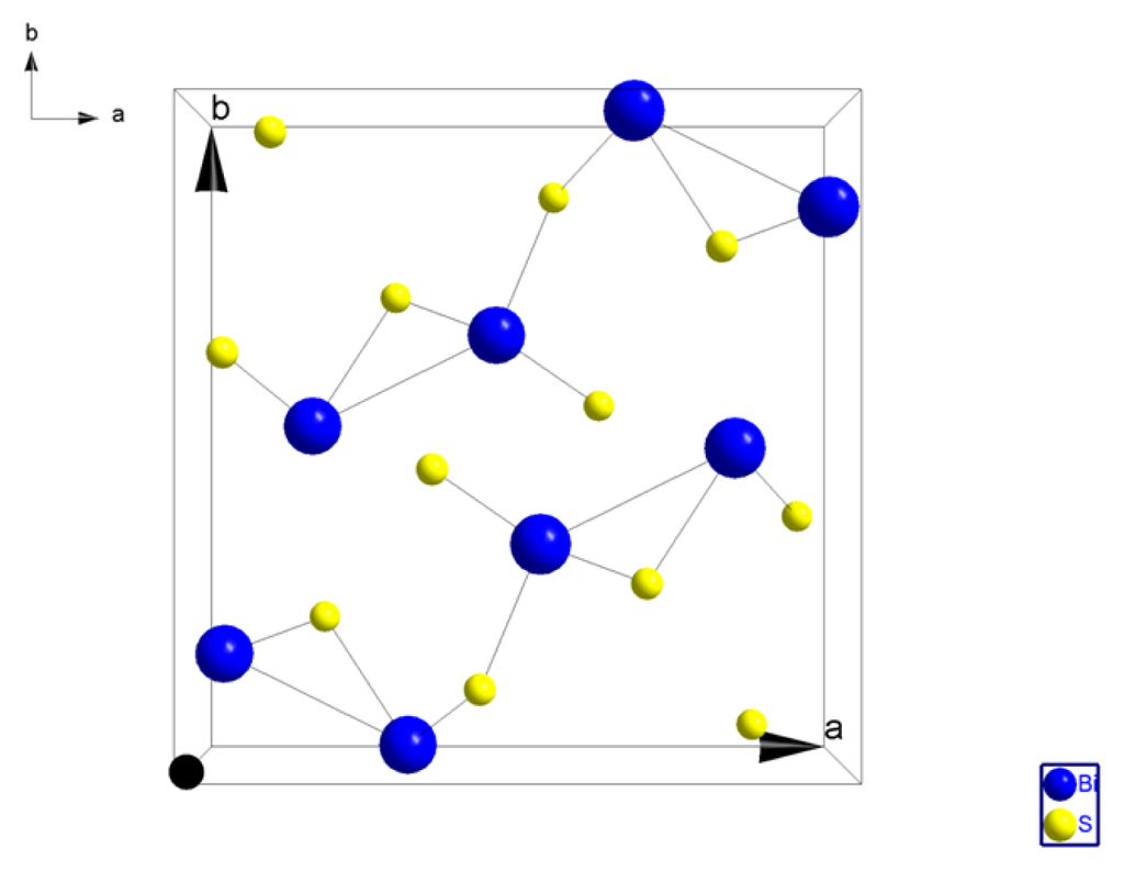
Figure 1.
Structure of (Bi2S3).
This structure can be considered as being made up of puckered sheets or planes of stoichiometric composition perpendicular to the (001) direction. The bonding between these sheets is considerably weaker than that within the sheets [7]. This suggests that cleavage would take place on (010) planes, and crystal growth in the (001) direction, these properties were found to belong these compounds [8].
2.1.2. Crystal Structure of PbS
PbS has a sodium chloride-type structure, with a cubic system; space group (Fm3m) [9]. Noda et al. [10], obtained complete structural information as a function of temperature. Lead Pb is at position (0, 0, 0) and Sulfur S is at (1/2, 1/2, 1/2), as shown in Figure 2.
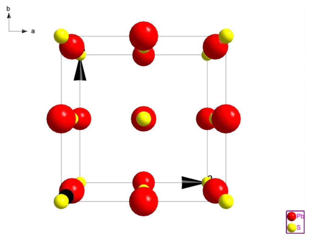
Figure 2.
Structure of (PbS).
2.1.3. Crystal Structure of Galenobismutite (PbS)(Bi2S3)
The crystal structure of Galenobismutite (PbS)(Bi2S3) was studied by several authors [8,10–13]. The lattice constants and space group are summarized in Table 1. The atomic coordinates are summarized in Table 2.

Table 1.
Lattice parameters of (PbS)(Bi2S3): A comparison.
Table 2.
Atomic parameters of Galenobismutite [9].
The structure of the Galinobisuitite (Bi2S3)(PbS) nanoparticulate thin films was calculated with the help of the Fullprof and Chekcell programs. Figure 3 shows the XRD patterns for the (Bi2S3)(PbS) films as-deposited and annealed at 623 K for 1 h, and annealed at 598 K for 4 h. The lattice parameters are illustrated in Table 3, a typical Lebail fit analysis is shown in Figure 4, and the indexing data are illustrated in Table 4. Typical peak matching is shown in Figure 5. Calculated crystal structure of (Bi2S3)(PbS) thin films is shown in Figure 6.
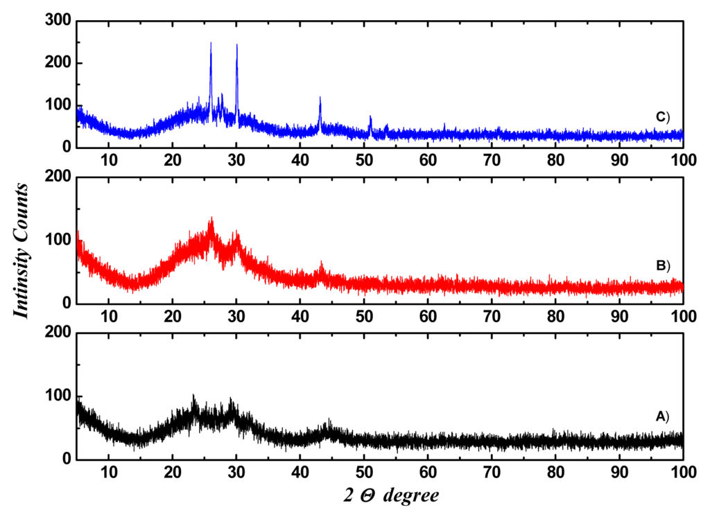
Figure 3.
XRD of (Bi2S3)(PbS) thin films, (A) As-deposited; (B) Annealed at 623 K for 1 h; and (C) Annealed at 698 K for 4 h.
Table 3.
Lattice parameters of (Bi2S3)(PbS).
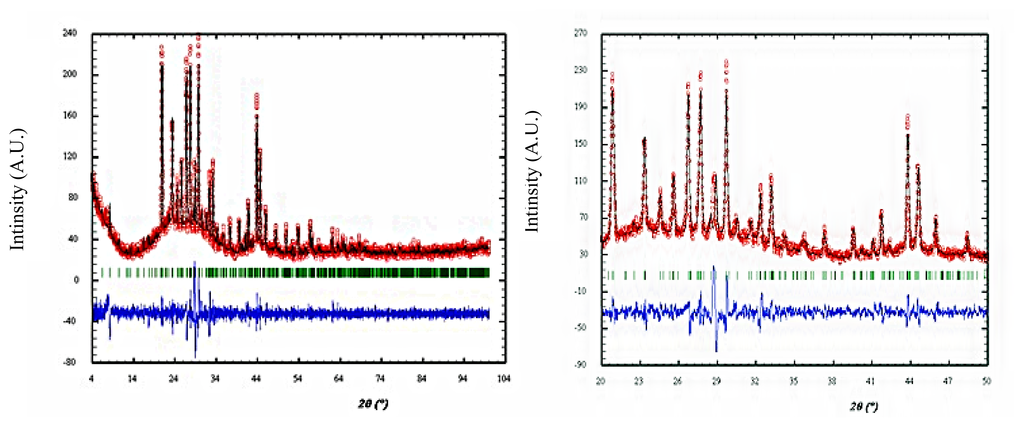
Figure 4.
Lebail fit analysis of (Bi2S3)(PbS) thin films.
Table 4.
Indexing of peaks in (Bi2S3)(PbS).
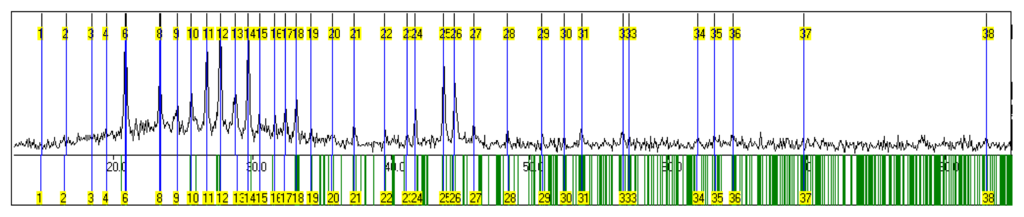
Figure 5.
Measured reflections of (Bi2S3)(PbS) thin films.
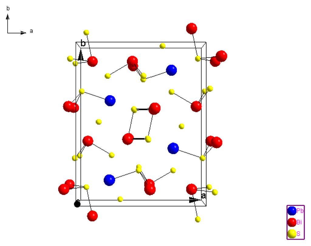
Figure 6.
Structure of (Bi2S3)(PbS) thin films.
2.2. The Surface Morphology Studies
The surface morphology of the (Bi2S3)(PbS) films is sensitive to compositions types, concentrations of the solutions mixtures, pH values, and both of the bath and annealing temperature These factors affect the structural morphology of the films [14]. Figure 7a shows that the small spherical nanograins, approximately 20–40 nm in size, were uniformly distributed over the smooth homogeneous background of the crystalline phase. The small grains are distributed rather distantly from each other, indicating the regular growth rate of the grains. Figure 7b shows the reduced grain density, indicating the noticeably smaller size of the grain. The RMS surface roughness is very slight.
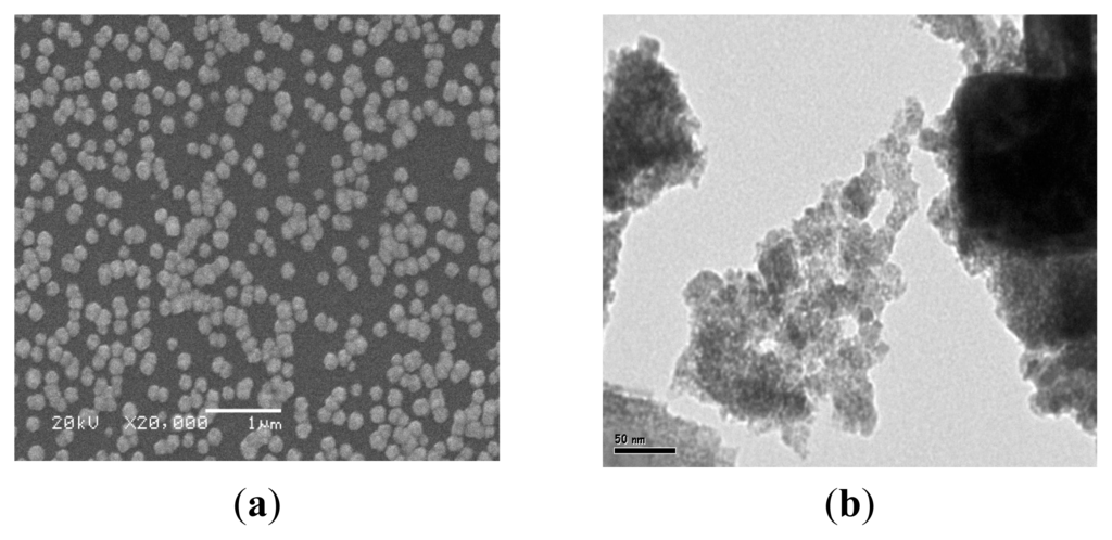
Figure 7.
Surface morphology of (Bi2S3)(PbS) thin films, (a) SEM; (b) TEM.
2.3. The Optical Properties Studies
The typical transmission curves are shown in Figure 8a. The transmission samples showed gradual light absorption in a wide range of optical wavelengths (300–500 nm). The optical absorption edge of the films shifted toward a longer wavelength, which indicates that the optical band gap linearly decreased from 1.92 eV for Bi2S3, to 1.5 eV for Bi2S3 PbS.
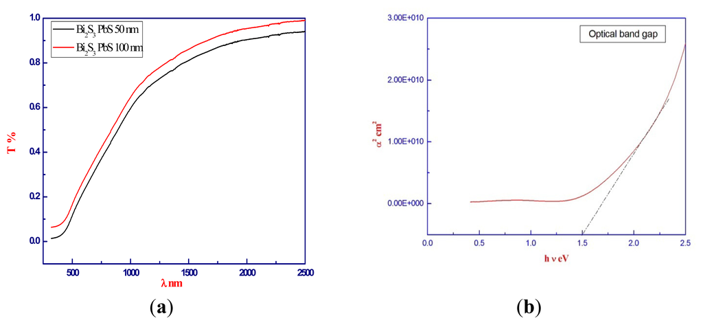
Figure 8.
Optical properties of (Bi2S3)(PbS) thin films, (a) Typical transmission curves; (b) Optical band gap Eg.
Isomura et al. [14] and Susama et al. [15] calculated the optical constants and energy band gap of the films from the measured transmission using the following relation:
where d is the thickness of the films, and T is the transmission.
The optical band gap Eg were obtained from the linear portion of the (α2) vs. (h·ν) plot. An Eg value is obtained through the intersection of the straight line with the axis of the photon energy. In Figure 8b, the plot of (α2) vs. (h·ν) for direct transition of (Bi2S3)(PbS) films is shown. The confinement effect appears as a shift in edge of the absorption spectra and the absorption to lower wavelengths, possibly due to the decrease in the grain size and the decrease in the number of defects. It is clearly seen from the optical spectrum that an absorption edge shift toward a lower wavelength in the films occurs. Due to this effect, the Eg of the material increases as the size of the particle decreases. This property makes it an excellent candidate for opto-electronic applications in many fields, such as photography, IR detectors, solar absorbers, light emitting devices, and solar cells.
3. Experimental Section
3.1. Experimental Procedure
Some authors [8,16,17] reported the synthesis of (PbS)6(Bi2S3), (PbS)3(Bi2S3), (PbS)(Bi2S3), (PbS)2(Bi2S3), and (PbS)4(Bi2S3). They reported three ternary phases, designated as II, III, and IV, of the approximate compositions (PbS)5(Bi2S3), (PbS)3(Bi2S3), and (PbS)(Bi2S3). All these experiments were performed in closed, evacuated silica tubes in which a vapor phase was always present. Galinobisuitite (Bi2S3)(PbS) nanoparticle thin films were deposited on glass substrates (12 × 25 mm2) cleaned with detergent, degreased with trichloroethylene, acetone, and ethanol, rinsed with deionized water in an ultrasonic cleaner, and finally etched in a 10% HF solution immediately before use for the depositions [6]. Galinobisuitite (Bi2S3)(PbS) nanoparticle thin films were deposited from a solution; the chemical deposition bath was prepared according to the following procedures 1 M solution in distilled water, of bismuth nitrate-lead nitrate solution was complexed by the addition of triethanolamine. This was followed by the addition of 1 M thiourea, and 17 M ammonia solution and water. The basic overall reactions are based on Equations (2) and (3):
To stop agglomeration, we used polyvinylpyrrollidone (PVP) as a capping agent after a few minutes of reaction, when the black precipitate was deposited on the glass substrate. The samples and holders were removed from the chemical bath after a deposition time of 60 min. The films obtained by this method, after ultrasonic cleaning, were smooth, uniform, and adherent. XRD measurements were made using Cu Kα radiation of wavelength λ = 0.15406 nm in the scan range 2θ = 4°–100°. Surface morphology was examined using a JEOL model JSM-6380 LA scanning electron microscope (SEM) (JEOL, Musashino, Tokyo, Japan). Surface roughness was measured using a DektakXT advanced system (Bruker, Billerica, MA, USA) with optional isolation pads. The formation of nanoparticles was confirmed using a transmission electron microscope (TEM, JEOL 1010, JEOL, Musashino, Tokyo, Japan). Optical transmission measurements were performed using a UV/VIS Jasco 7800 spectrophotometer (JASCO, Mary’s Court, Easton, PA, USA).
3.2. Measurment of Atomic Absorption
The powder sample (Bi2S3)(PbS) was digested by concentrated nitric acid (HNO3) and lead concentrations were determined according to the standard method [18]. For each analytical run, a calibration curve composed of a blank and three or more standards was within the method’s working range, and a replicate additional standard solution was analyzed after every sample. An external reference standard from Merck (MERCK, Darmstadt, Germany) and quality control samples from U.S.E.P.A (U.S.E.P.A, Washington, DC, USA) we are used to confirm the instrument’s lead concentration reading. The showed a slight difference between the desired and measured ratios of lead.
4. Conclusions
In summary, we prepared Galinobisuitite thin films of (Bi2S3)(PbS) using the chemical bath deposition technique (CBD). The grain size lies in the interval of 20–40 nm. We calculated the lattice parameters, space group, and crystal structure. The surface morphology showed that the small spherical nanograins were uniformly distributed over the smooth homogeneous background of the crystalline phase. Optical absorption spectra were quantified for the Galinobisuitite thin films of (Bi2S3)(PbS), in which the redshift of Eg was associated with the decrease in the average grain size. The direct band gap energy (Eg) was in the range of 1.5 eV.
Acknowledgments
The authors would like to extend their sincere appreciation to the Deanship of Scientific Research at King Saud University for its funding of this research through the research group projects No RGP-VPP-306.
Conflicts of Interest
The authors declare no conflict of interest.
References
- Mahmoud, S.; Eid, A.H.; Omar, H. Optical characteristics of bismuth sulfide (Bi2S3) thin films. Fizika A 1997, 3, 111–120. [Google Scholar]
- Mahmoud, S.; Omar, H. Growth and characterization of lead-sulfide films deposited on glass substrates. Fizika A 2001, 1, 21–30. [Google Scholar]
- Ajji, Z. Grafting of poly(vinyl pyrrolidone) with citric acid using gamma irradiation. Nuclear Instrum. Methods Phys. Res. B 2007, 265, 179–182. [Google Scholar]
- Wang, C.; Shen, E.; Wang, E.; Gao, L. Controllable synthesis of ZnO nanocrystals via a surfactant-assisted alcohol thermal process at a low temperature. Mater. Lett 2005, 59, 2867–2871. [Google Scholar]
- Malika, B.; Noureddine, B.; Mourad, M.; Abdelkader, O.; Attouya, B.; Hind, T.-D. Investigations in structural morphological and optical properties of Bi–Pb–S system thin films. Results Phys 2013, 3, 30–37. [Google Scholar]
- Abd Elkader, O. Preparation and characterization of nanostructured zinc oxide thin films. Proceedings of International Conference on Fundamental and Applied Sciences (ICFAS 2012), Kuala Lumpur, Malaysia, 12–14 June 2012.
- Kupcik, V.; Vesla-Novakova, L. Zur Kristallstruktur des. Bismuthinits Bi2S3. Tschermaks Miner. U. Petrogr. Mitt 1970, 14, 55–59. [Google Scholar]
- Berry, L.G. Studies of mineral sulpho-salts: IV galenobismutite and lillianite. Amer. Min 1940, 25, 726–734. [Google Scholar]
- Yamazaki, T.; Watakabe, Y.; Suzuki, Y.; Nakata, H. A dry etching technique using electronn beam resist-PbS. J. Electrochem. Soc 127.
- Noda, Y.; Ohba, S.; Sato, S.; Saito, Y. Charge distribution and atomic thermal vibration in lead chalcogenide crystals. Acta Crystal. Sect. B 1983, 39, 312–317. [Google Scholar]
- Wickman, F.E. Galenobismutite PbBi2S4. cf. Ag-free lillianite, structure. Ark. Min 1951, 1, 219. [Google Scholar]
- Iitaka, Y.; Nowacki, W. A Redetermination of the crystal structure of galenobismutite, PbBi2S4. Acta Crystallogr 1962, 15, 691–698. [Google Scholar]
- Said, M.S.; Zemel, N.J. Properties of PbS-PbO crystalline films. I. Preparation and physical Structure. J. Appl. Phys 1976, 47, 886–870. [Google Scholar]
- Isomura, S.; Shirakata, S.; Abe, T. Some properties of CuInSe2 films prepared by vacuum evaporation of elements. Solar Energy Mater 1991, 22, 223. [Google Scholar]
- Susama, M.; Padhi, H.C. Preparation and characterization of (Bi2S3)1−x(CdS)x solid solution thin films. J. Appl. Phys 1994, 75, 4576–4580. [Google Scholar]
- Mahmoud, S.; Omar, H. Structure and optical properties of thermally deposited bismuth sulfide-lead sulfide films. J. Appl. Sci. Res 2008, 4, 303–310. [Google Scholar]
- Nieseni, P.T.; de Guire, R.M. Review: Deposition of ceramic thin films at low temperatures from aqueous solutions. J. Electroceram 2001, 6, 169–207. [Google Scholar]
- APHA-AWWA-WPCF, Standard Methods for the Examination of Water and Wastewater, 17th ed.; American Public Health Association: Washington, DC, USA, 1989.
© 2014 by the authors; licensee MDPI, Basel, Switzerland This article is an open access article distributed under the terms and conditions of the Creative Commons Attribution license (http://creativecommons.org/licenses/by/3.0/).