Proceeding Paper

Imaging with Diffractive Axicons Rapidly Milled on Sapphire by Femtosecond Laser Ablation †

1
Optical Sciences Centre and ARC Training Centre in Surface Engineering for Advanced Materials (SEAM), School of Science, Computing and Engineering Technologies, Swinburne University of Technology, Hawthorn, VIC 3122, Australia
2
Institute of Physics, University of Tartu, Ülikooli 18, 50090 Tartu, Estonia
3
World Research Hub Initiative (WRHI), School of Materials and Chemical Technology, Tokyo Institute of Technology, 2-12-1, Ookayama, Meguro-ku, Tokyo 152-8550, Japan
*
Authors to whom correspondence should be addressed.
Presented at the International Conference on “Holography Meets Advanced Manufacturing”, Online, 20–22 February 2023.
Eng. Proc. 2023, 34(1), 26; https://doi.org/10.3390/HMAM2-14147
Published: 13 March 2023

Abstract

:
We show that single-pulse burst fabrication will produce a flatter and smoother profile of axicons milled on sapphire compared to pulse overlapped fabrication which results in a damaged and much rougher surface. The fabrication of large-area (sub-1 cm cross-section) micro-optical components in a short period of time (∼10 min) and with less processing steps is highly desirable and would be cost-effective. Our results were achieved with femtosecond laser fabrication technology which has revolutionized the field of advanced manufacturing. This study compares three configurations of axicons such as the conventional axicon, a photon sieve axicon (PSA) and a sparse PSA directly milled onto a sapphire substrate. Debris of redeposited amorphous sapphire were removed using isopropyl alcohol and potassium hydroxide. A spatially incoherent illumination was used to test the components for imaging applications. Non-linear reconstruction was used for cleaning noisy images generated by the axicons.

1. Introduction

Axicons are diffractive optical elements which have a line focus. Importantly. axicons are Bessel beam generators and can be used for a range of different applications including optical trapping [1,2]. Bessel beams are important as they are diffraction resistant and can be used for optical imaging applications [3] and biomedical applications such as ultrasound imaging [4,5,6]. (Figure 1) shows the lens axicon with its unique large depth of focus (DOF) and Bessel beam generation.
In this body of work, an optimal and record processing time for micro-optical components is described, where the process used has fewer steps and is more cost effective than previous attempts. Instead of using axicon lenses, micro-optical binary surface axicons with a two phase or amplitude configurations are used. The extra configurations give rise to, in total, three different diffractive optical elements: a conventional surface axicon, surface photon sieve axicon (PSA), and sparse surface photon sieve axicon (sparse PSA) which were directly milled onto a sapphire substrate.
This particular micro-optical component falls into the category of diffractive optics and plays an important role in many areas of research; furthermore, they have been manufactured using different techniques. The techniques generally employed are photolithography [7], electron beam lithography [8], and ion beam lithography [9], which are time-consuming and expensive, making the device itself expensive. Femtosecond laser ablation is superior to all of the above methods with only one exception: the ability to deliver a practical solution for large areas such as millimeter-to-centimeter-scale micro-optical element fabrication [10,11,12,13]. Lately, there has been a shift in focus in imaging research from using coherent light sources to incoherent ones due to the many advantages of the latter, such as their broad applicability, low cost, and high resolving power. We have used femtosecond fabrication with ablation to rapidly fabricate two-level axicons directly onto sapphire substrates. Two configurations, conventional ring and sieve configurations, were produced. Furthermore, our work focused on rapid fabrication to manufacture large-area diffractive optical elements for astronomical imaging applications [14].
The beam characteristics were investigated for a spatially incoherent illumination since it is available at low cost and is therefore relevant to large-scale astronomical applications. In astronomy, large area devices are required which can be easily manufactured using femtosecond fabrication systems. The optical configuration of light diffracted from a point object is incident on a diffractive axicon and the intensity distribution is recorded (shown in Figure 2).

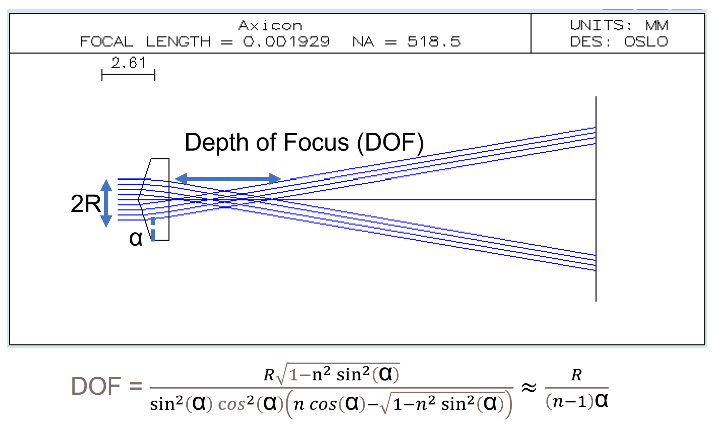
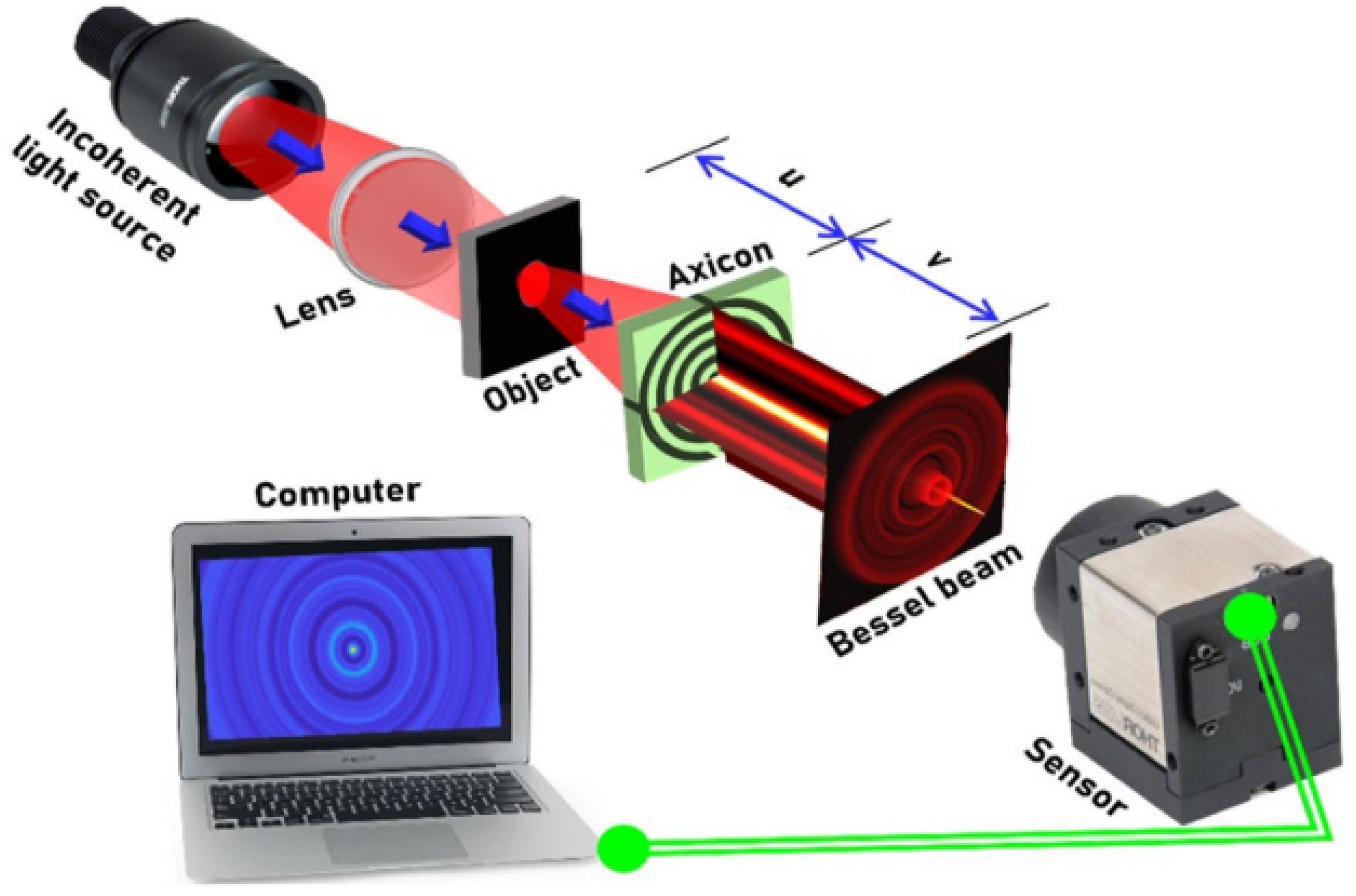
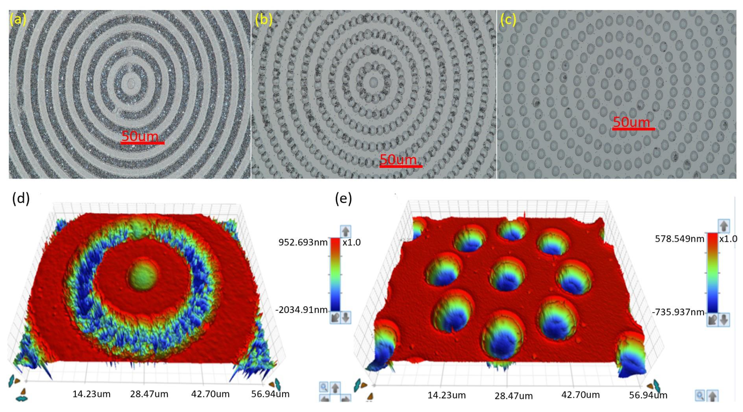
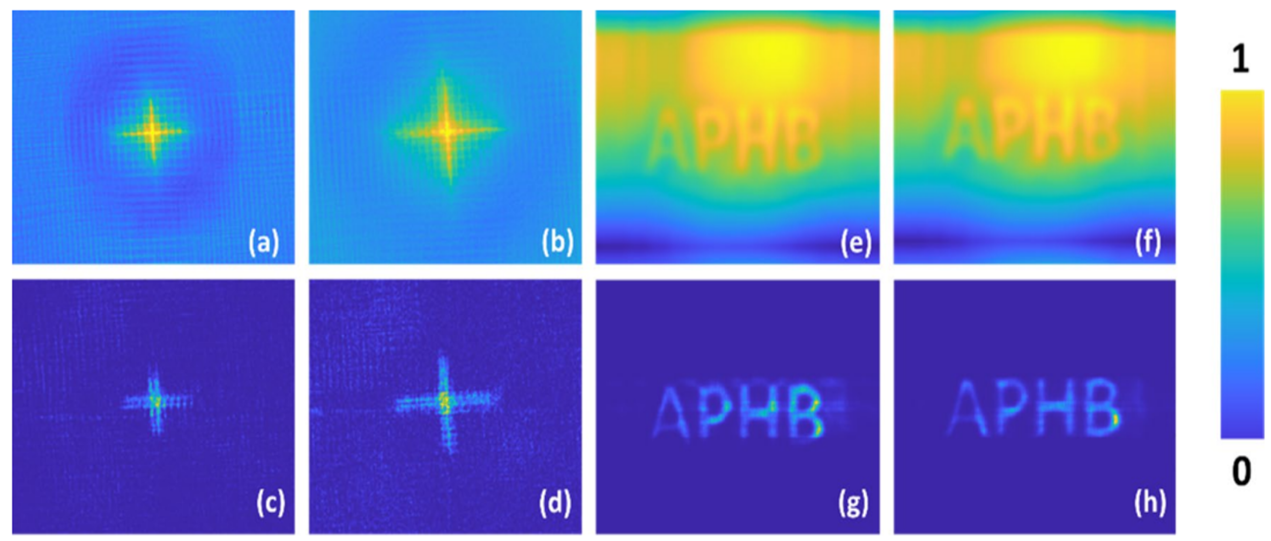
2. Results and Discussion: Laser Ablation and Imaging

2.1. Laser Ablation

The fabrication was carried out on a sapphire substrate of 500 μ min thickness and 10 mm by 10 mm in size. Sapphire has a refractive index of n s a p p h i r e = 1.76 and has a spectral window from 300 nm to 6000 nm. The milling depth, t, is determined by the relationship between the wavelength that the diffractive optical element is desired to interact with and the refractive index of the material ( t = λ / 2 ( n s a p p h i r e 1 ) ). The thickness t was determined to be 400 μ m for λ ≈ 600 nm. The wavelength source for optical testing is 617 nm. Acetone and Iso-Propyl alcohol were used to clean the substrate prior to fabrication.
Three optical devices—a conventional surface axicon, surface photon sieve axicon (PSA), and sparse surface photon sieve axicon (sparse PSA), shown in Figure 3a,b,c respectively—were created using the light conversion PHAROS laser operating at a 200 kHz repetition rate, λ = 1030 nm wavelength, 2.5 W average power, 230 fs pulse duration and a 5× magnification, NA = 0.14 numerical aperture Mitutoyo Plan APO NIR infinity corrected objective lens. Two pulses per ablation spot were used to ablate the regions of the axicon; as a consequence, these more heavily overlapped regions incurred ripple formation. The attenuator serves to create more precise beam energies in combination with the objective lens. Here, a 5 μ J beam was used to achieve the fabrication which led to pulse energies of 70 TW/cm2, even though the ablation threshold of sapphire is only in the order of 10 TW/cm2 and with ablation spots with a diameter of 8.9 μ m.

2.2. Imaging

Optical testing was carried out according to Figure 2 using a high-power LED and a spectral filter to improve the temporal coherence. A pinhole with a size of 100 μ m and a cross shaped object Figure 4a,b were used for imaging. A 3× magnifying system was used to re-image the intensity distribution that is close to the diffractive optical elements on an image sensor. These optical elements were mounted one after the other and the intensity distributions were recorded at 5 mm for the axicon, PSA and sparse PSA. The pinhole was replaced by a cross object and the intensity patterns again were recorded at 3 cm from the DOEs. Again, the images were cleaned using non-linear reconstruction and to further improve the cleaning results, additional filters such as a median filter and correlation filters were used. A significant difference was seen in the cleaned images compared to the original images without filters.

3. Conclusions and Future Works

This study showed that the fabrication time could be cut to 10 min using the femtosecond laser fabrication method for large-area, i.e., 5 mm × 5 mm, objects. It was noticed that the beam overlap during milling resulted in the redeposition of material resulting in a lower depth than the case without beam overlap, which is contrary to the common belief that overall higher exposure with the beam overlap increases the depth. An increase in roughness has been noticed and it is contributed to by the redeposition and light-matter interaction at temperature changes due to the ablation process. It is noted that debris will have to be reduced to avoid a build-up of rough areas. Some of the latest developments in astronomical spectral imaging technologies such as FOBOS require numerous micro-optical devices for the successful implementation of free space to fiber bundle coupling for spectral imaging. The current work shows the possibility of rapid fabrication and beam cleaning capable of retrieving spatial information in addition to the recorded spectral information.

Author Contributions

Conceptualisation, S.J., V.A. and S.H.N.; investigation, D.S., M.H., V.A. and T.K.; writing— original draft preparation, D.S.; review and editing, all authors. All authors have read and agreed to the published version of the manuscript.

Funding

This research was funded by the Australian Research Council, grant number LP190100505. S.J. is grateful for startup funding from the Nanotechnology Facility at Swinburne and to the Workshop-on-Photonics for the technology transfer project, which installed the first industrial grade microfabrication setup in Australia. Part of this study was created during a Grand Challenge undergraduate project of A.T.

Institutional Review Board Statement

Not applicable.

Informed Consent Statement

Not applicable.

Data Availability Statement

The data presented in this study are available on request from the corresponding author.

Conflicts of Interest

The authors declare no conflict of interest.

References

  1. Ding, Z.; Lai, G. Enhancement of axial optical trapping force using a pair of axicons. In Proceedings of the Technical Digest. CLEO/Pacific Rim ’99. Pacific Rim Conference on Lasers and Electro-Optics (Cat. No.99TH8464), Seoul, Republic of Korea, 30 August–3 September 1999; Volume 2, pp. 369–370. [Google Scholar] [CrossRef]
  2. Balasubramani, V.; Vijayakumar, A.; Rai, M.R.; Rosen, J.; Cheng, C.J.; Minin, O.V.; Minin, I.V. Binary square axicon with chiral focusing properties for optical trapping. Opt. Eng. 2019, 59, 041204. [Google Scholar] [CrossRef]
  3. Khonina, S.N.; Kazanskiy, N.L.; Karpeev, S.V.; Butt, M.A. Bessel Beam: Significance and Applications—A Progressive Review. Micromachines 2020, 11, 997. [Google Scholar] [CrossRef] [PubMed]
  4. Hsu, D.K.; Margetan, F.J.; Thompson, D.O. Bessel beam ultrasonic transducer: Fabrication method and experimental results. Appl. Phys. Lett. 1989, 55, 2066–2068. [Google Scholar] [CrossRef]
  5. Lu, J.; Song, T.; Kinnick, R.; Greenleaf, J. In vitro and in vivo real-time imaging with ultrasonic limited diffraction beams. IEEE Trans. Med. Imaging 1993, 12, 819–829. [Google Scholar] [CrossRef] [PubMed]
  6. Lu, J.Y.; Xu, X.L.; Zou, H.; Greenleaf, J. Application of Bessel beam for Doppler velocity estimation. IEEE Trans. Ultrason. Ferroelectr. Freq. Control 1995, 42, 649–662. [Google Scholar] [CrossRef]
  7. Kondo, T.; Juodkazis, S.; Mizeikis, V.; Misawa, H.; Matsuo, S. Holographic lithography of periodic two-and three-dimensional microstructures in photoresist SU-8. Opt. Express 2006, 14, 7943–7953. [Google Scholar] [CrossRef]
  8. Anand, V.; Ng, S.H.; Katkus, T.; Juodkazis, S. White light three-dimensional imaging using a quasi-random lens. Opt. Express 2021, 29, 15551–15563. [Google Scholar] [CrossRef] [PubMed]
  9. Seniutinas, G.; Gervinskas, G.; Anguita, J.; Hakobyan, D.; Brasselet, E.; Juodkazis, S. Nanoproximity direct ion beam writing. Nanofabrication 2016, 2, 6. [Google Scholar] [CrossRef]
  10. Marcinkevǐcius, A.; Juodkazis, S.; Watanabe, M.; Miwa, M.; Matsuo, S.; Misawa, H.; Nishii, J. Femtosecond laser-assisted three-dimensional microfabrication in silica. Opt. Lett. 2001, 26, 277–279. [Google Scholar] [CrossRef] [PubMed]
  11. Malinauskas, M.; Žukauskas, A.; Hasegawa, S.; Hayasaki, Y.; Mizeikis, V.; Buividas, R.; Juodkazis, S. Ultrafast laser processing of materials: From science to industry. Light. Sci. Appl. 2016, 5, 2047–7538. [Google Scholar] [CrossRef] [PubMed]
  12. Juodkazis, S.; Yamasaki, K.; Mizeikis, V.; Matsuo, S.; Misawa, H. Formation of embedded patterns in glasses using femtosecond irradiation. Appl. Phys. A 2004, 4, 1549–1553. [Google Scholar] [CrossRef]
  13. Vanagas, E.; Kudryashov, I.; Tuzhilin, D.; Juodkazis, S.; Matsuo, S.; Misawa, H. Surface nanostructuring of borosilicate glass by femtosecond nJ energy pulses. Appl. Phys. Lett. 2003, 82, 2901–2903. [Google Scholar] [CrossRef]
  14. Smith, D.; Ng, S.H.; Han, M.; Katkus, T.; Anand, V.; Glazebrook, K.; Juodkazis, S. Imaging with diffractive axicons rapidly milled on sapphire by femtosecond laser ablation. Appl. Phys. B 2022, 127, 154. [Google Scholar] [CrossRef]
Figure 1. Conventional axicon lens simulated in OSLO software for application at a wavelength of 550 nm. Depth of focus equation for conventional axicon lens.
Engproc 34 00026 g001
Figure 2. Optical configuration for the generation of Bessel beams by a diffractive axicon. u is the distance from the object being imaged, and v is the distance between the imaging axicon to the sensor. In this case u = v. Reprinted with permissions from Ref. [14]. Copyright 2022 Applied Physics B.
Engproc 34 00026 g002
Figure 3. Optical microscope images of the three different devices created: a conventional surface axicon (a), surface photon sieve axicon (PSA) (b), and sparse surface photon sieve axicon (sparse PSA) (c). Below we provide the optical profilometer images of the conventional surface axicon (d) and sparse surface photon sieve axicon (sparse PSA) (e). Reprinted with permissions from Ref. [14]. Copyright 2022 Applied Physics B.
Engproc 34 00026 g003
Figure 4. Intensity distribution of cross object recorded at (a) z = 5 cm and (b) z = 6 cm and the corresponding cleaned images (c) z = 5 cm and (d) z = 6 cm, respectively. Intensity distribution of synthetic object ‘APHB’ recorded at (e) z = 5 cm and sparse (f) z = 6 cm and the corresponding cleaned images (g) z = 5 cm and (h) z = 6 cm, respectively. Reprinted with permissions from Ref. [14]. Copyright 2022 Applied Physics B.
Engproc 34 00026 g004
Disclaimer/Publisher’s Note: The statements, opinions and data contained in all publications are solely those of the individual author(s) and contributor(s) and not of MDPI and/or the editor(s). MDPI and/or the editor(s) disclaim responsibility for any injury to people or property resulting from any ideas, methods, instructions or products referred to in the content.

