Abstract
Additive manufacturing offers several advantages, such as rapid prototyping, cost-efficient production, and flexibility in constructing components. This work presents the design and fabrication of a strain sensor capable of generating electrical signals under applied mechanical loads, enabling potential failure prediction. The sensor was manufactured using the Fused Deposition Modeling 3D-printing process, combining acrylonitrile-styrene-acrylate as structural and protective layers with a conductive polylactic acid matrix containing carbon nanotubes as the sensing element. To assess its performance, the sensor was embedded within a Glass Fiber-Reinforced Polyester composite and subjected to bending tests. The results demonstrate a reliable sensing response, characterized by a measurable increase in electrical resistance under bending load. Moreover, the change in resistance increased with applied bending force, demonstrating the sensor’s feasibility for structural health monitoring applications.
1. Introduction
The utilization of additive manufacturing (AM) for fabricating strain sensors has grown significantly in recent years, driven by technological advances that have made 3D printing platforms affordable, versatile, and accessible for both research and industrial applications [1,2,3]. Techniques such as fused deposition modeling (FDM), stereolithography (SLA), selective laser sintering (SLS), and direct ink writing (DIW) enable the production of sensors with tailored mechanical and electrical properties, rapid prototyping, and the integration of functional materials into complex architectures [1,4]. The process of layer-by-layer deposition provides precise control over material distribution, facilitating structural optimization, multifunctionality, and the fabrication of diverse sensing components, while reducing material waste. Fabrication of sensors through AM eliminates the need for specialized machinery and tools. Printed electronics offer high adaptability to application-specific requirements, alongside excellent performance. Typical examples include printed resistors, capacitors, antennas, inductors, transistors, thin-film diodes, sensors, and other electronic components [2]. AM has been successfully applied to fabricate force sensors, acoustic and ultrasonic sensors, optical sensors, electromagnetic sensors, bio- and chemo-sensors, as well as flow sensors, demonstrating its versatility across a wide range of sensing applications [1]. The development of strain sensors using thermoplastic polymers incorporating carbon particles or other conductive microstructures has been an issue of great interest in recent years [5,6].
In general, a sensor is a device that responds to changes in its environment and conveys them through measurable electrical signals for monitoring or processing; strain sensors transduce mechanical deformation into electrical signals [7] while piezoresistive sensors respond to mechanical stress by a change in their resistance; they typically consist of a deformable conductive material deposited on or embedded within an inactive stretchable material [5]. Common conductive materials include graphene, conductive nanoparticles, and Carbon Nanotubes (CNTs) [1,6]. Strain sensors can be fabricated using AM techniques such as Fused Deposition Modeling (FDM) or Digital Light Processing (DLP). In FDM, a polymer filament enriched with CNTs or other conductive additives, is heated and extruded through a precision nozzle. The thermoplastic filament—commonly used materials include PLA, ABS, or PC—can be employed either in its pure form or enriched with appropriate conductive additive such as carbon nanotubes (CNTs), graphene, or carbon black to impart electrical functionality [5,6,7]. The sensor structure is constructed layer by layer onto a build platform according to the predefined toolpaths generated during the slicing process. The resolution of FDM printing is determined by several parameters depending on the desired balance between printing accuracy and speed. The extrusion temperature must be carefully controlled to ensure proper filament flow and interlayer adhesion, while avoiding thermal degradation of the polymer or conductive filler. One advantage of FDM in the fabrication of strain sensors is the ability to directly print complex geometries with embedded conductive pathways, eliminating the need for post-processing steps. However, the anisotropic nature of FDM parts, arising from the layer-by-layer deposition process, can influence both the mechanical properties and the electrical response of the sensor. Optimizing printing parameters—such as infill density, raster orientation, and layer height—is therefore crucial for achieving reliable sensor performance.
2. Methods and Materials
The process of creating the sensor presented in this work involves four stages: (i) design of the sensor parts, (ii) fabrication of the parts by FDM, (iii) thermal treatment (annealing) of the printed sensor to stabilize its performance, and (iv) incorporation of the sensor unit into a Glass Fiber Reinforced Polyester (GFRP) composite.
Stage (i) consisted of designing the sensor geometry in Rhinoceros® software (Rhinoceros 3D, Version 5.0. Robert McNeel & Associates) [8] and exporting it in StereoLithography (STL) format, which was subsequently imported into Ultimaker Cura® (version 4.11.0) for slicing and toolpath generation. The resulting geometry and dimensions of the main parts of the sensor are presented in Figure 1.
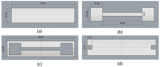
Figure 1.
Component drawings of the strain sensor assembly; dimensions are given in millimeters (mm): (a) non-conductive substrate (ASA); (b) conductive piezoresistor (CNT-enriched PLA); (c) filling material (ASA); (d) protective layer (ASA).
Stage (ii) involved 3D printing the device using commercially available filaments. Printing was performed on an Ultimaker S3 dual-extrusion FDM printer. Both nozzles had 0.4 mm diameter. Printing was conducted under laboratory ambient conditions (~23 °C, ~45% RH) without a heated chamber; the build plate was temperature-controlled as specified in Table 1. The non-conductive layers were fabricated from Acrylonitrile-Styrene-Acrylate (ASA, BASF® B.V., Ludwigshafen, Germany), while the conductive sensing layer was fabricated from FiberForce® Nylforce CNT Conductive. The corresponding printing parameters are summarized in Table 1.

Table 1.
Main printing parameters employed in stage (ii) of the manufacturing process.
Stage (iii) consisted of an annealing treatment carried out at 102 ± 1 °C for 20 h, resulting in a gradual decrease and stabilization of the sensor’s resistance. Annealing was carried out in air employing a typical laboratory oven. Samples were placed on a flat metallic plate without fixturing. Warpage was negligible and no external constraints were needed. The sensor was characterized in a two-wire configuration. A constant current of 0.1 mA was supplied to the device using a Keithley 2401 SourceMeter (Keithley Instruments, Solon, OH, USA) unit, while the voltage across the sensor pads was continuously recorded. Data were acquired at a sampling frequency of 50 Hz without the application of any filtering. In stage (iv), the sensor was embedded in a GFRP composite consisting of MAT-300 glass fiber fabric (thickness 0.6 mm, density 300 g/m2) impregnated with GP2000 orthophthalic polyester resin (Scott Bader Italia, Milan, Italy), premixed with 1.5% wt. MEKP catalyst (resin to catalyst mixing ratio was 200:3 by weight). A single composite layer was placed on each side of the sensor assembly (top and bottom) using the hand lay-up technique and the resin was cured in air, at room temperature for one week. The thickness of each face sheet was 0.9 mm, resulting in a total cured laminate thickness of 1.8 mm. The overall thickness of the sensor device was 3.8 mm.
The fabricated device was experimentally tested using a three-point bending setup to evaluate its response to bending loads. The dimensions of the tested specimens were 130.0 mm (length), 25.0 mm (width) and 3.8 mm (thickness). Testing was performed according to the ASTM D790 standard [9], with a support span 100.0 mm, anvil radii of 5.0 mm, and a constant crosshead displacement rate of 2 mm/min. Deflection measurements were obtained using a crosshead position indicating system.
3. Results and Discussion
The sensor unit presented in this work consists of four parts, as illustrated in Figure 1. The supporting base is a non-conductive ASA layer (Figure 1a) with a total thickness of 0.8 mm. On top of this lies the conductive sensing layer (Figure 1b), made of PLA enriched with CNTs, with a thickness of 0.4 mm. This layer serves as the active sensing element and is designed with two pads connected by a bar, where the pads function as electrical contacts. The conductive layer is enclosed by a protective ASA casing (Figure 1c) with a thickness of 0.4 mm. This complementary layer is designed to fill the cavity formed between the substrate and the conductive element, thereby creating a flat surface for the subsequent printing of the protective cap. It has the same external dimensions as the substrate but incorporates a recess that matches the geometry of the conductive element. This feature ensures precise alignment and interlocking of the components, resulting in a uniform flat structure that improves both mechanical stability and electrical connectivity. Finally, the device is covered with a protective ASA cap (Figure 1d), 0.8 mm thick. Unlike the ASA substrate, the cap contains two end openings that allow for wire connections for the necessary interfacing with the readout circuit via standard soldering of the contact pads.
As mentioned previously, after printing the device, an annealing process was carried out to optimize the electrical conductivity and overall performance of the sensor. The treatment was conducted at 102 °C for 20 h. During annealing, the resistance of the sensing element gradually decreased, likely due to polymer chain relaxation and improved connectivity of the CNT network within the PLA matrix [10]. The resistance decreased rapidly at the beginning of the process, then progressively leveled off, approaching stabilization near the end of the treatment. In more detail, after 10 h of annealing, the resistance had decreased by approximately 30%, while after 20 h, the total reduction reached about 35%. This annealing step was therefore essential for stabilizing the electrical behavior of the sensor and ensuring reliable performance. Following the thermal stabilization, the sensor was embedded into a GFRP composite, as described in the Section 2, to assess its performance under structural conditions. A fiberglass fabric layer was first placed and uniformly impregnated with a resin–catalyst mixture to ensure complete wetting of the reinforcement. The sensor was then positioned on the prepared surface, covered with an additional fiberglass layer, and further impregnated with resin–catalyst mixture to achieve full embedding. This procedure provided mechanical protection for the sensor while ensuring effective integration into the host composite.
In Figure 2, the 3D-printed sensor (a) and the embedded sensor in Glass-Fiber Reinforced Polyester Mat fabric (GFRP-Mat) are presented.
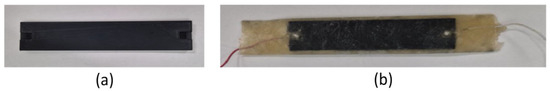
Figure 2.
Sensor assembly (a) and the sensor embedded in a GFRP-Mat composite (b).
To evaluate the sensor’s response within the composite structure, bending tests were performed under five different loading forces (20, 40, 60, 80, and 100 N). Each test cycle lasted 25 min and consisted of three stages:
Stage 1: 5 min without applied load (baseline);
Stage 2: 5 min under applied load (loading);
Stage 3: 15 min after unloading (recovery).
The corresponding results are presented in Figure 3, showing a significant variation in the recorded resistance, thereby confirming the sensor’s functionality.
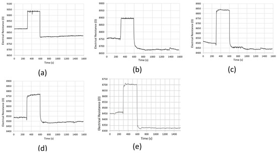
Figure 3.
Sensor response under bending load of: (a) 20 N, (b) 40 N, (c) 60 N, (d) 80 N and (e) 100 Ν.
As a general remark, the recorded resistance change (ΔR) tended to increase with applied bending force, although not strictly monotonically (e.g., 40 N force resulted to a slightly smaller ΔR than 20 N). This non-monotonic behavior observed is attributed to the conductive CNT/PLA sensing layer. In more detail, bending strain results in the construction of new conductive pathways (percolation pathways) while simultaneously causing the destruction of existing ones; this competition between the construction and destruction of the conductive routes leads to a non-monotonic behavior and is often observed for various types of CNT/polymer systems [11].
Furthermore, upon load removal, hysteresis was observed in all cases, resulting in a lower resistance value compared to the initial unloaded state. This behavior has been observed before [12] and may be attributed to minor permanent deformations induced during testing to the host composite (GFRP-Mat) or to the rearrangement of the conductive pathways within the polymer matrix—caused by bending of the assembly—as has been described previously.
As illustrated in Figure 3, the sensor’s resistance increases sharply upon bending and remains approximately constant during load application. Upon load removal, it decreases abruptly to a level slightly lower than the initial value, due to the aforementioned hysteresis.
Multiple load–unload cycles under certain bending loads were conducted on the same specimens as a preliminary investigation of device’s repeatability. The ΔR/R response remained stable. A baseline drift was observed after each unloading stage which is consistent with the hysteresis noted for CNT/polymer systems. Nevertheless, at every load application the sensor exhibited a clear and reproducible increase in resistance.
Overall, the specific results demonstrate the sensor’s consistent and reliable response to bending loads. The bending deformation at the midpoint of the sensor unit, where the load was applied, together with the deduced flexural strain and the recorded resistance values for the three testing stages, are presented in Table 2.
Table 2.
Strain and resistance of the sensor upon bending.
The sensor’s resistance variations under different loading conditions are presented in Figure 4. These variations clearly demonstrate the device’s potential to function as a strain sensor or strain detector responding consistently to the applied bending loads.
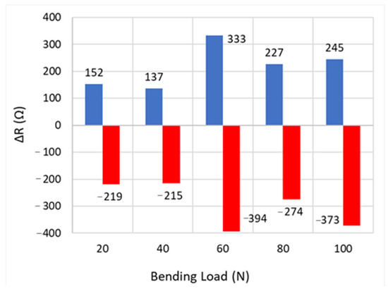
Figure 4.
Sensor’s resistance variation under different bending loads. Blue bars correspond to the applied strain, while red bars correspond to the removed strain, illustrating the sensor’s response and hysteresis behavior.
4. Conclusions
In this study, the concept of a 3D-printed strain sensor capable of generating a resistance signal in response to bending loads was successfully demonstrated. The results show that fabrication of such a device using the FDM method is feasible, and the sensor functions reliably when embedded in GFRP composites, highlighting its potential for structural health monitoring and failure prediction. The sensor assembly can be integrated directly into structural components and interfaced with electronic circuits via standard soldering of the contact pads, facilitating practical application. The sensor exhibits a consistent response under bending loads ranging from 0 to 100 N, and although hysteresis occurs during unloading, it maintains reliable sensitivity to bending deformations.
Overall, this work confirms that additive manufacturing can be employed to produce cost-effective, integrated, functional piezoresistive strain sensors tailored for composite structures, providing an option for customizable, in situ monitoring of structural performance with potential applications in marine and aerospace engineering. Future work includes exploring optimization of sensor geometry, conductive material content, and embedding strategies to further enhance sensitivity, minimize hysteresis, and extend sensor’s application to more complex structural systems.
Author Contributions
Conceptualization, D.N.P. and I.I.; methodology, D.N.P. and I.I.; validation, I.I., S.P. and N.M.N.; formal analysis, S.P., I.I. and N.M.N.; investigation, N.M.N.; writing—original draft preparation, D.N.P. and I.I.; writing—review and editing, D.N.P. and S.P.; visualization, S.P.; supervision, D.N.P. All authors have read and agreed to the published version of the manuscript.
Funding
This research received no external funding.
Institutional Review Board Statement
Not applicable.
Informed Consent Statement
Not applicable.
Data Availability Statement
The original contributions presented in this study are included in the article. Further inquiries can be directed to the corresponding author.
Acknowledgments
This work was presented at the 8th International Conference of Engineering Against Failure, Kalamata, Greece, 22–25 June 2025, and the registration fees were totally covered by the University of West Attica.
Conflicts of Interest
The authors declare no conflicts of interest.
References
- Xu, Y.; Wu, X.; Guo, X.; Kong, B.; Zhang, M.; Qian, X.; Mi, S.; Sun, W. The Boom in 3D-Printed Sensor Technology. Sensors 2017, 17, 1166. [Google Scholar] [CrossRef] [PubMed]
- Goh, G.L.; Zhang, H.; Chong, T.H.; Yeong, W.Y. 3D printing of multilayered and multimaterial electronics: A review. Adv. Electron. Mater. 2021, 7, 2100445. [Google Scholar] [CrossRef]
- Ni, Y.; Ji, R.; Long, K.; Bu, T.; Chen, K.; Zhuang, S. A review of 3D-printed sensors. Appl. Spectrosc. Rev. 2017, 52, 623–652. [Google Scholar] [CrossRef]
- Apostolakis, A.; Barmpakos, D.; Pilatis, A.; Patsis, G.; Pagonis, D.N.; Belessi, A.; Kaltsas, G. Resistivity study of inkjet-printed structures and electrical interfacing on flexible substrates. Micro Nano Eng. 2021, 15, 100129. [Google Scholar] [CrossRef]
- Fekiri, C.; Kim, H.C.; Lee, I.H. 3D-Printable Carbon Nanotubes-Based Composite for Flexible Piezoresistive Sensors. Materials 2020, 13, 5482. [Google Scholar] [CrossRef] [PubMed]
- Zheng, Y.; Huang, X.; Chen, J.; Wu, K.; Wang, J.; Zhang, X.A. Review of Conductive Carbon Materials for 3D Printing: Materials, Technologies, Properties, and Applications. Materials 2021, 14, 3911. [Google Scholar] [CrossRef]
- Liu, H.; Zhang, H.; Han, W.; Lin, H.; Li, R.; Zhu, J.; Huang, W. 3D printed flexible strain sensors: From printing to devices and signals. Adv. Mater. 2021, 33, 2004782. [Google Scholar] [CrossRef]
- Rhinoceros Modelling Tools for Designers, Version 5, SR13, 64-bit. Available online: https://www.rhino3d.com/ (accessed on 1 September 2025).
- ASTM D790; Standard Test Methods for Flexural Properties of Unreinforced and Reinforced Plastics and Electrical Insulating Materials. ASTM International: West Conshohocken, PA, USA, 1990.
- Kanoun, O.; Bouhamed, A.; Ramalingame, R.; Bautista-Quijano, J.R.; Rajendran, D.; Al-Hamry, A. Review on Conductive Polymer/CNTs Nanocomposites Based Flexible and Stretchable Strain and Pressure Sensors. Sensors 2021, 21, 341. [Google Scholar] [CrossRef]
- Christ, J.F.; Aliheidari, N.; Ameli, A.; Potschke, P. 3D printed highly elastic strain sensors of multiwalled carbon nanotube/thermoplastic polyurethane nanocomposites. Mater. Des. 2017, 131, 394. [Google Scholar] [CrossRef]
- Kouvatsos, T.; Pagonis, D.N.; Iakovidis, I.; Kaltsas, G. Towards a 3D Printed Strain Sensor Employing Additive Manufacturing Technology for the Marine Industry. Appl. Sci. 2024, 14, 6490. [Google Scholar] [CrossRef]
Disclaimer/Publisher’s Note: The statements, opinions and data contained in all publications are solely those of the individual author(s) and contributor(s) and not of MDPI and/or the editor(s). MDPI and/or the editor(s) disclaim responsibility for any injury to people or property resulting from any ideas, methods, instructions or products referred to in the content. |
© 2025 by the authors. Licensee MDPI, Basel, Switzerland. This article is an open access article distributed under the terms and conditions of the Creative Commons Attribution (CC BY) license (https://creativecommons.org/licenses/by/4.0/).