Abstract
Development of novel and inexpensive X-ray detectors is of key importance for numerous applications, such as dosimetry in nuclear and medical facilities, diagnostics in cultural heritage, and homeland security. Solution-processed materials are being investigated as novel x-ray sensing materials, with constant improvements that are rapidly approaching commercial standards. Here, we demonstrate a detector based on PbS colloidal quantum dots (QD) fabricated in air with simple drop-casting techniques on a Si substrate with pre-patterned Au interdigitated electrodes. The device showed good linearity in the tested dose range and a maximum sensitivity value of 2370 µC Gy−1 cm−1, which is higher than typically reported values for commercial a-Se and poly-CZT detectors.
1. Introduction
Efficient detection of X-ray radiation by novel, inexpensive and easily processable materials is of great importance in many fields of application, from homeland and airport security to personal dosimetry in radiology, also encompassing safety in nuclear plants. Current commercial room-temperature direct detectors often use expensive materials such as CdZnTe (CZT) or a-Se [1]. Both materials are bulky, rigid, and fragile. a-Se shows poor performance, consequently requiring a high operating voltage. CZT is expensive and difficult to grow, though it is deemed the commercial gold standard for X-ray detectors. Solution-processable materials, such as perovskites, colloidal quantum dots, organic semiconductors, and metal–organic frameworks, are promising candidates as alternative sensing materials [2]. They are often considered to be inexpensive and easily tunable. Many detectors based on these materials have been demonstrated, with exciting improvements in sensitivity, mobility, and limit of detection. Here, we investigated the use of PbS QDs as a sensing layer on a silicon substrate with gold interdigitated electrodes. Although fabricated with a simple protocol performed in air, the devices showed excellent sensing performances even with a low voltage bias of 1 V.
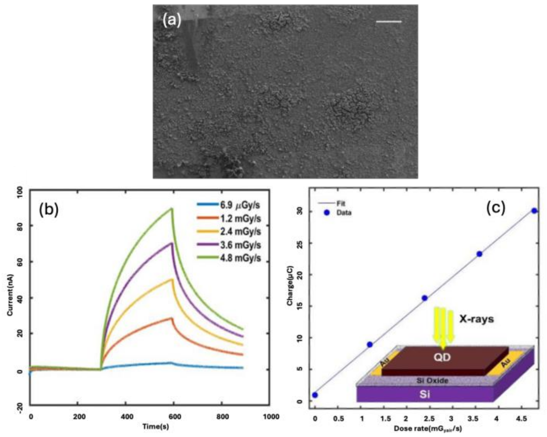
2. Materials and Methods
We performed X-ray Illumination with an Amptek mini X-2 gun and a Ag anode (sourced from Amptek Inc., Bedford, MA, USA). The dose delivered by the source was referenced with a PTW boron-doped diamond detector.
3. Discussion
The QDs colloidal solution was prepared following a modified Hines and Scholes procedure [3]. UV–Vis analysis showed band-edge absorption at ~920 nm, indicating a mean QD size of ~3 nm. The fabrication protocol of the devices was kept simple and straightforward, cyclically drop-casting the PbS QD solution onto the substrate and performing in situ ligand exchange with butylamine (BA). The final treatment for all the devices was oxidation in air at room temperature. The sensing layer was characterized by microscopy and spectrometric techniques. Scanning electron microscopy (SEM) pictures showed that the QD film was homogeneous, albeit with a limited presence of surface cracking and flaking, as can be seen in Figure 1a. Uniformity of the film was a key objective in the fabrication, as it is known that it directly affects mobility and therefore charge collection in the detector. The devices were tested under X-ray irradiation by illuminating the detectors for 300 s and measuring the photogenerated current (Figure 1b). Within the considered dose range (~7 × 10⁻⁶–5 × 10⁻³ Gyair), the devices showed good charge–dose (C-D) linearity. A typical C-D plot is reported in Figure 1c. From the slope of the C-D line, we calculated the sensitivities of the detectors, obtaining ~2.374 × 10³ μC· Gyair−1 cm−2. This excellent value is, to the best of our knowledge, higher than the best reported sensitivity for QDs X-ray direct detection [4].
Figure 1.
(a) SEM picture of the final QDs layer. The scale bar represents 100 um. (b) Photogenerated current during X-ray illumination at different dose rates. (c) Dose–charge line; the inset is a sketch of the device.
Author Contributions
Conceptualization, M.R., A.D.I., L.C. and L.T.; methodology, software, validation, investigation, M.R.; writing—original draft, M.R. and A.D.I.; writing—review and editing, M.R., A.D.I., L.T., L.C., A.F., E.M., E.C. and P.B. All authors have read and agreed to the published version of the manuscript.
Funding
This research received no external funding.
Institutional Review Board Statement
Not applicable.
Informed Consent Statement
Not applicable.
Data Availability Statement
Data is available upon reasonable request to the corresponding author.
Conflicts of Interest
The authors declare no conflicts of interest.
References
- Johns, P.M.; Nino, J.C. Room temperature semiconductor detectors for nuclear security. J. Appl. Phys. 2019, 126, 040902. [Google Scholar] [CrossRef]
- Basiricò, L.; Ciavatti, A.; Fraboni, B. Solution-Grown Organic and Perovskite X-ray Detectors: A New Paradigm for the Direct Detection of Ionizing Radiation. Adv. Mater. Technol. 2021, 6, 2000475. [Google Scholar] [CrossRef]
- Hines, M.A.; Scholes, G.D. Colloidal PbS nanocrystals with size-tunable near- infrared emission: Observation of post-synthesis self-narrowing of the particle size distribution. Adv. Mater. 2003, 15, 1844–1849. [Google Scholar] [CrossRef]
- Liu, J.; Shabbir, B.; Wang, C.; Wan, T.; Ou, Q.; Yu, P.; Tadich, A.; Jiao, X.; Chu, D.; Qi, D.; et al. Flexible, printable soft-X-ray detectors based on all-inorganic perovskite quantum dots. Adv. Mater. 2019, 31, 1901644. [Google Scholar] [CrossRef] [PubMed]
Disclaimer/Publisher’s Note: The statements, opinions and data contained in all publications are solely those of the individual author(s) and contributor(s) and not of MDPI and/or the editor(s). MDPI and/or the editor(s) disclaim responsibility for any injury to people or property resulting from any ideas, methods, instructions or products referred to in the content. |
© 2024 by the authors. Licensee MDPI, Basel, Switzerland. This article is an open access article distributed under the terms and conditions of the Creative Commons Attribution (CC BY) license (https://creativecommons.org/licenses/by/4.0/).