Article

A New Paradigm in Split Manufacturing: Lock the FEOL, Unlock at the BEOL †

1
Department of Electrical and Computer Engineering, New York University (NYU), Brooklyn, NY 11201, USA
2
Division of Engineering, New York University Abu Dhabi (NYU AD), Abu Dhabi 129188, United Arab Emirates
*
Author to whom correspondence should be addressed.
This paper is an extended version of our paper published in Proceedings of the Design Automation and Test in Europe (DATE), “A New Paradigm in Split Manufacturing: Lock the FEOL, Unlock at the BEOL”, Florence, Italy, 25–29 March 2019; pp. 414–419.
Cryptography 2022, 6(2), 22; https://doi.org/10.3390/cryptography6020022
Submission received: 15 March 2022 / Revised: 20 April 2022 / Accepted: 28 April 2022 / Published: 5 May 2022

Abstract

:
Split manufacturing was introduced as a countermeasure against hardware-level security threats such as IP piracy, overbuilding, and insertion of hardware Trojans. However, the security promise of split manufacturing has been challenged by various attacks which exploit the well-known working principles of design tools to infer the missing back-end-of-line (BEOL) interconnects. In this work, we define the security of split manufacturing formally and provide the associated proof, and we advocate accordingly for a novel, formally secure paradigm. Inspired by the notion of logic locking, we protect the front-end-of-line (FEOL) layout by embedding secret keys which are implemented through the BEOL in such a way that they become indecipherable to foundry-based attacks. At the same time, our technique is competitive with prior art in terms of layout overhead, especially for large-scale designs (ITC’99 benchmarks). Furthermore, another concern for split manufacturing is its practicality (despite successful prototyping). Therefore, we promote an alternative implementation strategy, based on package-level routing, which enables formally secure IP protection without splitting at all, and thus, without the need for a dedicated BEOL facility. We refer to this as “poor man’s split manufacturing” and we study the practicality of this approach by means of physical-design exploration.

1. Introduction

Outsourced fabrication has become the de facto standard for the semiconductor industry. However, the corresponding sharing of valuable intellectual property (IP) with all the involved, potentially untrusted parties has raised several security concerns, such as IP piracy and counterfeiting [1,2] or insertion of hardware Trojans [3]. Without countermeasures applied, these threats are becoming an increasing concern for military and/or commercial organizations. Besides massive financial losses [4], there is also potential impact on national security; it is estimated that 15% of all the spare and replacement semiconductors bought by the Pentagon are counterfeit [5].

1.1. Split Manufacturing and Its Threat Model

To address the above concerns directly at the hardware level, the Intelligence Advanced Research Projects Activity (IARPA) agency advocated split manufacturing [6,7]. The asymmetry between metal layers (Table 1) facilitates splitting of the design into two parts (Figure 1): the front-end-of-line (FEOL), which contains the active device layer and lower metal layers (usually ≤ M3), and the back-end-of-line (BEOL), which contains the higher metal layers (usually ≥ M4). The fabrication of the FEOL requires access to an advanced facility, and thus, this part is outsourced to a high-end but potentially untrusted foundry. The BEOL is subsequently grown on top of the FEOL at a low-end but trusted foundry. Several studies [6,7,8,9] have successfully demonstrated split manufacturing for complex designs and also for relatively modern process nodes such as 28 nm. Still, concerns about the practicality, yield management, and cost efficiency of split manufacturing remain within the community and industry.
The classical threat model for split manufacturing is shown in Figure 2. As the attacker resides in the FEOL foundry, the functionality of the design is hidden from him/her in the form of missing BEOL connections. Besides, the attacker cannot access a working chip copy. This is because (1) the chip is yet to be manufactured, and (2) even if another version of the chip has been manufactured previously, the end-user (e.g., a government entity), is considered trusted and will not hand out the chip. However, the attacker has access to the FEOL and full knowledge of the computer-aided chip design (CAD) tools, the technology library, etc.

1.2. Proximity Attacks and Prior Work on Countermeasures

The promise of split manufacturing has been called into question by a class of attacks known as proximity attacks. Even though the physical layout can be split during manufacturing, regular CAD tools still work on the whole layout holistically, to apply various optimization techniques. This fact, in conjunction with the deterministic nature of commercial CAD tools, is shown to leave hints in the FEOL layout part which can be exploited by an attacker to infer the missing connections. In particular, to-be-connected cells are typically placed close to each other in the FEOL, mainly to minimize delay and power. This hint of physical proximity of cells was first exploited by Rajendran et al. [10].
Consequently, several studies sought to protect split manufacturing against proximity attacks. Rajendran et al. proposed swapping of block pins to induce 50% Hamming distance (HD) between the outputs of the original netlist and that reconstructed by an attacker [10]. This defense is limited to hierarchical designs, whereas the majority of industrial designs are flattened. Moreover, the defense was shown to be weak, as ∼87% of the missing connections were inferred by the authors’ attack itself [10]. Among other considerations, Jagasivamani et al. advocated for splitting at M1 [11]. While doing so induces the maximal number of missing BEOL connections for an attacker, it also offsets the commercial benefit of outsourced fabrication. This is because the BEOL facility has to support the same fine wiring pitch of the FEOL device layer. Sengupta et al. presented placement-centric defenses to purposefully re-arrange cells far apart [12]. Although this scheme allows for strong resilience against proximity attacks, it incurs notable overheads, especially for larger designs. Further, a routing-centric defense against targeted insertion of hardware Trojans was proposed by Imeson et al., though this also comes with excessive layout overheads [13]. Magana et al. proposed inserting routing blockages in the FEOL to “trick” the router to move more nets to the BEOL [14], whereas Patnaik et al. proposed controlled lifting of selected nets to the BEOL [15,16].

1.3. Motivation and Contributions

Almost all prior work seeking to protect against proximity attacks rely on some heuristics, which can be broadly understood as perturbing the placement and/or perturbing the routing. Such schemes have two general pitfalls: (1) without any formal security guarantees, the resilience of the schemes can only be evaluated empirically, by running currently available attacks; and (2) heuristically perturbing the FEOL layout “on top” of regular design optimization tends to induce large overhead. Therefore, there is a clear need for formally secure schemes to advance split manufacturing.
To the best of our knowledge, this work represents the first formally secure scheme for split manufacturing concerning the classical threat model. (Imeson et al. [13] were the first to offer a formal notion for split manufacturing in 2013. However, their work considers a different threat model: the attacker already holds the full netlist and aims for targeted Trojan insertion. In our work, we consider the classical threat model, where the objective for the attacker is to infer the netlist given only the FEOL). We follow Kerckhoff’s principle, i.e., our approach remains secure even if all the implementation details are available except the key. We propose and follow a new paradigm for split manufacturing—lock the FEOL, unlock at the BEOL—where the resilience of the FEOL is formally underpinned with a logic locking scheme and its secret key. To this end, we lock the FEOL regularly, using a locking technique of the designer’s choice, whereas the key required for unlocking is provided through hard-wired signal assignments in the split-away BEOL. Again, we leverage the notion of logic locking only to present a formally secure technique for split manufacturing, but we do not follow the threat model of logic locking.
Our paradigm can be applied even without the need for splitting at all, namely by delegating the step of unlock at the BEOL toward package-level routing. This alternative implementation, which we refer to as “poor man’s split manufacturing”, represents an important advancement for state-of-the-art in IP protection by itself, as it eliminates common concerns about the practicality of split manufacturing. In fact, “poor man’s split manufacturing” boils down to regular chip manufacturing, just with additional I/O pins and bumps being utilized for handling of key-nets. We release our framework and benchmarks publicly [17].
The contributions of this paper are as follows:
  • A new paradigm for split manufacturing is proposed: lock the FEOL, unlock at the BEOL. The essence is to adapt the notion of logic locking to secure the layout and to explicitly route the nets holding the key through the BEOL (or even the package level).
  • We define the security promise of split manufacturing and establish our paradigm with related proof.
  • Based on this formal security analysis, we implement our paradigm without leaking any hints to foundry-based attackers, hindering any kind of proximity attacks. To that end, a CAD framework is developed for end-to-end implementation and evaluation of our scheme. The framework is based on commercial-grade tools and serves to (1) lock the FEOL by embedding key-gates into it, (2) implement the related key-bits using fixed-value signals and route the related key-nets through the BEOL (or even the package level), (3) control the layout cost, and (4) provide the split layouts for meaningful security evaluation. We release our framework and benchmarks publicly [17].
  • Extensive experiments on ITC’99 and ISCAS benchmarks are carried out to demonstrate our scheme in terms of security and overhead. For an empirical security analysis, we leverage the state-of-the-art proximity attack in [18]. Besides, we further consider an “ideal proximity attack”, providing the most powerful analysis setup, which still cannot break our scheme. Further, the overhead for our scheme is marginal.
  • We propose an alternative implementation which we call, in simple terms, “poor man’s split manufacturing”. This approach only requires a trusted packaging facility or even only board-level support, instead of a fully fledged and trusted back-end foundry. As it does not involve any splitting of the layout at all, the process for IP protection is streamlined in a less complicated and more practical way than traditional split manufacturing. We contrast “poor man’s split manufacturing” for regular IP protection versus our locking-inspired scheme, showing that ours is more practical.

2. Concept

2.1. Background and Threat Model

Our work is inspired by the notion of logic locking [19,20]. Figure 3 shows a simple example for logic locking: a so-called key-gate K0 (XOR) is inserted after the output of the regular gate G3, and unless the correct key-bit (‘0’ in this case) is applied, the functional behavior of the circuit would be erroneous. Likewise, we protect a layout by inserting a sufficient number of key-gates, which are driven by a secret key that is realized through the BEOL/package level (Figure 4 and Figure 5). We do not require dedicated locking schemes; any scheme can be applied, including the seminal work on random insertion of key-gates [19].
Nevertheless, in our work, there are significant differences to the notion of locking. Our threat model (Figure 2) is the classical one for split manufacturing, where only the foundry is untrusted. In contrast, locking seeks to protect against untrusted end-users and untrusted foundries.
This implies two consequences, as follows.
  • For locking, the notion of an untrusted end-user forces the designer to store the key in a tamper-proof memory (TPM). Such TPMs remain an active area of research with their practicality and security still limited [21,22,23]. Further, these TPMs are fed to the circuit via flip/flops (FFs) that add complexity to the overall circuit design, as follows. First, these components can significantly increase the area footprint of a circuit; e.g., for [24], a single FF and the TPM part for a single bit incur 9 μ m 2 and 1.46 μ m 2 area, respectively, using the 65 nm GlobalFoundries LPe technology; for the baseline design, this would translate to up to 25% of the total area for the whole key. Second, the secure testability of these FFs poses a significant challenge for the designer [25,26,27]. In contrast, in our case where the threat model excludes possible attacks from end-users, the key-bits are implemented through so-called TIE cells (i.e., dedicated cells providing constant logic 0/1 signals) and the related key-nets are securely delegated to the BEOL or the package. As our technique neither requires a TPM nor any additional circuitry for key handling and testing, it does not hamper the overall complexity of the circuit.
  • For ours, since chip fabrication is considered as currently ongoing (and, in any case, since the end-user is trusted), there is no physical chip copy available as an oracle, rendering oracle-guided attacks inapplicable.
Conforming with our oracle-less setup, we do not consider any invasive attacks on fabricated chip which would be conducted at run-time either by foundry adversaries or end-users, such as optical probing [28,29]. While orthogonal to our threat model, we like to note that there are package-level and other countermeasures to thwart such invasive attacks [30]. Furthermore, we acknowledge that foundry adversaries have leverage for other attacks, such as mask manipulation, e.g., to tamper or disable the locking circuitry [28]. This threat vector is a powerful and generic one; it affects all security schemes, not only ours. However, reverse engineering and verification flows, e.g., [31], may serve to detect such malicious hardware modifications, and there are also schemes for runtime monitoring of circuits even in the presence of malicious modifications, e.g., [32,33], which may be tailored to detect tampering of the locking circuitry. While such measures would require additional efforts, they are relevant—again, not only for our notion of security, but for any scheme. Finally, these attacks vectors are orthogonal to the main theme of our work; related countermeasures can be applied on top of our scheme. Again, our threat model is consistent with prior art on split manufacturing, including the seminal proximity attack [10].

2.2. Physical Embedding of the Key at the BEOL

For our paradigm of securing split manufacturing through locking, the key is not stored in a TPM, but provided by fixed-value signals. (Again, our use of locking only serves to protect layouts against foundry-based adversaries, not against end-users.) More specifically, we connect key-gates with TIE cells, which can provide the key-bits ‘1’ and ‘0’, respectively, via TIEHI and TIELO instances. However, simply connecting TIE cells with key-gates does not guarantee security by itself; a naive physical design might reveal hints for proximity attacks (Figure 4a). Consequently, these signals have to be routed through the BEOL in such a way that the key remains indecipherable to FEOL-based adversaries. Thus, we advocate the following strategies.

2.2.1. Randomized Placement of TIE Cells

To defeat any proximity attack, it is critical that the placement of TIE cells does not reveal any connectivity hints. Thus, we propose to randomize the placements of TIE cells (Figure 4b). We can reasonably expect that doing so has little impact on layout cost. This is because TIE cells are very small in comparison to regular cells, allowing them to be rearranged relatively freely without significant perturbations required for other cells. Furthermore, since TIE cells are not actual drivers, moving them randomly away from their sinks (the key-gates) neither induces larger loads, nor requires upsizing, nor undermines the efficacy of any locking scheme of choice.

2.2.2. Lifting of Key-Nets

Given that proximity attacks can also leverage the FEOL-level routing, placement randomization alone is not sufficient; we also have to protect the routing as follows. We denote the nets connecting TIE cells to key-gates, providing the key-bits to the latter, as key-nets. It is easy to see that in case a key-net is routed in full within the FEOL, the related key-bit can be readily discerned by the attacker (Figure 4a,b). Thus, we advocate a systematic and careful lifting of all key-nets to the BEOL (Figure 4c). Once the design is split, the lifted key-nets shall form broken connections without any proximity hints remaining for an FEOL-centric attacker (Figure 4d). Such lifting of key-nets does not undermine the efficacy of any locking scheme of choice.

2.3. Physical Embedding of the Key at the Package Level: “Poor Man’s Split Manufacturing”

We would like to emphasize again that the security of our scheme stems from successfully hiding the key assignment from FEOL-centric adversaries. Thus, instead of carefully routing key-nets through the BEOL and separating these metal layers from the FEOL manufacturing procedure by means of split manufacturing, an alternative implementation strategy is to simply connect key-gates to regular I/O ports, without any re-routing or splitting. Note that I/O ports are handled independently of regular placement and routing of standard cells, hence they do not reveal any information by themselves to foundry-based adversaries. I/O ports are physically connected to bumps which, in our scheme, are in turn connected to fixed-value signals only later on, either using package routing at a trusted packaging facility or during regular board-level routing at a trusted assembly facility (Figure 5). Therefore, no splitting into FEOL and BEOL is required at all for this approach.
The strategy outlined above holds two distinct advantages over traditional split manufacturing. First, there are benefits related to capital cost. Traditional split manufacturing requires access to a trusted BEOL facility which, although more low-end than actual device fabrication, can still cost upward of USD ∼1 B. For example, in the context of the 45 nm technology node, depending on the split layer (M3 or M6), a facility such as GlobalFoundries’ 110 nm Fab 6 (representative of M3) and 350 nm Fab 2 (representative of M6) required investments of USD 1.4 B USD and USD 1.3 B, respectively [34]. Further, IARPA’s Trusted Integrated Chips (TIC) program [6] demonstrated split manufacturing using IBM’s fab (now GlobalFoundries’ Fab 9) with facilities that cost USD 1.5 B. This economic burden clearly limits the applicability of split manufacturing. However, a chip-assembly facility costs only a fraction of wafer fabs, sometimes as low as 50 M USD [35,36]. Thus, the above outlined strategy has greater economic viability, hence our terminology of “poor man’s split manufacturing”. The second advantage is that this strategy streamlines all the related processes, eliminating associated complexities such as splitting the manufacturing flow, re-organizing the supply chain logistics, protection and shipping of incomplete wafers, taking up manufacturing of additional BEOL layers, and the alignment for those BEOL layers. In fact, this strategy boils down to regular chip manufacturing.
We explain in Section 4 in more detail how we handle both strategies (embedding the key at the BEOL versus embedding the key at the package level) using commercial CAD tools. Besides, it is important to note that our locking-inspired scheme requires only one I/O port/bump per key-bit, and the handling of key-nets through the package/board level will not impact the chip’s performance. Thus, in contrast to prior work, our scheme is particularly suitable for “poor man’s split manufacturing”. We discuss these aspects in more detail in a case study in Section 5.5.

3. Formal Security Analysis

We formally define the problem of split manufacturing and highlight the underlying notion of security. Without loss of generality, we assume n inputs, m outputs, and k key-bits.
As for “poor man’s split manufacturing”, while this strategy does not infer any actual, physical splitting, it can still be understood as “splitting” just after the top-most BEOL layer, rendering the whole layout the FEOL part and only the connections for I/O nets subject to such “splitting”. As reasoned below, given that our security notion depends only on key-nets, not regular nets, and further given that key-nets for “poor man’s split manufacturing” are delegated to I/O nets, this strategy is formally secure as well.
Definition 1.
Let a combinational circuit be denoted as C, where C implements a Boolean function F : I O ; I { 0 , 1 } n and O { 0 , 1 } m , i.e., C ( x , i ) = F ( i ) i I , where x are the combinational elements of C. (We formalize here for only combinational circuits, but the notion can be readily extended for sequential designs). Thus, a split manufacturing scheme S can be defined as follows:
1. 
A split procedure is a function G : C ( x ) { C ( x 1 , x 2 ) , λ ( x 2 ) } , where x 1 denotes the elements whose connections are complete, whereas x 2 denotes the elements which are left unconnected. λ ( x 2 ) contains the connectivity information for x 2 .
2. 
C ( x 1 , x 2 ) is outsourced to the FEOL facility, whereas λ ( x 2 ) is completed at a trusted BEOL/packaging facility, i.e., it remains the secret.
3. 
A circuit is compiled by completing λ ( x 2 ) connections on C ( x 1 , x 2 ) which can be viewed as a function H : { C ( x 1 , x 2 ) , λ ( x 2 ) } C h ( x ) such that C h ( x , i ) = C ( x , i ) , i I .
Hence, the security relies on successfully hiding λ ( x 2 ) from the untrusted foundry. The success of the attacker can be measured by the difficulty of his/her ability to recover λ ( x 2 ) from C ( x 1 , x 2 ) . Let us assume an attacker A Δ , following an attack strategy Δ , tries to recover λ ( x 2 ) . We say the attack is successful if and only if λ ( x 2 ) λ ( x 2 ) , such that
C h ( x , i ) = C ( x , i ) , i I , w h e r e C h ( x ) = H ( C ( x 1 , x 2 ) , λ ( x 2 ) ) a n d λ ( x 2 ) A Δ ( C ( x 1 , x 2 ) )
Definition 2.
A split manufacturing scheme S is considered to be secure if, for any probabilistic polynomial time (PPT) attacker, the probability of finding λ ( x 2 ) λ ( x 2 ) is not greater than ϵ ( γ ) , i.e.,
P r [ λ ( x 2 ) λ ( x 2 ) ] ϵ ( γ )
where a function ϵ is negligible iff c N , γ 0 N such that γ γ 0 , ϵ ( γ ) < γ c , with γ being the security parameter.
The following theorem establishes the security of our proposed scheme against proximity attacks.
Theorem 1.
Our proposed scheme is secure against a PPT attacker following the strategy of [18], denoted as Ψ, (Any proximity attack relies on some hints in the layout. We believe that our security-centric design and physical implementation of the key renders such hints void. In any case, once further hints would become prominent for future attacks, our scheme can be extended accordingly), i.e.,
P r [ λ ( x 2 ) λ ( x 2 ) ] ϵ ( γ ) ; λ ( x 2 ) A Ψ ( C ( x 1 , x 2 ) ) .
Proof outline. The success of any proximity attack hinges on FEOL-level hints that can be exploited to infer the missing connections. Specifically, the seminal attack in [18] discusses (1) physical proximity between connected cells, (2) routing paths in the FEOL, (3) load constraints for drivers, (4) unlikeliness of combinational loops, and (5) timing constraints. It is important to understand that none of these hints apply to our scheme due to the following:
  • Physical proximity between TIE cells and key-gates, for regular split manufacturing, is dissolved by randomizing the placement of TIE cells. Again, such re-arrangement of TIE cells does not undermine the efficacy of any locking scheme of choice, given that TIE cells only provide the logical key-bit values, and do not carry any meaning beyond that. For connections between I/O ports and key-gates, for “poor man’s split manufacturing”, the notion of physical proximity is inapplicable. This is because the placement of I/O ports is independent of any gate placement, avoiding any correlation between proximity and connectivity.
  • FEOL-level routing of key-nets for regular split manufacturing is controlled by lifting key-nets directly at the cells’ pins as a whole to the BEOL, using stacked vias both at the TIE cell’s output pin and at the key-gate’s input pin (Figure 4; also see Section 4). This way, any directional wiring which might otherwise leave hints is avoided to begin with. For FEOL-level routing to I/O ports, for “poor man’s split manufacturing”, the related directionality does not reveal any information by itself. Again, this is due to I/O port placement being independent of gate placement.
  • Load capacitance constraints are neither applicable to TIE cells nor to I/O ports; both are no actual drivers.
  • Combinational loops are absent from any key-net path by default, since TIE cells as well as I/O ports are not driven by any other gates themselves. Thus, avoiding loops for open nets cannot help an attacker rule out incorrect connections of key-nets.
  • Timing constraints do not apply to TIE cells or I/O ports, as they define only static paths for key-nets.
In the following proof, we leverage the assumptions from the proof outline above. As a consequence, an attacker is forced to brute-force the key, which becomes exponentially hard in the number of key-bits used to lock the design.
Proof. 
The probability of guessing the correct key-bit for each key-gate is P k b = 1 2 . Let us assume the probability of finding the correct connection for all other, regular nets is P o . Thus, the probability of successfully recovering all connections is
P r [ λ ( x 2 ) λ ( x 2 ) ] = P o × P k b P k b = i = 1 k 1 2 + ϵ ϵ ( k )
where k is the number of key-bits. Note that as the security of our scheme depends only on the key-nets, not the regular nets, we can ignore P o . Additionally, note that, for regular split manufacturing, correctly inferring all split nets does pose a significant challenge (see also Section 5.1). Nevertheless, following Kerckhoff’s principle, we base our formalism only on the key-nets, because for “poor man’s split manufacturing” all regular nets are readily available to the attacker. Thus, our scheme is secure—for both manifestations, regular split manufacturing as well as “poor man’s split manufacturing”—assuming a sufficiently large number of key-bits [37].    □
While one might want also argue for key-extraction attacks against logic locking, in particular, SAT-based attacks such as [38], recall the different threat model and the absence of an oracle for our scheme that makes such attacks inapplicable. Other potential attacks are discussed in Section 5.4.

4. Physical Design Framework

We implement our scheme using commercial-grade tools. Figure 6 illustrates the flow; details are given next. We release our framework and benchmarks publicly [17].

4.1. Synthesis for Logic Locking

First, we emphasize the fact that our scheme is generic and agnostic to the underlying locking technique. For a meaningful case study, but without loss of generality, we utilize the seminal random logic locking technique [19] in this work. Further, we use 80 key-bits, which is deemed secure according to modern security standards [37].
The key steps we follow for introducing locking during synthesis are to (1) introduce key-gates into the circuit, (2) drive the key-gates with TIE cells, and (3) synthesize the circuit keeping the key-gates and TIE cells as is. Some details are discussed next. Since key-nets driven by TIE cells are interpreted as hard-coded input for the key-gates, we must avoid re-structuring them during synthesis. We do so by utilizing the specific tool commands set_dont_touch and set_dont_touch_network on the TIE cells and key-nets, respectively. Further, we ensure that the key is drawn uniformly at random from { 0 , 1 } k for k representing the length of the key. Doing so translates to an even distribution of TIEHI and TIELO cells in the layout; thus, an attacker cannot derive any hints from the distribution of TIE cells.

4.2. Layout Generation for Regular Split Manufacturing

As previously indicated, rendering the process of layout generation secure for our scheme applied in the context of regular split manufacturing consists essentially of two steps: (1) randomizing the placement of TIE cells, and (2) lifting the key-nets to the BEOL.
First, we detach the TIE cells from the key-gates to avoid inducing any layout-level hints on those key-gates. Second, we randomly re-arrange and fix the placement of TIE cells (the latter again by utilizing the tool command set_dont_touch on the TIE cells). Next, detailed placement and routing of the locked design is completed. Afterward, the key-gates are re-attached, and the design is re-routed using ECO routing to lift the key-nets to the BEOL. For this, we declare routing constraints such that stacked vias are used directly at the output pins of all TIE cells and the input pins of all key-gates. These constraints ensure that key-nets are lifted as whole to the BEOL; such constraints can be easily declared for different split layers. For ECO routing, we enforce routing of key-nets as new nets, while other regular nets are automatically re-routed as need be.
In Figure 7, we illustrate the outlined handling of TIE cells and key-nets as an example for the benchmark b14_C, with M6 as split layer of choice. The random placement of TIE cells can be inferred from the criss-cross-like routing of key-nets in Figure 7(top). In Figure 7(bottom), we highlight the routing of one selected key-net. It can be seen that the whole key-net is routed exclusively in M7 and M8, enabled by stacked vias (not visible) used directly on top of the cell pins. Thus, we demonstrated that all key-nets are routed through the BEOL only. We further confirmed this from the wirelength reports.

4.3. Layout Generation for “Poor Man’s Split Manufacturing”

This alternative stage for layout generation also starts with the synthesized and locked netlist, as described in Section 4.1. Thereafter, this stage serves to lift all the key-nets to the top-most metal layer and to connect the lifted nets with bumps.
First, the design is placed and optimized in a regular flow. Next, based on the number of key-nets to be lifted, new I/O ports are created at the top-level module. These new I/O ports are to be assigned to I/O bumps (during the bump_assign step). To this end, we devise a temporary standard cell, or TS cell for short, which enables us to lift any net of choice and connect it directly to the I/O bumps. The TS cell comprises two pins: (1) A which is to be connected to a standard cell, and (2) PAD which is to be connected to an I/O bump. The pin PAD is configured as CLASS BUMP, to enable it to be connected with an I/O bump. Note that we allow such direct connections to I/O bumps through a custom cell only, since we ensure that the related signals are routed at the package level and do not constitute regular, external I/O connections. (Regular I/O connections would have to be handled through dedicated pad cells.) Both the pins are defined in the layer BA; along with layer BB and the RDL, this top-most layer is used for routing with bumps. Note that the accordingly revised LEF and timing information for this TS cell (as copied from BUF_X2) are loaded during the init_design step.
For each key-net, one TS cell is inserted at a random location, with pin A connected to the sink (key-gate), whereas pin PAD is connected to the dedicated, newly created I/O port and routed toward the I/O bump using the specific tool command fcroute. Finally, after routing all key-net segments, the TS cells are removed again, and the design is finalized. Note that the key-bit assignments are eventually realized by connecting the VDD/VSS signals to the corresponding I/O bumps; this step is not illustrated here in detail as it subject to the trusted packaging facility, not us as acting as designers.

5. Experimental Results

All experiments were carried out on an 128-core Intel Xeon processor running at 2.2 GHz with 794 GB of RAM. All the codes are compiled using GNU C compiler 8.1.0 on Cent OS 6.9 (Final). We use Synopsys Design Compiler (DC), Cadence Innovus, and Cadence SiP, along with the 45 nm Nangate OpenCell library [39] for regular split manufacturing as well as the GlobalFoundries 55LPe technoloy, related standard cell libraries from ARM, and I/O libraries from Aragio for “poor man’s split manufacturing”.

5.1. Security Analysis

Besides the formal analysis in Section 3, we establish the validity of our work with an empirical study using the seminal proximity attack described in [18].
In the context of our scheme, we note that the attack [18] has the following limitation: it may falsely connect a key-gate to a regular driver instead of a TIE cell. Since we assume that an attacker has full understanding of our scheme and can differentiate between key-gates and regular gates in the FEOL, it is critical to address this issue for an accurate analysis. Thus, for any key-gate being falsely connected to a regular driver, we post-process the netlist to randomly re-connect this key-gate to a TIE cell. However, key-gates already connected by the attack to a TIE cell are kept as is.
Correct connection rate (CCR). The CCR is the ratio of correctly inferred connections to that of the total number of broken connections. The lower the CCR, the better the protection or, conversely, the higher the CCR, the better the attack. Since the security of our scheme depends on the key-nets, we report CCR for regular nets and key-nets separately. Further, for key-nets, we differentiate between physical and logical CCR as follows: (1) physical CCR considers whether key-nets are physically correct, i.e., if the original routing from the particular TIE cells to the particular key-gates is deciphered, and (2) logical CCR considers whether key-nets are logically correct, i.e., if key-gates are connected to any TIE cell of correct logical value.
Note that logical CCR is an important metric for us—as an attacker has full knowledge of the key-gates, she is only interested in deciphering the correct logical values for these key-gates, viz., TIEHI or TIELO. From a security-enforcing designer’s perspective, the logical CCR should ideally be ∼50%, which would imply that an attacker does no better than a random guess; recall Section 3.
In Table 2, we report the regular/physical CCR for two different setups, viz., lifting of key-nets to M5 and M7, while splitting at M4 and M6, respectively. For regular nets, as expected, CCR improves for higher split layers. For key-nets, however, physical CCR remains ∼0% for all cases. This confirms our claim of a physically secure key design.
Additionally, we report the logical CCR for key-nets in Table 2. Recall that we post-process falsely connected key-gates for the attack [18], implying an advantage and fair assumption for the attack as is. Still, we note that the logical CCR, is on average, ∼49%, i.e., the attack performs no better than a random guess. Further, any slight deviation from 50% cannot by readily leveraged by an attacker; she cannot know which particular key-bits are correct/incorrect without using an oracle, which is not available, to begin with. Thus, she is left with possible choices in an exponential range for the number of key-bits.
Hamming distance (HD) and output error rate (OER). The HD and OER both serve to quantify the difference in functional behavior between the original netlist and the one recovered by the attacker when stimulated with varying input patters. From the defender’s perspective, the ideal HD and OER are 50% and 100%, respectively.
From Table 3, we see that the proximity attack is unable to recover the full functionality of the original netlist. While HD is ∼40% for the layouts split at M4, we note that HD drops for the layouts split at M6. This is because when splitting at a higher layer, an attacker can readily obtain a larger part of the design from the FEOL, namely in the form of regular nets. Nonetheless, OER is 100% and logical CCR for key-nets is ∼49% even for higher layers, establishing the security of our technique. Independently, the designer may also increase the number of key-bits to also raise the HD for higher split layers.
Further, we establish the security of our scheme under the strongest possible threat model. Namely, we conduct an experiment where we assume that all regular nets have been correctly inferred; only key-nets remain to be deciphered. Now, as established in Section 3 and empirically verified above, an attacker cannot do better than randomly guessing the key-nets. Therefore, we apply 1 M runs for randomly guessing the key-nets. For these experiments, the OER remains at 100% across all benchmarks, establishing the security of our schemes even in the presence of such an ideal attack.
Comparison with prior work. Recall that most prior art employs some heuristic measures for advancing IP protection in the context of split manufacturing (Section 1.2), with their implementation efforts and resulting resilience being further subject to security-unaware physical-design tools. In contrast, our scheme offers formal security guarantees concerning the classical threat model for the first time, and our implementation efforts are rendered secure by construction.
Nevertheless, for a meaningful study, we assess our work against prior work, and the results are presented in Table 4. As preset by those prior studies, here we leverage the ISCAS benchmarks and evaluate CCR, HD, OER, and percentage of netlist recovery (PNR). Note that PNR measures the structural similarity between the protected netlist and the one obtained by the attacker [15]; the lower the PNR, the better the protection. Note that CCR for ours refers to the physical CCR of the key-nets. It is evident from Table 4 that ours is competitive or even superior to the prior art.

5.2. Layout Analysis

Figure 8 illustrates the layout costs across all considered ITC’99 benchmarks. The respective baselines are the regular, unprotected layouts. We would like to emphasize that all regular and locked layouts have only few (<20), if any, outstanding DRC issues. To this end, we reduce the utilization rates as needed. Hence, area is reported in terms of die outline.
The Prelift configuration serves as a crucial reference point as it quantifies the baseline cost incurred by locking—it covers the locked layouts as generated using a regular physical design flow, but with TIE cells and key-nets marked as “don’t touch” (i.e., Figure 4a). Here, we observe acceptable area overhead of ∼4% on average. This is attributed to the addition of key-gates and TIE cells in the design (Section 4). We note a ∼6% increase for power on average, whereas performance remains similar, with ∼0.3% savings on average. This can be attributed to TIE cells not being actual drivers, and key-nets only forming static paths; both are barely impacting the performance of the circuit. Next, we discuss the costs for the final layouts when compared with the unprotected layouts. Notably, area cost remains unchanged, i.e., ∼4% for both splitting at M4 and M6. Here, power is increased by ∼4.6% and ∼5.7% when splitting at M4 and M6, respectively. For performance, cost is limited to −0.5% and −0.7% for M4 and M6, respectively.
In short, our design process imposes acceptable cost along with formal security guarantees.
Comparison with prior work. Few works report on layout costs incurred by their schemes. Recently, [15,16] report layout cost, but for ISCAS benchmarks which contain only few hundreds of cells. On average, these schemes incur 10.7%/15.0%/9.2% [15] and 11.5%/10.0%/0.0% [16] cost for power/performance/area, respectively.
The cost for our scheme is competitive with these prior works in terms of power and area, and we can even obtain performance savings which these prior works cannot, all the while securing the more practically relevant, large-scale ITC’99 benchmarks. For the ISCAS benchmarks, our approach may incur a higher cost. For example, for c7552, we observe 17.6%/4.3%/20.9% for power/performance/area costs for splitting at M4. This is because, due to the small circuit size, the key-gates and TIE cells form a considerable part of the design—the cost can only be amortized for larger benchmarks, as we have shown for the ITC’99 benchmarks. We might also argue that protecting the IP in overly small designs such as the ISCAS benchmarks is not meaningful.

5.3. Reducing the Number of TIE Cells

For the benefit of improving area utilization and routability, we note that the number of TIE cells could be reduced down to two—a pair of one TIELO and one TIEHI cell—all without undermining the security promises of our scheme in principle. This is because an attacker does not have any knowledge about the distribution of the key-bits other than that it is random and uniform. Next, we re-run all our experiments while using only a single pair of TIE cells.
Correct connection rate (CCR).Table 5 reports the CCR for three different setups, viz., for lifting of key-nets to M5, M7, and M9 while splitting at M4, M6, and M8, respectively.
The physical CCR for key-nets increases somewhat for higher split layers. This indicates that, for this special case of using only a single pair of TIE cells, the physical layout may still contain some FEOL-level hint(s) which can leak information about the key-net connections. While the logical CCR follows a similar trend, the deviation from the ideal remains marginal. In any case, recall that an attacker cannot benefit from any deviation without having an oracle made available to her (which is out of the threat model).
Hamming distance (HD) and output error rate (OER). In Table 6, we report HD for the functionality of the recovered versus original netlists as on average 35.1%, 16.0%, and 6.2% for split layer M4, M6, and M8, respectively. Although the HD drops considerably toward higher layers, the OER remains 100% across layers. This confirms that the proximity attack is still ineffective in recovering the full functionality of the original netlist.
Layout analysis.Figure 9 illustrates the layout costs across all considered ITC’99 benchmarks when using a single pair of TIE cells. The area overhead remains within ∼3% across the split layers, which is slightly less than what we observed before, i.e., ∼4% when employing more TIE cells. More importantly, previously we had failed to generate DRC/LVS-clean layouts for split layer M8 without incurring prohibitive area overheads, whereas here we can. The power and performance overheads also remain unchanged across layers, i.e., ∼6% and ∼0%, respectively.
Summary. Using only a single pair of TIE cells does not compromise the foundational security of our scheme, albeit some marginal improvements for the attack have been observed. Further, this configuration is well-suited for splitting at higher layers and managing related layout costs.

5.4. Discussions

Runtime. Our experiments on large-scale ITC’99 benchmarks (30 K+ gates) take a few minutes. The most time-consuming step is re-routing. This is due to the fact that lifting the key-nets can initially introduce several DRC errors into the layout, which take some time to resolve.
Impact of key-size. It is clear from Table 3 and Table 6 that the higher the split layer, the lower the HD and the better the functional behavior of the recovered netlist matches the original netlist. This is because, while splitting at higher layers, an attacker can readily obtain a larger part of the design from the FEOL through regular nets.
Recall that we lock all designs using 80-bit keys, which is deemed sufficient for today’s computational standard [37]. However, a designer is free to insert more key-gates, e.g., alternatively guided by fractions of the total number of gates in the design. To demonstrate the impact on HD and OER, we conduct such experiments on the b14_C circuit, where we insert key-gates in steps of 5%, 10%, 15%, 20%, and 25% of all gates, respectively. The results are reported in Table 7. As expected, the HD increases with a larger key-size. Nevertheless, we would like to emphasize again that even for 80 key-bits, the OER remains 100% across all benchmarks, establishing the security of our scheme.
Impact of split layer. Another important observation from our experiments is that the logical CCR remains close to the ideal value (50%) and comparable across different split layers, specifically for the first configuration of using multiple TIE cells (recall Table 2). This indicates that the security of our scheme is independent of the split layer, i.e., key-nets can potentially be split at any layer without compromising the security of our scheme. To this end, we conduct another experimentation for the circuit c432, where we evaluate the logical CCR for splitting at M1–M8. The related CCR results are reported in Table 8. We observe that, indeed, the security remains unaffected across different split layers, without any clear trend for CCR deviations.
This insight also serves as a motivational reminder for “poor man’s split manufacturing”, where we show next that the key-nets can in fact be routed through the package-routing facility without compromising security.

5.5. “Poor Man’s Split Manufacturing”

As introduced in Section 2.3, another interesting strategy to advance the practicality of split manufacturing is to delegate nets to be protected to the package or even the board level. Doing so avoids the need for any physical splitting procedure to begin with, thereby enabling better viability for IP protection at manufacturing time. However, for any prior protection schemes, this approach is limited in the scale of realizable IP protection: obfuscating any regular net this way requires two I/O ports/bumps, one to route the net out (to establish the “hidden parts” of the net via package/board-level routing) and one to route the net back into the chip. Given that bumps, along with their minimum pitch requirements, occupy relatively large areas, their presence in great numbers could easily enforce to enlarge die outlines, thereby directly impacting silicon cost. Moreover, such detouring of regular nets through bumps and package/board-level routing can have a significant impact on the performance of the design.
For our locking-inspired scheme, these limitations are considerably relaxed: we require only one bump per key-net, and having these key-nets implemented in the package/board level will not impact the chip’s performance.
Next, we provide a case study to quantify the benefits of our locking-inspired scheme over regular IP protection in the context of “poor man’s split manufacturing”. The study is centered on a previously taped-out design of an ARM Cortex-M0 core with various custom modules; this serves well for a practical and relevant evaluation. We leverage the GlobalFoundries 55LPe technology, standard cell libraries from ARM, and I/O libraries from Aragio for this study.
Overview. We implement two different design cases for this study: (a) regular IP protection versus (b) our locking-inspired scheme. For (a), we randomly choose 80 single-fanout nets of the ARM core to be protected. These nets are lifted and then re-routed through the package level, thereby obfuscating them from fab-based adversaries. For (b), we use 80 key-bits for locking and implement the resulting key-nets through the package level. For both cases, the required physical-design steps have been explained in detail in Section 4. Note that, although the steps have been introduced with particular focus on key-nets in that Section 4, we can handle any other net in a similar manner as well.
Both design cases are illustrated in Figure 10. For a fair comparison, the following settings apply for both cases: chip dimensions are 3280 μm × 3280 μm, and timing and utilization constraints are set to 15 ns and 0.6, respectively.
Bump assignment. For Figure 10(top), lifting of regular nets to the package level, there are 160 signal bumps incurred to protect the 80 single-fan out nets, whereas for Figure 10(bottom), our locking-inspired scheme, there are only 80 signal bumps incurred for the 80 key-nets. As a result, there are (a) 44 versus (b) 95 bumps remaining for the power/ground (P/G) network. While we do not evaluate the power-delivery network here, it is understood that allowing for more P/G bumps is beneficial in any case. Additionally, as we would complete routing of the lifted nets at the package level (applies to both regular nets as well as key-nets), recall that our flow allows us to wire up bumps directly with their corresponding standard cells, bypassing the pads which are used otherwise for regular I/O connections.
Design metrics. In Table 9, we report on the key metrics for both design cases. For fair comparison, layout costs for both cases are put in a common context for a regular, unprotected baseline implementation of the same design.
As we strive for a fair comparison, we ensured the same chip dimensions, utilization rates, and timing constraints for both cases. Thus, neither case incurs additional silicon cost; this is because the number of gates remains comparable, whereas the dominating factor for die outlines are bumps. As expected, the impact on timing for lifting of regular nets is significant; this is because of the relatively lengthy detours toward the package level and back. For key-nets, as they are not part of timing paths, there is no impact at all on performance. The impact on power incurred by lifting of regular nets is higher as well, namely twice that for lifting of key-nets; this is because lifting of regular nets requires additional buffering, whereas key-nets are static and do not require such buffering. As indicated, we can afford for more P/G bumps (more than double) when lifting key-nets instead of regular nets and, at the same time, we can even further relax the bump spacing/pitch requirement by 12.5%.
Comparison to traditional split manufacturing. We understand that “poor man’s split manufacturing” might appear as a weaker method when compared to traditional split manufacturing, in the sense that the number of nets hidden from a fab-based attacker are potentially limited by the considerable layout costs induced while delegating lifted nets through additional I/O bumps. However, note that hiding of regular nets has no security implications on our manifestation of “poor man’s split manufacturing”. In fact, its security stems only from successfully hiding the secret key-bits, as elaborated in Theorem 1 in Section 3. Given this, “poor man’s split manufacturing” can deliver sufficient and provable security by lifting only a handful of key-nets as compared to traditional split manufacturing schemes, which rely on a sufficiently large number of regular nets being either cut as is, lifted and cut, or otherwise perturbed, but in general rendered difficult to recover for an attacker. For ours, the use of locking ensures that particular parts of the design are truly secured with only a limited number of key-nets lifted; “poor man’s split manufacturing” is not relying on heuristics for layout/routing perturbation as other works on split manufacturing.
Summary. We have demonstrated the practicality and lower layout costs for our scheme versus regular IP protection through a comparative study on an ARM Cortex-M0 design. Our scheme incurs only half the number of additional signal bumps for the same scale of nets being protected/locked. Thereafter, several beneficial options arise for our scheme, which the designer is free to trade-off as needed: (a) for the same die outline and commercial cost, increase the number of key-nets/key-bits, thereby increasing the level of security; (b) reduce the die outline and thus commercial cost; or (c) increase the number of P/G bumps to strengthen the power-delivery network.

6. Conclusions

For the first time, we present a formally secure scheme for split manufacturing concerning the classical threat model. Our paradigm is to lock the FEOL by embedding a secret key; this is in fundamental contrast with current defense schemes, which all rely on heuristic techniques (e.g., layout-level perturbations). For our paradigm, the secret key required for unlocking is to be implemented through the BEOL. Using commercial-grade tools, we develop a design flow to embed the key such that it becomes indecipherable to an FEOL-centric proximity attack. Any proximity attack must rely on FEOL-level hints, and such hints are inherently avoided for the secret key by our core techniques of randomizing TIE cells and lifting the key-nets in full. We release our framework and benchmarks publicly [17].
We present results on large-scale ITC’99 benchmarks that further validate our formal claims. Two notable findings are as follows. First, we show that our scheme is secure against a state-of-the-art proximity attack, which cannot perform better than randomly guessing the key bits. Second, the resilience of key-nets is independent of the split layer.
For that latter finding, we propose an alternative approach called “poor man’s split manufacturing”, where a trusted packaging facility replaces the trusted BEOL fab. As the security of our approach stems from hiding the bit assignments for the key-nets, these nets can also be connected to the I/O ports and bumps of a chip and, in turn, tied to fixed logic at the (trusted) package routing/board level. We demonstrate the practicality of this approach through a case-study on the ARM Cortex-M0 microcontroller.

Author Contributions

Conceptualization, A.S. and O.S.; data curation, A.S., M.N. and M.A.; formal analysis, A.S. and J.K.; funding acquisition, O.S.; investigation, A.S., M.N. and M.A.; methodology, A.S., M.N., M.A. and J.K.; project administration, A.S. and J.K.; software, A.S., M.N. and M.A.; supervision, J.K. and O.S.; validation, A.S.; visualization, A.S.; writing—original draft, A.S., J.K. and O.S.; writing—review and editing, A.S., J.K. and O.S. All authors have read and agreed to the published version of the manuscript.

Funding

This work is partially sponsored by the New York University/New York University Abu Dhabi (NYU/NYUAD) Center for Cyber Security (CCS). The work of A. Sengupta was supported in part by the Global Ph.D. Fellowship at NYU/NYU AD.

Institutional Review Board Statement

Not applicable.

Informed Consent Statement

Not applicable.

Data Availability Statement

Not applicable.

Conflicts of Interest

The authors declare no conflict of interest.

References

  1. Follet, J. CRN Cisco Channel at Center of FBI Raid on Counterfeit Gear. 2018. Available online: www.crn.com/networking/207602683 (accessed on 12 March 2022).
  2. Xilinx V. Flextronics: Insight to a Gray Market. 2013. Available online: http://blog.optimumdesign.com/xilinx-v-flextronics-insight-to-a-gray-market (accessed on 12 March 2022).
  3. The Big Hack: How China Used a Tiny Chip to Infiltrate U.S. Companies. 2018. Available online: https://www.bloomberg.com/news/features/2018-10-04/the-big-hack-how-china-used-a-tiny-chip-to-infiltrate-america-s-top-companies (accessed on 12 March 2022).
  4. Innovation Is at Risk as Semiconductor Equipment and Materials Industry Loses up to $4 Billion Annually Due to IP Infringement. 2008. Available online: http://www.marketwired.com/press-release/innovation-is-risk-as-semiconductor-equipment-materials-industry-loses-up-4-billion-850034.htm (accessed on 12 March 2022).
  5. Detecting and Removing Counterfeit Semiconductors in the U.S. Supply Chain. 2013. Available online: https://www.semiconductors.org/clientuploads/directory/DocumentSIA/Anti%20Counterfeiting%20Task%20Force/ACTF%20Whitepaper%20Counterfeit%20One%20Pager%20Final.pdf (accessed on 12 March 2022).
  6. IARPA. IARPA Trusted Integrated Chips (TIC) Program. 2016. Available online: https://www.ndia.org/-/media/sites/ndia/meetings-and-events/divisions/systems-engineering/past-events/trusted-micro/2016-august/mccants-carl.ashx (accessed on 12 March 2022).
  7. Jarvis, R.; McIntyre, M. Split Manufacturing Method for Advanced Semiconductor Circuits. U.S. Patent 7,195,931, 27 March 2007. [Google Scholar]
  8. Hill, B.; Karmazin, R.; Otero, C.; Tse, J.; Manohar, R. A split-foundry asynchronous FPGA. In Proceedings of the Custom Integrated Circuits Conference, San Jose, CA, USA, 22–25 September 2013; pp. 1–4. [Google Scholar] [CrossRef] [Green Version]
  9. Vaidyanathan, K.; Das, B.P.; Sumbul, E.; Liu, R.; Pileggi, L. Building trusted ICs using split fabrication. In Proceedings of the International Symposium on Hardware-Oriented Security and Trust, Arlington, VA, USA, 6–7 May 2014; pp. 1–6. [Google Scholar]
  10. Rajendran, J.; Sinanoglu, O.; Karri, R. Is split manufacturing secure? In Proceedings of the Design, Automation & Test in Europe Conference & Exhibition (DATE), Grenoble, France, 18–22 March 2013; pp. 1259–1264. [Google Scholar] [CrossRef]
  11. Jagasivamani, M.; Gadfort, P.; Sika, M.; Bajura, M.; Fritze, M. Split-fabrication obfuscation: Metrics and techniques. In Proceedings of the IEEE International Symposium on Hardware-Oriented Security and Trust (HOST), Arlington, VA, USA, 6–7 May 2014; pp. 7–12. [Google Scholar] [CrossRef]
  12. Sengupta, A.; Patnaik, S.; Knechtel, J.; Ashraf, M.; Garg, S.; Sinanoglu, O. Rethinking split manufacturing: An information-theoretic approach with secure layout techniques. In Proceedings of the IEEE/ACM International Conference on Computer-Aided Design (ICCAD), Irvine, CA, USA, 13–16 November 2017; pp. 326–329. [Google Scholar]
  13. Imeson, F.; Emtenan, A.; Garg, S.; Tripunitara, M.V. Securing Computer Hardware Using 3D Integrated Circuit (IC) Technology and Split Manufacturing for Obfuscation. In Proceedings of the USENIX Security Symposium, Washington, DC, USA, 14–16 August 2013; pp. 495–510. [Google Scholar]
  14. Magaña, J.; Shi, D.; Davoodi, A. Are Proximity Attacks a Threat to the Security of Split Manufacturing of Integrated Circuits? In Proceedings of the International Conference on Computer-Aided Design, Austin, TX, USA, 7–10 November 2016. [Google Scholar]
  15. Patnaik, S.; Knechtel, J.; Ashraf, M.; Sinanoglu, O. Concerted wire lifting: Enabling secure and cost-effective split manufacturing. In Proceedings of the Asia and South Pacific Design Automation Conference (ASP-DAC), Jeju, Korea, 22–25 January 2018; pp. 251–258. [Google Scholar]
  16. Patnaik, S.; Ashraf, M.; Knechtel, J.; Sinanoglu, O. Raise Your Game for Split Manufacturing: Restoring the True Functionality Through BEOL. In Proceedings of the ACM/ESDA/IEEE Design Automation Conference (DAC), San Francisco, CA, USA, 24–28 June 2018; pp. 140:1–140:6. [Google Scholar]
  17. Sengupta, A.; Nabeel, M.; Ashraf, M. Poor Man’s Split Manufacturing. GitHub. 2022. Available online: https://github.com/DfX-NYUAD/Poor-Man-s-Split-Manufacturing (accessed on 12 March 2022).
  18. Wang, Y.; Chen, P.; Hu, J.; Li, G.; Rajendran, J. The Cat and Mouse in Split Manufacturing. Trans. VLSI Syst. 2018, 26, 805–817. [Google Scholar] [CrossRef]
  19. Roy, J.A.; Koushanfar, F.; Markov, I.L. Ending Piracy of Integrated Circuits. Computer 2010, 43, 30–38. [Google Scholar] [CrossRef]
  20. Sengupta, A.; Nabeel, M.; Limaye, N.; Ashraf, M.; Sinanoglu, O. Truly Stripping Functionality for Logic Locking: A Fault-based Perspective. Trans. Comp.-Aided Des. Integ. Circ. Syst. 2020, 39, 4439–4452. [Google Scholar] [CrossRef]
  21. Tuyls, P.; Schrijen, G.J.; Škorić, B.; van Geloven, J.; Verhaegh, N.; Wolters, R. Read-Proof Hardware from Protective Coatings. In Proceedings of the Cryptographic Hardware and Embedded Systems, Yokohama, Japan, 10–13 October 2006; pp. 369–383. [Google Scholar]
  22. Anceau, S.; Bleuet, P.; Clédière, J.; Maingault, L.; Rainard, J.l.; Tucoulou, R. Nanofocused X-Ray Beam to Reprogram Secure Circuits. In Proceedings of the Cryptographic Hardware and Embedded Systems, Taipei, Taiwan, 25–28 September 2017; pp. 175–188. [Google Scholar]
  23. Courbon, F.; Skorobogatov, S.; Woods, C. Direct charge measurement in Floating Gate transistors of Flash EEPROM using Scanning Electron Microscopy. In Proceedings of the International Symposium for Testing and Failure Analysis, Fort Worth, TX, USA, 6–10 November 2016; pp. 1–9. [Google Scholar]
  24. Sengupta, A.; Nabeel, M.; Yasin, M.; Sinanoglu, O. ATPG-based cost-effective, secure logic locking. In Proceedings of the VLSI Test Symposium (VTS), San Francisco, CA, USA, 22–25 April 2018; pp. 1–6. [Google Scholar]
  25. Guin, U.; Zhou, Z.; Singh, A. Robust Design-for-Security Architecture for Enabling Trust in IC Manufacturing and Test. IEEE Trans. Very Large Scale Integr. Syst. 2018, 26, 818–830. [Google Scholar] [CrossRef]
  26. Limaye, N.; Sengupta, A.; Nabeel, M.; Sinanoglu, O. Is Robust Design-for-Security Robust Enough? Attack on Locked Circuits with Restricted Scan Chain Access. In Proceedings of the International Conference on Computer-Aided Design (ICCAD), Westminster, CO, USA, 4–7 November 2019; pp. 1–8. [Google Scholar]
  27. Limaye, N.; Sinanoglu, O. DynUnlock: Unlocking Scan Chains Obfuscated using Dynamic Keys. In Proceedings of the Design, Automation & Test in Europe Conference & Exhibition (DATE), Grenoble, France, 9–13 March 2020; pp. 270–273. [Google Scholar]
  28. Engels, S.; Hoffmann, M.; Paar, C. The End of Logic Locking? A Critical View on the Security of Logic Locking. Cryptology ePrint Archive, Report 2019/796. 2019. Available online: https://eprint.iacr.org/2019/796 (accessed on 12 March 2022).
  29. Rahman, M.T.; Tajik, S.; Rahman, M.S.; Tehranipoor, M.; Asadizanjani, N. The Key is Left under the Mat: On the Inappropriate Security Assumption of Logic Locking Schemes. 2019. Available online: https://eprint.iacr.org/2019/719 (accessed on 12 March 2022).
  30. Rahman, M.T.; Rahman, M.S.; Wang, H.; Tajik, S.; Khalil, W.; Farahmandi, F.; Forte, D.; Asadizanjani, N.; Tehranipoor, M. Defense-in-Depth: A Recipe for Logic Locking to Prevail. arXiv 2019, arXiv:1907.08863. [Google Scholar] [CrossRef] [Green Version]
  31. Lippmann, B.; Unverricht, N.; Singla, A.; Ludwig, M.; Werner, M.; Egger, P.; Duebotzky, A.; Graeb, H.; Gieser, H.; Rasche, M.; et al. Verification of physical designs using an integrated reverse engineering flow for nanoscale technologies. Integration 2020, 71, 11–29. [Google Scholar] [CrossRef]
  32. Wahby, R.S.; Howald, M.; Garg, S.; Walfish, M. Verifiable ASICs. In Proceedings of the Symposium on Security and Privacy (SP), San Jose, CA, USA, 22–26 May 2016; pp. 759–778. [Google Scholar]
  33. Nabeel, M.; Ashraf, M.; Patnaik, S.; Soteriou, V.; Sinanoglu, O.; Knechtel, J. 2.5D Root of Trust: Secure System-Level Integration of Untrusted Chiplets. Trans. Comp. 2020, 69, 1611–1625. [Google Scholar] [CrossRef]
  34. List of Semiconductor Fabrication Plants. 2020. Available online: https://en.wikipedia.org/wiki/List_of_semiconductor_fabrication_plants (accessed on 12 March 2022).
  35. Brinton, J.B.; Lineback, B.J.R. Packaging Is Becoming Biggest Cost in Assembly, Passing Capital Equipment. 1999. Available online: https://www.eetimes.com/packaging-is-becoming-biggest-cost-in-assembly-passing-capital-equipment/ (accessed on 12 March 2022).
  36. Kanellos, M. Intel Plans Chip Packaging Center in China. 2003. Available online: https://www.cnet.com/news/intel-plans-chip-packaging-center-in-china/ (accessed on 12 March 2022).
  37. Smart, N. ECRYPT II Yearly Report on Algorithms and Keysizes (2011–2012). 2012. Available online: http://www.ecrypt.eu.org/ecrypt2/documents/D.SPA.20.pdf (accessed on 12 March 2022).
  38. Subramanyan, P.; Ray, S.; Malik, S. Evaluating the security of logic encryption algorithms. In Proceedings of the IEEE International Symposium on Hardware Oriented Security and Trust (HOST), Washington, DC, USA, 5–7 May 2015; pp. 137–143. [Google Scholar] [CrossRef]
  39. NanGate FreePDK45 Open Cell Library. 2011. Available online: http://www.nangate.com/?page_id=2325 (accessed on 12 March 2022).
  40. Wang, Y.; Chen, P.; Hu, J.; Rajendran, J. Routing Perturbation for Enhanced Security in Split Manufacturing. In Proceedings of the Asia and South Pacific Design Automation Conference (ASP-DAC), Chiba, Japan, 16–19 January 2017; pp. 605–610. [Google Scholar]
Figure 1. Concept of split manufacturing, with splitting realized after M3 (without loss of generality). The FEOL by itself is missing the BEOL interconnects; hence, an FEOL-centric attacker has to infer those BEOL parts to obtain the full design.
Cryptography 06 00022 g001
Figure 2. The classical threat model for split manufacturing, as also considered in this work. Red dashes mean the entity is untrusted (FEOL fab), whereas green dashes mean the entities are trusted (all others).
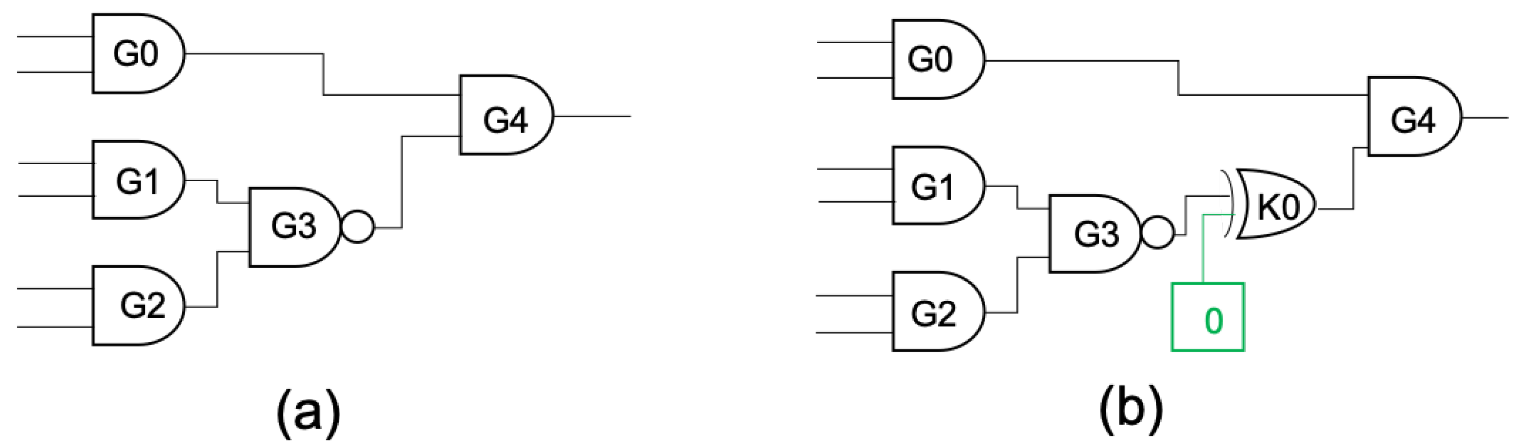
Cryptography 06 00022 g002
Figure 3. Simple example for logic locking. (a) Original circuit; (b) locked circuit with one key-gate (correct key-bit is ‘0’).
Cryptography 06 00022 g003
Figure 4. Physical design of the key for regular split manufacturing. (a) Locked layout, with key-nets connected to TIE cells, but following a regular, security-wise naive physical design. The placement of TIE cells, as well as the FEOL-level routing, can leave hints on the underlying assignment of key-bits to key-gates. (b) Locked layout of (a), with randomized placement of TIE cells. (c) Locked layout of (b), with key-nets lifted to the BEOL (i.e., above the split layer, which is M3 here). Note that lifting makes use of stacked vias to reduce FEOL-level routing and related hints to the bare minimum. (d) Locked layout of (c) after splitting. The broken key-nets are indecipherable for the FEOL-centric attacker.
Cryptography 06 00022 g004
Figure 5. Physical design of the key for “poor man’s split manufacturing”. Instead of using TIE cells and requiring the related placement and routing to avoid any hints, this strategy here simply connects key-gates to I/O ports and bumps, which do not reveal any information by themselves. The key-bits can be implemented as fixed-value signals either (a) at a trusted packaging facility or (b) at the board level.
Cryptography 06 00022 g005
Figure 6. Our physical design flow. After the synthesis stage, the flow is bifurcated into regular split manufacturing (SM) with lifting of key-nets to the BEOL versus “poor man’s split manufacturing” with lifting of key-nets to the package level. For the latter, TS cell is short for temporary cell, a custom cell we devise to enable lifting of nets to the package level.
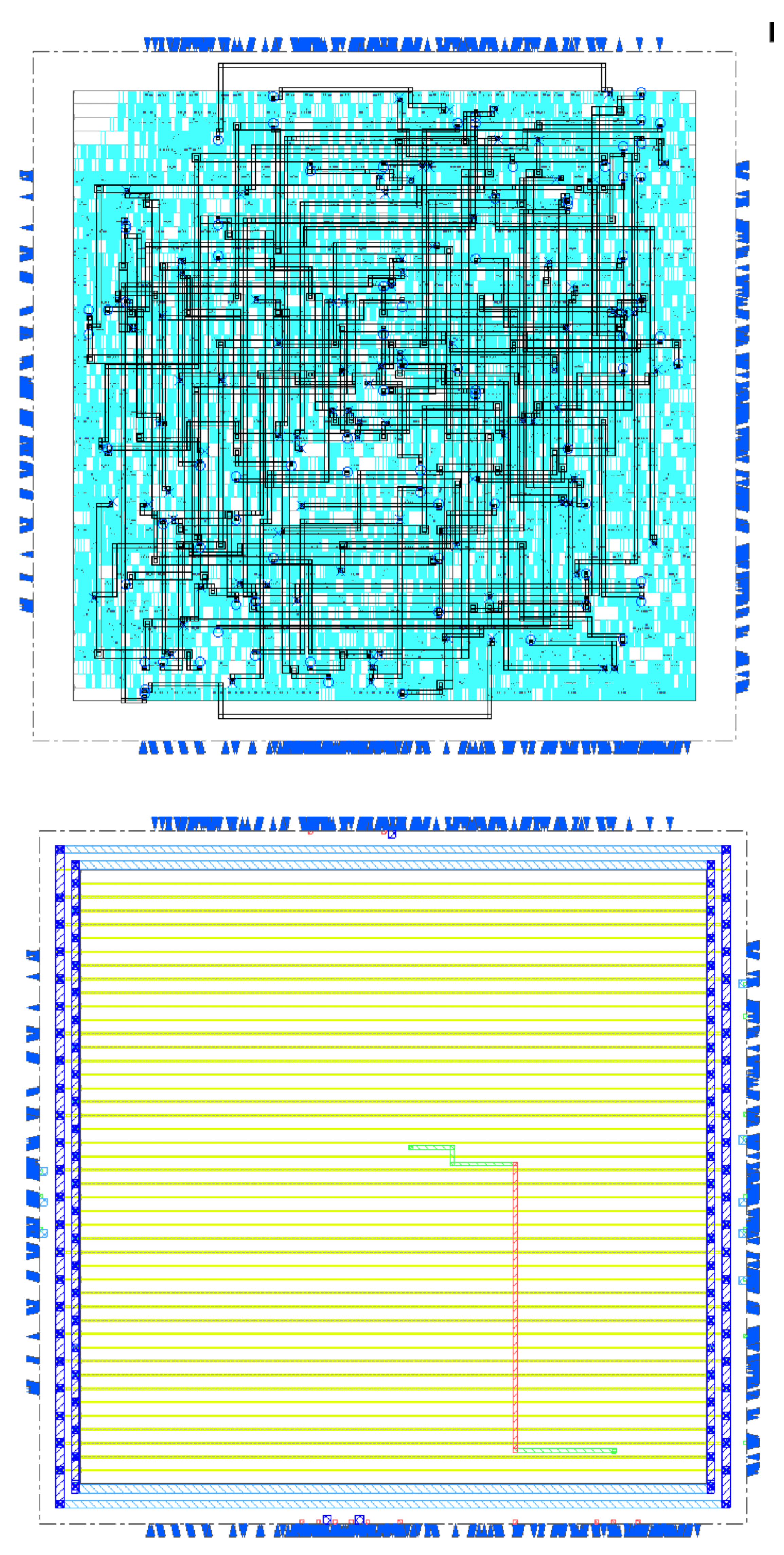
Cryptography 06 00022 g006
Figure 7. Randomized placement of TIE cells and key-nets lifted to the BEOL for benchmark b14_C, with M6 as split layer. For visibility in hard copies, colors are inverted. (top) Wiring of all key-nets, indicating that TIE cells and key-gates are decoupled. (bottom) A key-net highlighted. Routing is handled exclusively in M7 (green wire segments) and M8 (red segments).
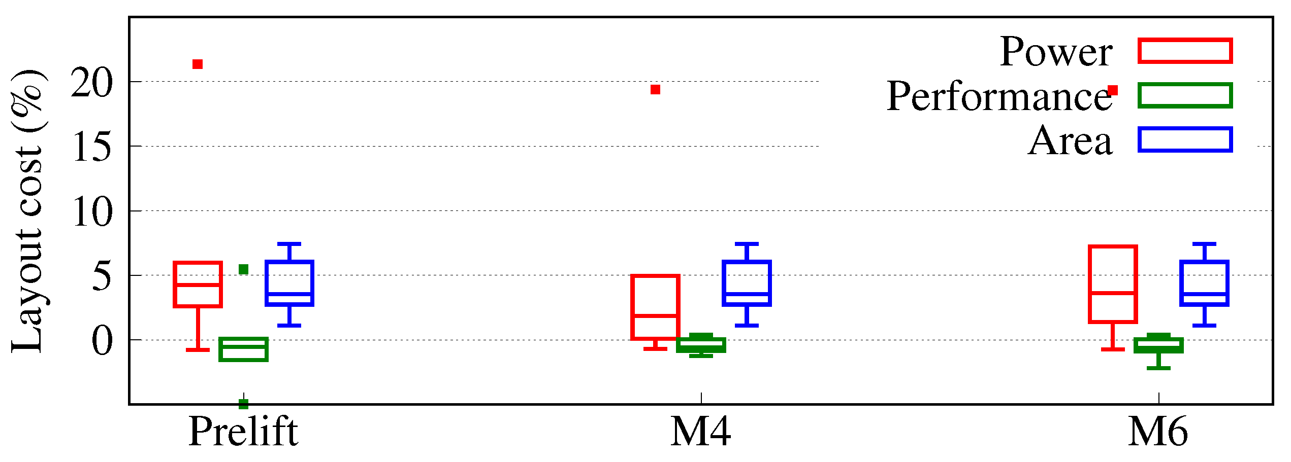
Cryptography 06 00022 g007
Figure 8. Layout costs for our scheme for various split layers. The respective baselines are the unprotected layouts. Prelift refers to locked layouts without lifting of key-nets. Each box comprises data points within the first and third quartile; the bar represents the median; the whiskers the minimum/maximum values; and outliers are marked by dots.
Cryptography 06 00022 g008
Figure 9. Layout costs for our scheme for various split layers, and when using a single pair of TIE cells. The respective baselines are the unprotected layouts. Prelift refers to locked layouts without lifting of key-nets. Each box comprises data points within the first and third quartile, the bar represents the median; the whiskers; and the minimum/maximum values, and outliers are marked by dots.
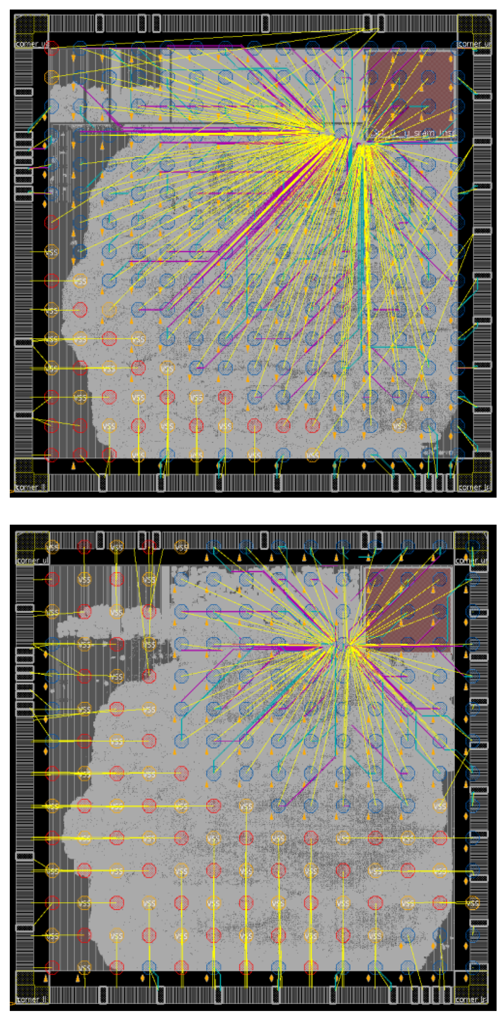
Cryptography 06 00022 g009
Figure 10. Layout and bump assignment for our case study on “poor man’s split manufacturing”, based on an ARM Cortex M0 core with various custom modules. (top) Design with lifting of 80 regular, single-fanout nets of the core. (bottom) Design with lifting of 80 key-nets, used to lock the core. Blue bumps are signal bumps and red/orange bumps are VDD/VSS bumps. Yellow flylines indicate the connectivity between bumps and the corresponding standard cells/pads. Recall that lifted nets are allowed to connect directly from cell to bump and vice versa. Most of the flylines radiate toward a region in the upper-right corner which is where the Cortex M0 core is placed.
Cryptography 06 00022 g010
Table 1. Pitches (nm) across metal layers for the Nangate 45 nm technology.
M1M2M3M4M5M6M7M8M9M10
707070140140140400400800800
Table 2. CCR (%) for ITC’99 benchmarks when split at M4 and M6. “NA” means time-out after 48 h.
Benchmark  M4M6
Key-NetsRegularKey-NetsRegular
LogicalPhysicalNetsLogicalPhysicalNets
b14501.818.548.40.925.3
b1549.6024.548.40.932
b17NANANA49.2024.5
b2047.60.917.749.91.831.0
b2147.8014.848.3031.8
b2249.4016.848.5036.3
Average48.90.518.448.80.630.2
Table 3. HD (%) and OER (%) for ITC’99 benchmarks when split at M4/M6, for 1 M simulation runs/input patterns considered. “NA” means attack time-out after 48 h.
Benchmark  M4M6
HDOERHDOER
b1434.310013.0100
b1538.510015.9100
b17NANA26.4100
b2041.110018.7100
b2142.710024.4100
b2241.910022.4100
Average39.710020.1100
Table 4. PNR, CCR, HD, and OER (all in %) for ISCAS benchmarks when split at M4. “NA” means not reported in the respective publication.
Benchmark  [40][15][16]Proposed
PNRCCRHDOERPNRCCRHDOERPNRCCRHDOERPNRCCRHDOER
c43287.578.846.199.432.3045.9100NA048.499.913.13.739.598.9
c88086.845.818.099.928.3039.9100NA043.499.916.8038.7100
c135584.977.126.610032.8046.1100NA040.199.910.23.441.4100
c190891.283.838.810029.5048.1100NA046.299.99.92.733.7100
c354086.277.036.110030.8046.4100NA047.999.98.3040.8100
c531587.774.718.110031.6035.4100NA038.399.921.71.623.8100
c755293.973.920.310026.9025.7100NA027.899.926.20.924.1100
Average88.373.329.199.930.3041.1100NA041.799.915.21.834.699.8
Table 5. CCR (%) for ITC’99 benchmarks when split at M4, M6, and M8, and when using a single pair of TIE cells. “NA” means time-out after 48 h.
BenchmarkM4M6M8
Key NetsRegular NetsKey NetsRegular NetsKey NetsRegular Nets
LogicalPhysical LogicalPhysical LogicalPhysical
b1447.91.149.544.28.823.237.525.311.7
b1546.10.923.147.61.833.845.82.723.2
b17NANANA44.88.723.645.25.236.1
b2016.9027.447.8049.243.66.638.8
b2145.51.923.947.72.845.442.79.440.5
b2246.16.548.845.56.548.843.810.828.4
Average46.52.134.546.34.837.343.110.029.8
Table 6. HD (%) and OER (%) for ITC’99 benchmarks when split at M4/M6/M8, for 1M simulation runs/input patterns considered, and when using a single pair of TIE cells. “NA” means attack time-out after 48 h.
Benchmark  M4M6M8
HDOERHDOERHDOER
b1421.91009.71007.7100
b1539.010015.31006.8100
b17NANA23.21007.2100
b2037.910018.51004.8100
b2139.710011.31004.5100
b2237.210011.91006.3100
Average35.110016.01006.2100
Table 7. Impact of key-size on HD and OER (%) for circuit b14_C when split at M6. The key-size is defined as percentage of the total number of gates in the circuit.
Key-Size (%)510152025
HD / OER (%)15.0/10024.0/10031.0/10036.5/10039.7/100
Table 8. Impact of split layer on logical CCR for the circuit c432.
Split LayerM1M2M3M4M5M6M7M8
Logical CCR49.948.649.649.948.649.049.249.2
Table 9. Case study on “poor man’s split manufacturing”. S. is short for signal (bump).
Metric/Design CaseRegular Nets LiftedKey-Nets Lifted
Timing Cost423%0%
Die-Area Cost0%0%
Power Cost3.12%1.56%
Lifted Nets8080
Bumps: Lifted S.S./Total160/18180/101
Bump: Power/Total44/22595/196
Bump Spacing200 μm225 μm
Timing Constraint15 ns15 ns
Utilization Rate0.60.6
Gates≈180 K≈180 K
Publisher’s Note: MDPI stays neutral with regard to jurisdictional claims in published maps and institutional affiliations.

