1. Introduction
Hall Effect sensors are widely used in industrial applications for a series of low power applications, including current-sensing, position detection, and contactless switching. Such magnetic sensors, integrated in regular CMOS technology, prove to be cost-effective and offer high performance [
1]. In order to guarantee Hall Effect sensors optimal behavior, high sensitivity, low offset, and low temperature drift are performance aspects that need to be achieved. Previous papers by the authors investigated the temperature effects on both sensitivity and offset [
2,
3]. The present paper is highly focused on Hall Effect sensors design, integration, and performance investigation. To achieve good results while still preserving the integration process, the sensors geometrical configuration is to be exploited [
4,
5]. As the extensive measurements performed and presented by the authors [
6] prove, there is offset variance with geometry. The project specifications, a few times better than the actual state-of-the-art in terms of offset and its drift, have been reached and various good candidates have been revealed. The present paper is structured as follows. The second section is intended to offer an overview on Hall Effect sensors basic considerations and the most important equations governing their behavior. Within this section, arguments for sensors geometry selection and design details are presented. Extensive measurements results concerning the sensors sensitivity, offset, and its temperature drift are incorporated in the third part of the present paper. The fourth section is devoted to presenting three-dimensional physical simulations used to predict the sensors’ behavior. The results and discussion are part of the fifth section of this work. Finally, the conclusions are drawn.
3. Experimental Section
3.1. Hall Effect Sensor Measurements
In order to accurately test the Hall Effect sensors, an automated measurements setup has been built [
6]. Previous papers in the literature were devoted to Hall sensors current measurements [
10].
The nine integrated Hall cells are presented in
Table 1. Part 1 of the table refers to the cross-like Hall cells, while Part 2 focuses on the square Hall cells. The table summarizes both geometrical design parameters and measurements results for the input resistance at room temperature
R0, absolute sensitivity
SA, offset drift,
etc. The design parameters include
L,
W, and
s, which stand for sensors length, width, and sensing contacts length respectively.
The information for the offset refers to the four-phases residual offset and it is an average on eleven tested samples. For offset drift measurements, a TEMPTRONICS temperature control system was used and the temperature was cycled from 0 to 90 °C.
From the measurements results, we can see that there is offset and sensitivity variance with geometry. The XL cell proved to have the best performance in terms of offset drift. There is a decrease of the borderless sensitivity compared to the other cells due to the position of contacts with respect to the borders.
Table 1.
Integrated Hall Effect devices characterization.
3.2. Offset Temperature Drift Measurement Results Using a DC Measurement Setup and Manual Phase Switching
The offset is a parasitic effect that adds to the total Hall voltage. The offset was measured in the absence of magnetic field (B = 0 T), by using a zero-Gauss chamber. The offset is defined as follows:
In order to have information on the offset of each individual phase, manual phase switching was performed. Both two-phases and four-phases residual offsets were measured.
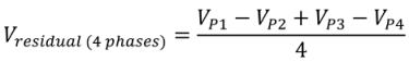
The four-phases residual offset in V is computed as follows:
where
Vp1,2,3,4 are the individual phases offsets.
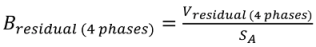
The magnetic-equivalent offset (measured in T) is defined by dividing the four-phases residual offset in V by the absolute sensitivity, as follows:
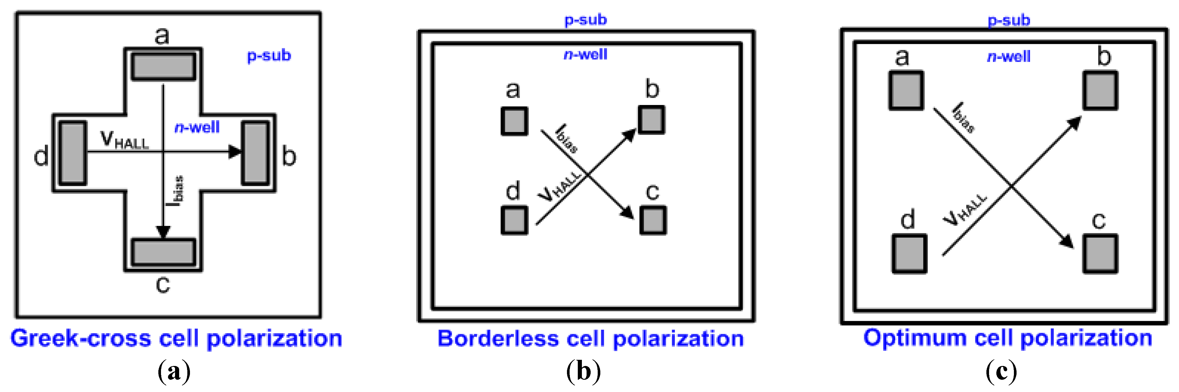
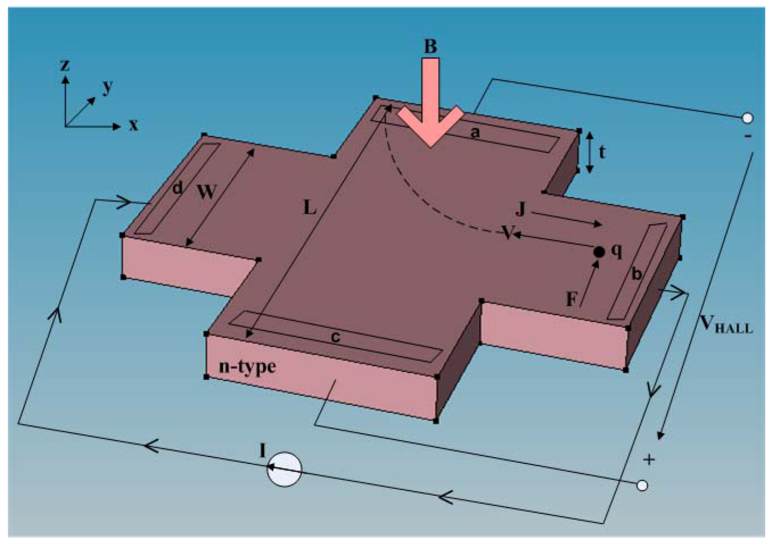
Figure 4.
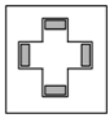
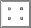
Hall cells polarization for Greek-cross cells (a), borderless cell (b) and optimum cell (c).
Figure 4.
Hall cells polarization for Greek-cross cells (a), borderless cell (b) and optimum cell (c).
In
Figure 4, the specifical Hall cells polarization is represented, for the Greek-cross cells, borderless and optimum cells respectively.
Further on,
Table 2 presents the four phases used for Hall cells polarization, including biasing and sensing contacts.
Table 2.
The corresponding polarization phases.
Table 2.
The corresponding polarization phases.
| Phases | Ibias | VHALL |
|---|
| (biasing) | (sensing) |
|---|
| Phase 1 | a to c | b to d |
| Phase 2 | d to b | a to c |
| Phase 3 | c to a | d to b |
| Phase 4 | b to d | c to a |
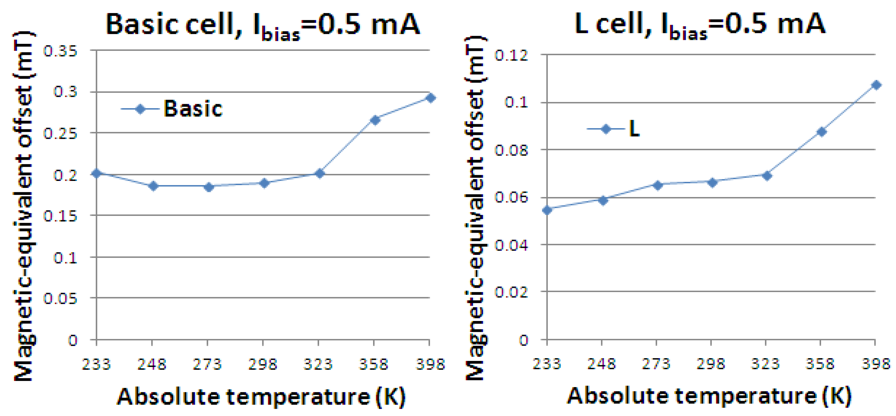
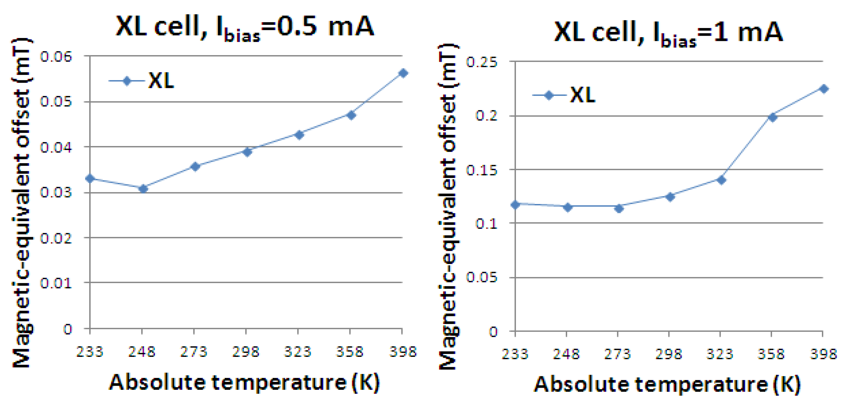
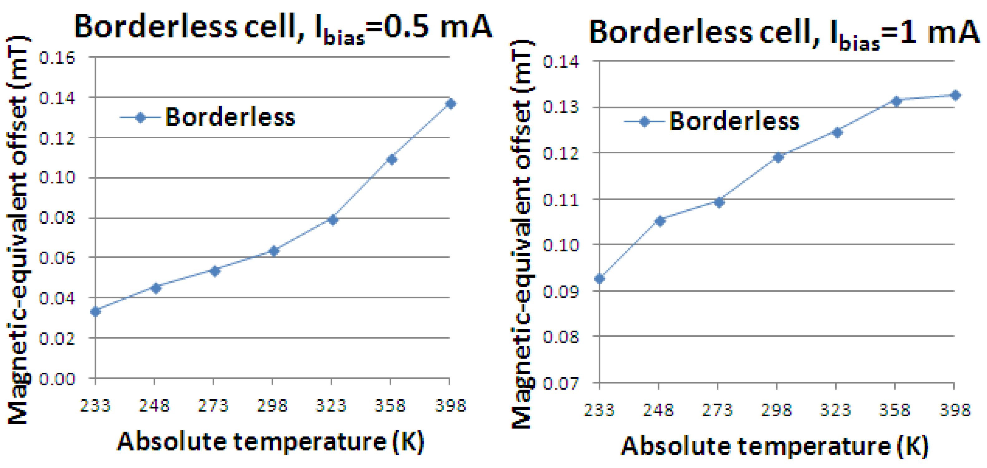
In
Figure 5,
Figure 6,
Figure 7, the magnetic equivalent residual offset
vs. absolute temperature for four different Hall Effect sensors is depicted. Two different biasing currents were taken into account,
Ibias = 0.5 mA and
Ibias = 1 mA respectively. The samples were placed into an oven and the temperature was cycled between −40 and 125 °C. We can observe the parabolic temperature dependence of the residual offset.
Figure 5.
Magnetic-equivalent offset vs. absolute temperature for the basic (left) and L (right) Hall cells, for Ibias = 0.5 mA.
Figure 5.
Magnetic-equivalent offset vs. absolute temperature for the basic (left) and L (right) Hall cells, for Ibias = 0.5 mA.
Figure 6.
Magnetic-equivalent offset vs. absolute temperature for the XL Hall cell, for Ibias = 0.5 mA (left) and Ibias = 1 mA (right).
Figure 6.
Magnetic-equivalent offset vs. absolute temperature for the XL Hall cell, for Ibias = 0.5 mA (left) and Ibias = 1 mA (right).
Figure 7.
Magnetic-equivalent offset vs. absolute temperature for the borderless Hall cell, for Ibias = 0.5 mA (left) and Ibias = 1 mA (right).
Figure 7.
Magnetic-equivalent offset vs. absolute temperature for the borderless Hall cell, for Ibias = 0.5 mA (left) and Ibias = 1 mA (right).
3.3. Room Temperature Offset Measurement Results Using an Automated AC Measurement Setup
Using an automated measurement setup presented in detail by the authors in a recent paper [
6], the proposed Hall cells have been tested and subsequently evaluated. In this sense eleven samples, each one containing 64 cells (the first eight different geometries in
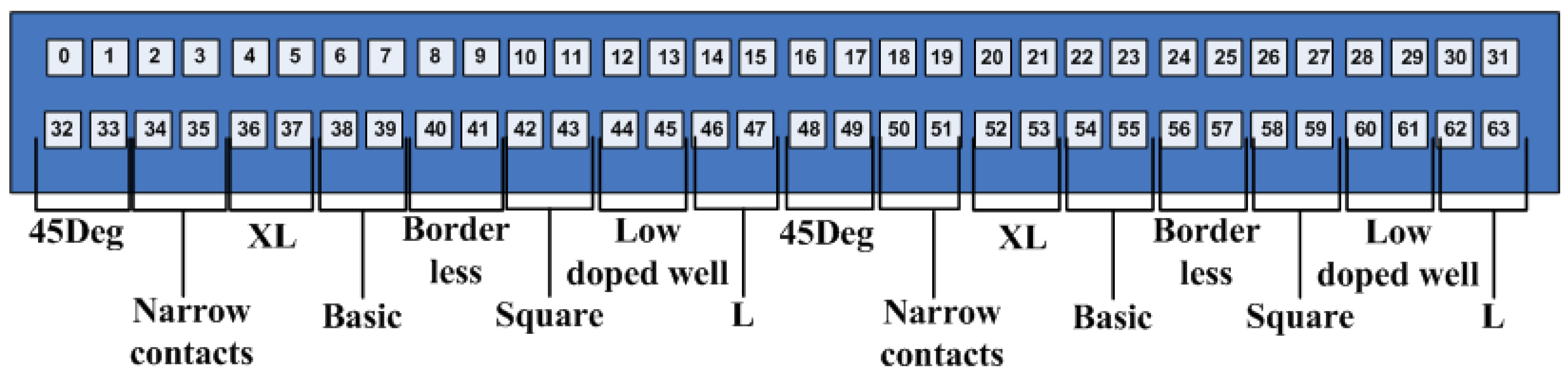
Table 1 times eight locations), were tested. The positioning of the eight cells as repetitions of eight is presented in
Figure 8. We wanted to have the same cell several times, and at different locations on the chip in order to investigate possible offset variation due to position. Therefore, the same cell was tested eight times on the same chip.
Figure 8.
Location of the eight analyzed Hall cells on a tested chip.
Figure 8.
Location of the eight analyzed Hall cells on a tested chip.
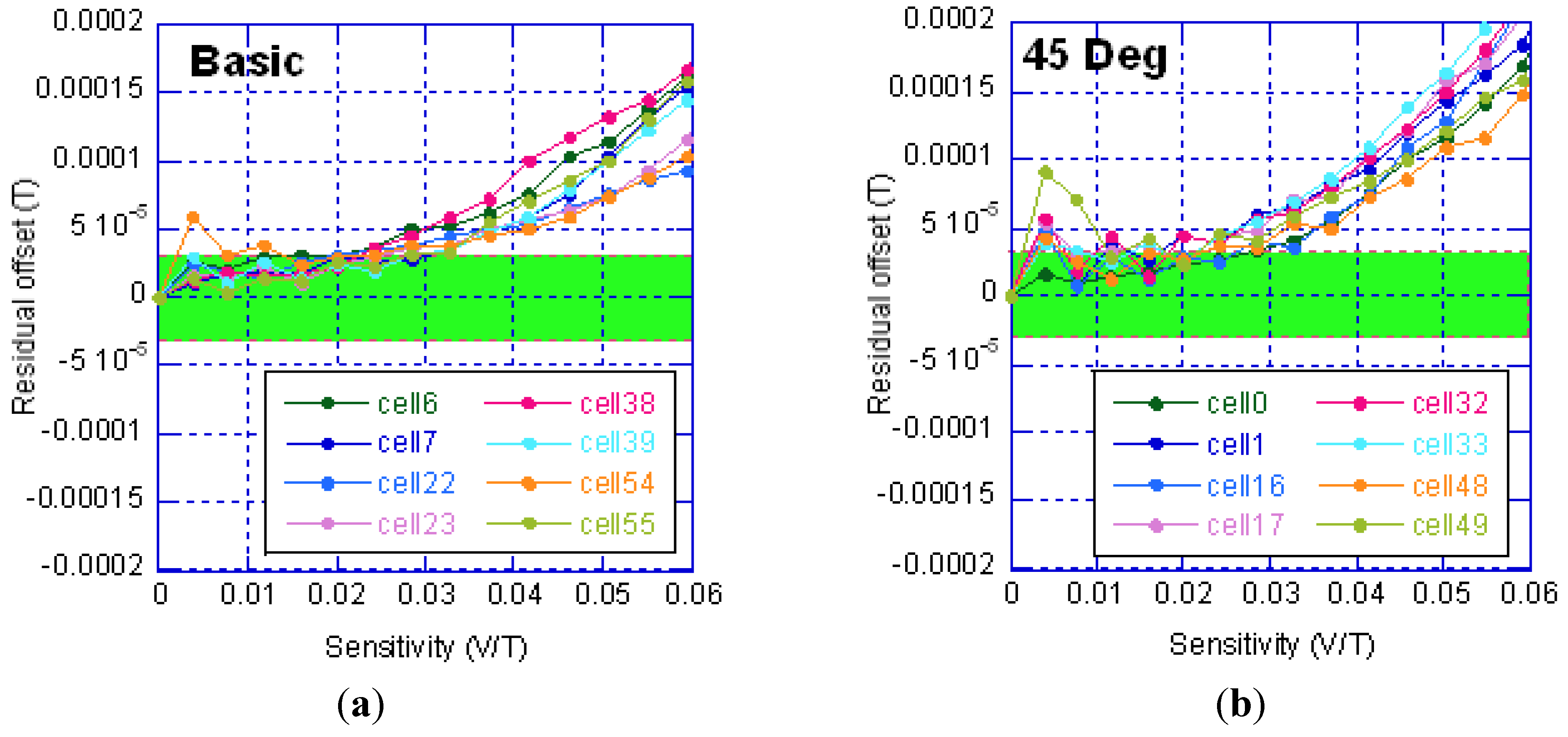
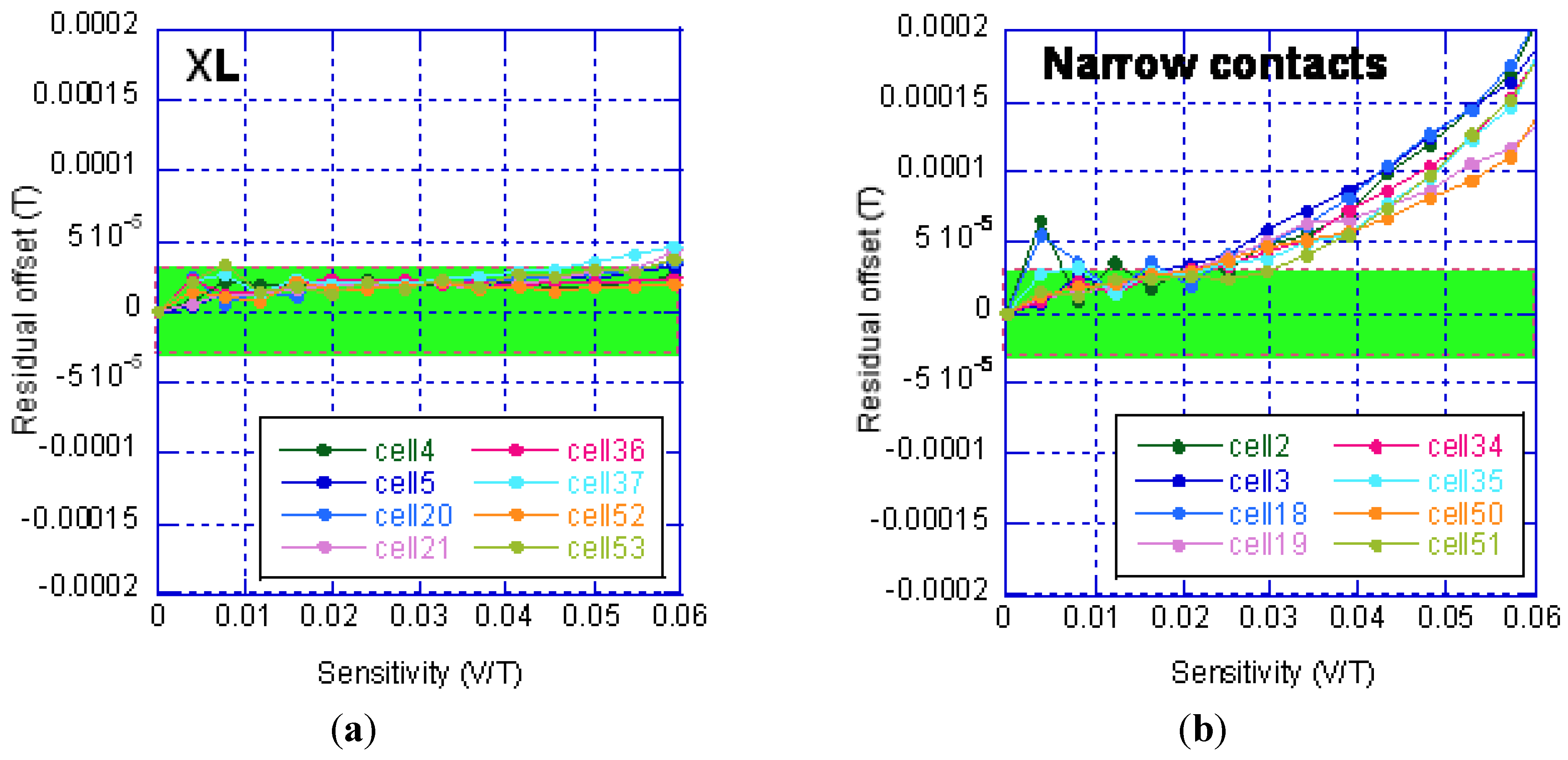
Figure 9,
Figure 10 present the 4-phases residual offset in T at room temperature
versus the absolute sensitivity for four of the integrated Hall cells. The indications in the legend represent the specific positions of the tested cell within a chip containing 64 cells. To obtain the data in
Figure 9,
Figure 10, the biasing current was ramped, and the residual offset measured. It is to be mentioned that the residual offset is not a direct function of the sensitivity, but an implicit one via the biasing current. However, for more meaningfulness, we decided to display this information
versus the absolute sensitivity, as it is useful to know how much residual offset corresponds to certain sensitivity.
Figure 9.
Room temperature residual offset for basic (a) and 45° (b) Hall cells.
Figure 9.
Room temperature residual offset for basic (a) and 45° (b) Hall cells.
Figure 10.
Room temperature residual offset for XL (a) and Narrow contacts (b) Hall cells.
Figure 10.
Room temperature residual offset for XL (a) and Narrow contacts (b) Hall cells.
By the green band we understand the project specifications in terms of offset at room temperature, which falls in the interval ±30 μT. We can observe that the best behavior is obtained for the XL cell.
4. Three-Dimensional Physical Simulations
Regarding Hall Effect sensors behavior analysis, a finite element lumped circuit model was recently developed by the authors in [
3]. Other models, based on six-resistance approach were proposed [
11].
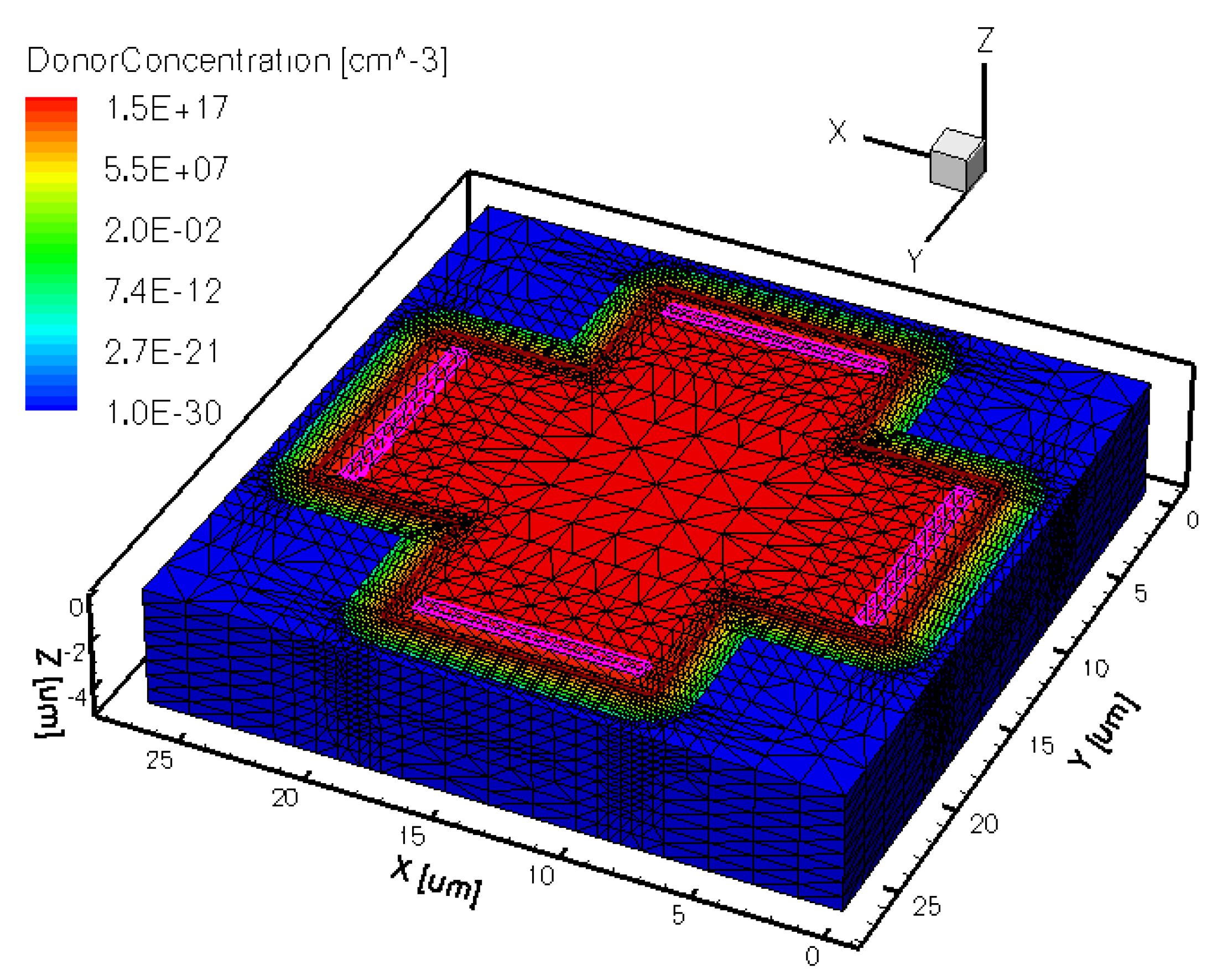
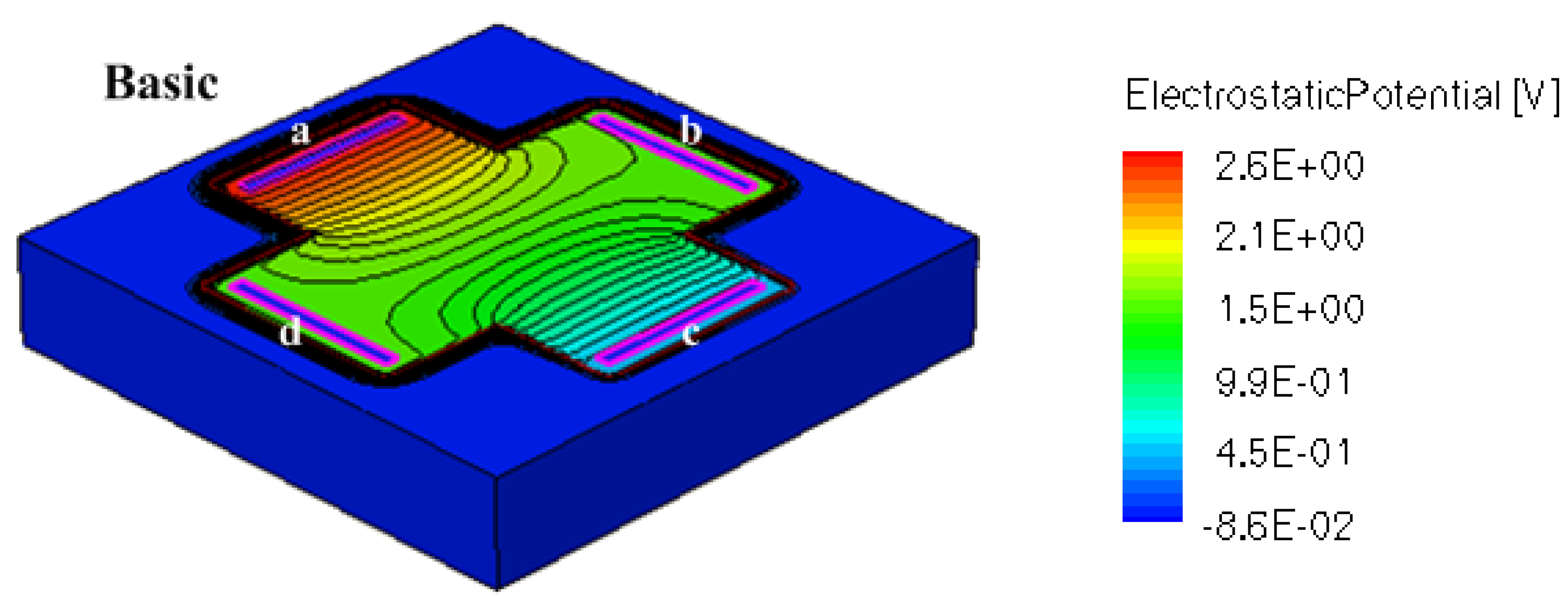
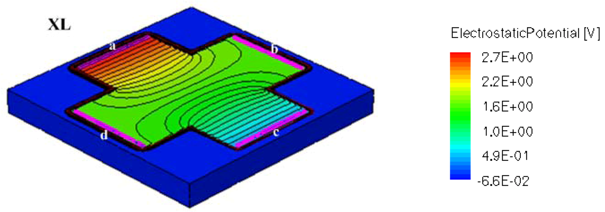
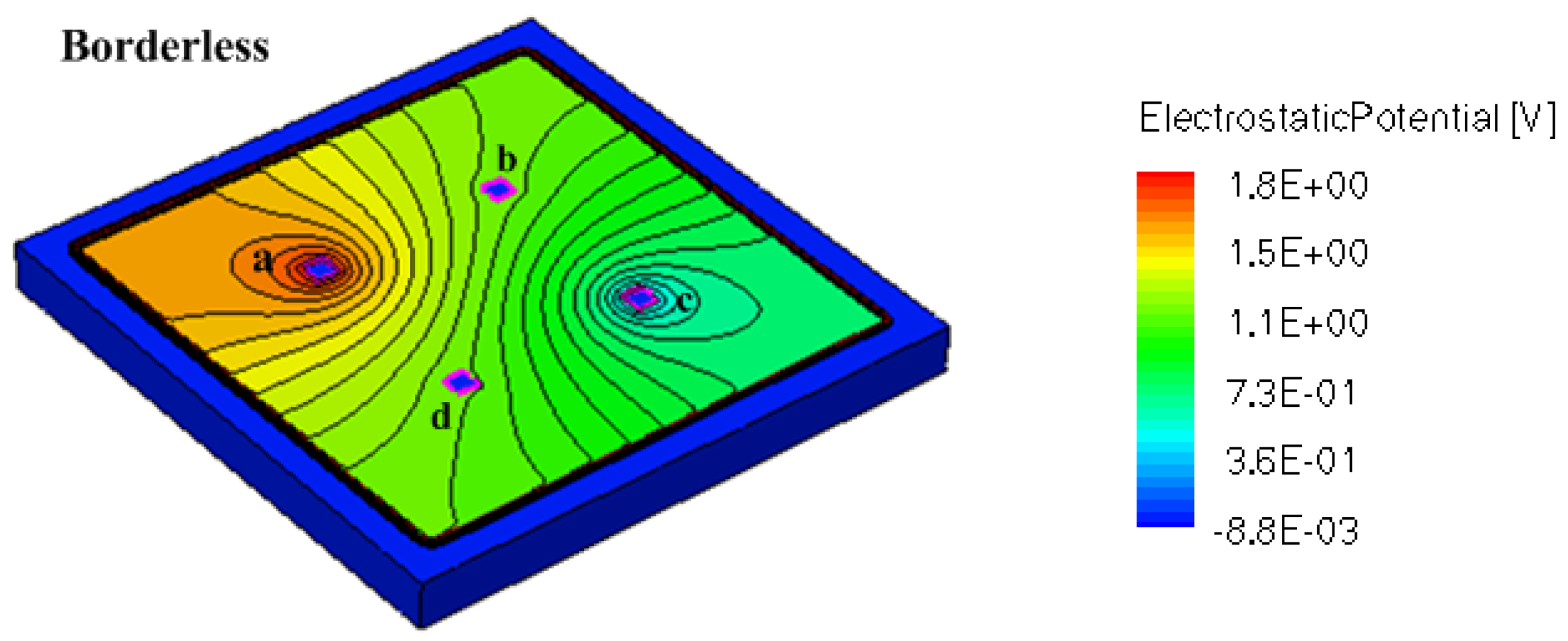
A powerful tool to predict the Hall Effect sensor’s performance is based on three-dimensional physical simulations. In a recent paper, the authors presented 3D simulations as an instrument to assess Hall sensors behavior [
12]. In this work, five different cells, including basic, L, XL, borderless, and optimum, were simulated and evaluated using TCAD Sentaurus Synopsys tool [
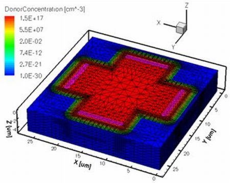
13]. In
Figure 11, the three dimensional structure of the basic cell with the donor concentration profile is displayed.
Figure 11.
Three-dimensional simulated structure of the basic Hall cell.
Figure 11.
Three-dimensional simulated structure of the basic Hall cell.
The structure is also endowed with four electrical contacts, located at the extremities of the arms. For the p-substrate, a Boron concentration of 1015 cm−3 is used while the active n-well region is implanted with an Arsenic doping concentration of 1.5 × 1017 cm−3 with a Gaussian profile. The thickness of the p-substrate is 5 μm while the n-profile implantation depth is 1 μm. In this case, the average mobility is 0.0630 m2·V−1·s−1.
5. Results and Discussion
The three-dimensional structures for three of the five simulated Hall cells are incorporated in
Figure 12,
Figure 13,
Figure 14, also depicting the electrostatic potential (V) distribution. A current in the range 0–1 mA was used to bias the Hall structures from
a to
c contacts and the Hall voltage was recorded between the opposite
b and
d contacts. For the cross Hall cells, the current has an orthogonal flow, while for the borderless and optimum cells, the current flow is on a diagonal path, according to
Figure 4. In
Table 3, the design parameters of the five simulated cells are summarized.
L,
W, and
s stand for sensors length, width, and sensing contacts length respectively.
Figure 12.
The three-dimensional representation of the simulated basic Hall cell.
Figure 12.
The three-dimensional representation of the simulated basic Hall cell.
Figure 13.
The three-dimensional representation of the simulated XL Hall cell.
Figure 13.
The three-dimensional representation of the simulated XL Hall cell.
Figure 14.
The three-dimensional representation of the simulated borderless Hall cell.
Figure 14.
The three-dimensional representation of the simulated borderless Hall cell.
Table 3.
Simulated Hall Effect devices geometrical parameters.
Table 3.
Simulated Hall Effect devices geometrical parameters.
| Hall Structure | L (μm) | W (μm) | s (μm) |
|---|
| Basic | 21.6 | 9.5 | 8.8 |
| L | 32.4 | 14.25 | 13.55 |
| XL | 43.2 | 19 | 18.3 |
| Borderless | 50 | 50 | 4.7 |
| Optimum | 50 | 50 | 2.3 |
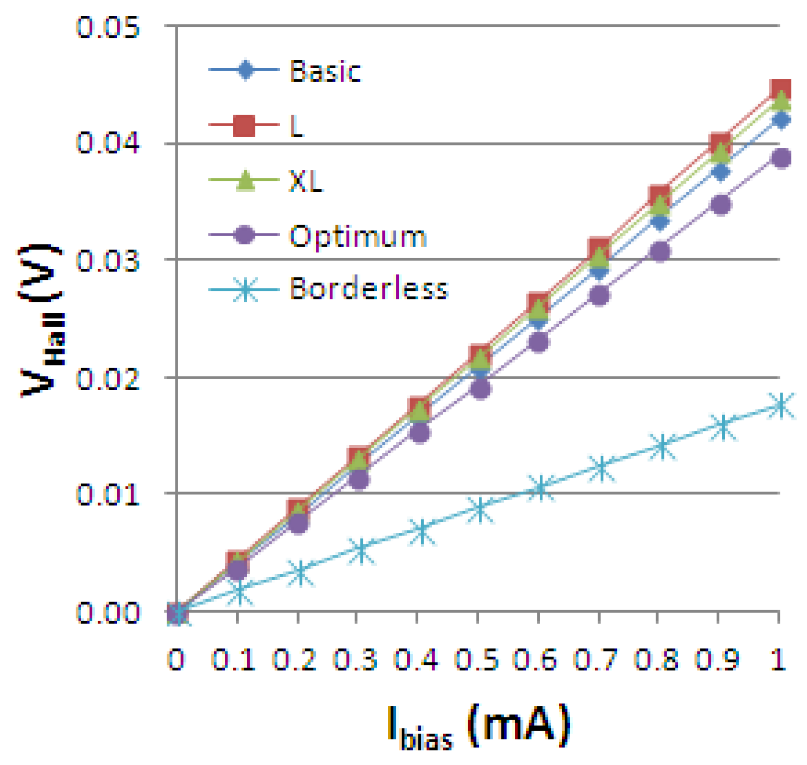
Figure 15.
Hall voltage (V) vs. biasing current for the five simulated Hall cells.
Figure 15.
Hall voltage (V) vs. biasing current for the five simulated Hall cells.
The five Hall cells were simulated for Hall voltage, by considering the influence of a magnetic field of strength B = 0.5 T. The following results were obtained as presented in
Figure 15.
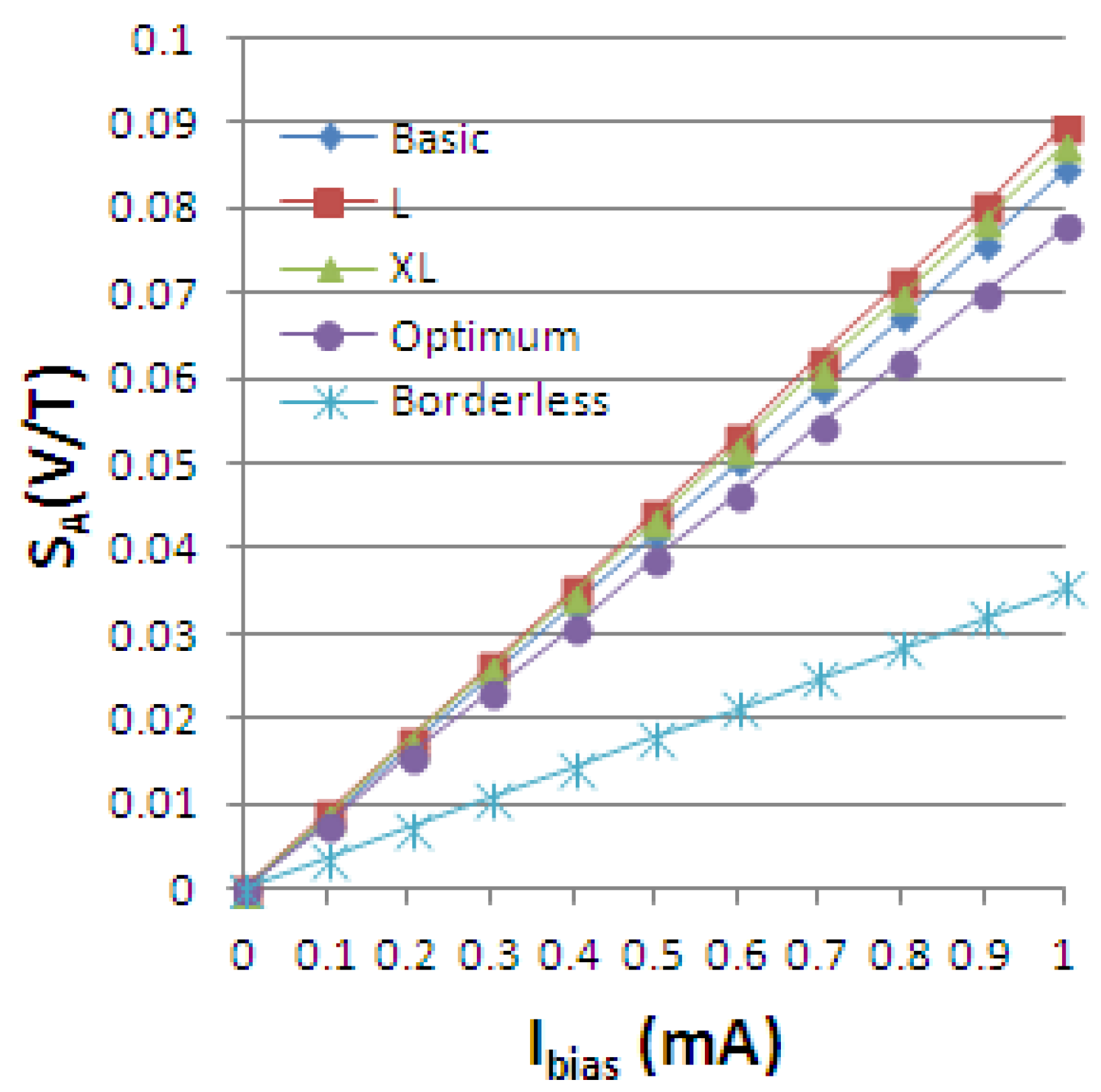
In
Figure 16, the absolute sensitivity
versus the biasing current is displayed for the five simulated Hall structures. We can observe that the cross Hall cells have the highest sensitivity, while there is a decrease in sensitivity for borderless and optimum cells, as confirmed by the measurements results presented in
Table 1.
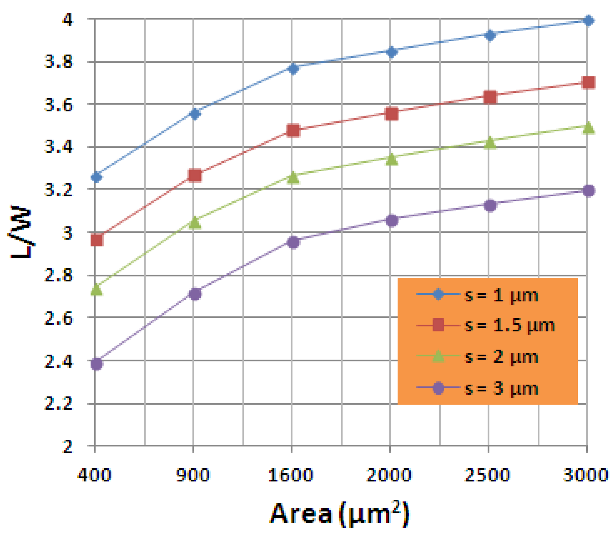
The sensitivity is directly related to the geometrical correction factor and G is in turn directly proportional to the length-to-width ratio. By consequence, it is expected for basic, L, and XL Hall cells to have approximately the same absolute sensitivity, as they are scaled up versions of a classical Greek-cross.
To explain the Hall voltage and sensitivity reduction in the square Hall cells compared to the cross structures, one has to take into consideration the geometrical correction factor G which is lower in the case of the square cells. Moreover, contacts on square structures located further away from the p-n junction considerably reduce the effective active n-well area, so they also produce a decrease in the sensitivity.
Figure 16.
Absolute sensitivity (V/T) vs. biasing current for the five simulated Hall cells.
Figure 16.
Absolute sensitivity (V/T) vs. biasing current for the five simulated Hall cells.
6. Conclusions
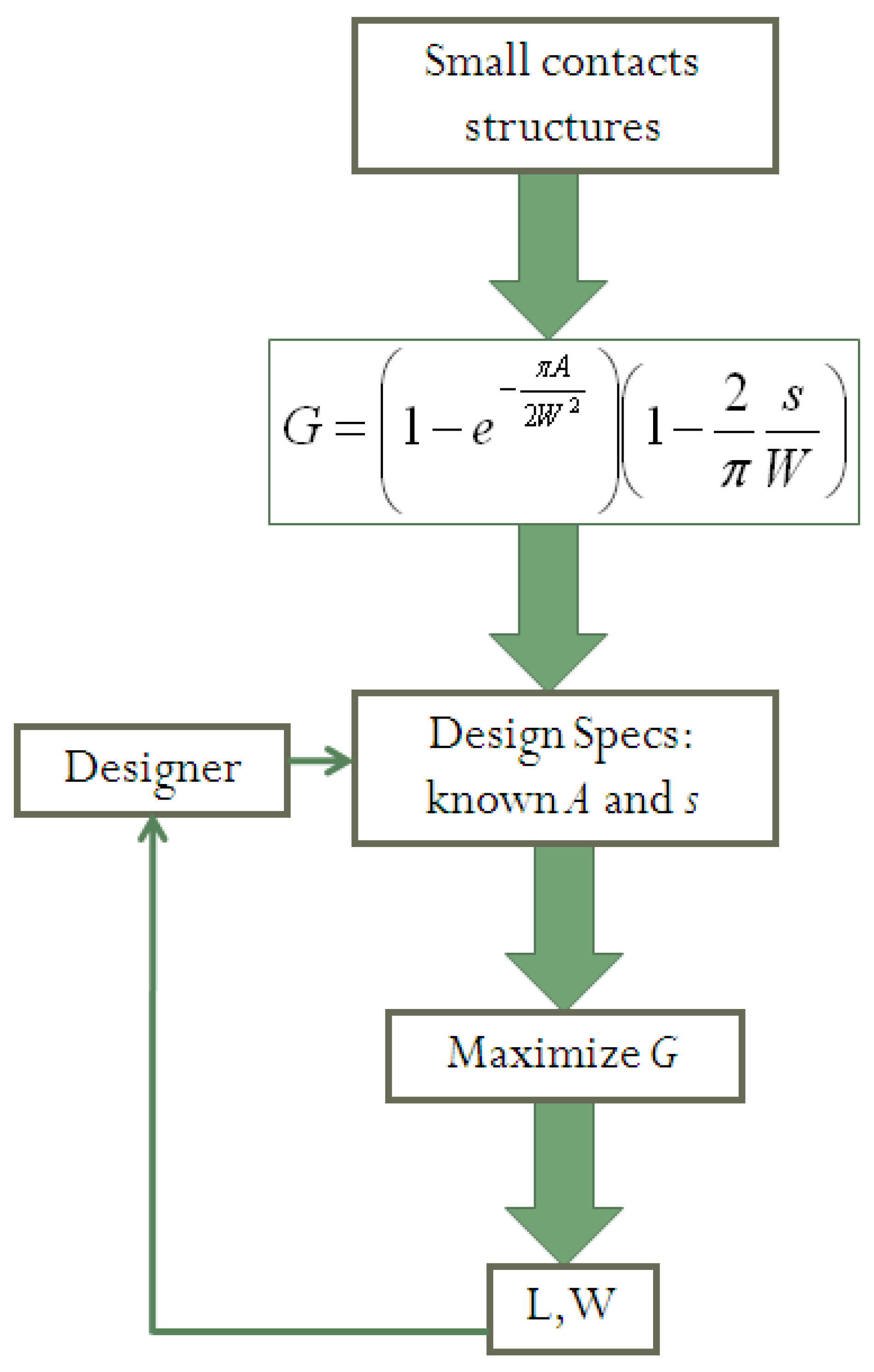
Different Hall effect sensors were integrated in a CMOS technology, and their performance, were evaluated. The measurements results corresponding to the sensitivity, residual offset, and its behavior with the temperature were presented, with a comparative analysis on different Hall cell types. To achieve the highest sensitivity, geometrical correction factor maximization was performed for long rectangular Hall structures with small sensing contacts. To model the Hall Effect sensors behavior and predict their performance, three-dimensional physical simulations were performed. This procedure can guide the designer in selecting the best integration process, adequate Hall cell shapes and dimensions.


 , where
  is the length of the arms.
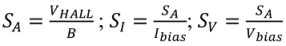
