Article

An Area-Efficient and Programmable 4 × 25-to-28.9 Gb/s Optical Receiver with DCOC in 0.13 µm SiGe BiCMOS

1
Institute of Astronautic Electronic Engineering, School of Aeronautics and Astronautics, Zhejiang University, Hangzhou 310007, China
2
Institute of Advanced Technology, Zhejiang University, Hangzhou 310007, China
*
Author to whom correspondence should be addressed.
Electronics 2020, 9(6), 1032; https://doi.org/10.3390/electronics9061032
Submission received: 10 May 2020 / Revised: 8 June 2020 / Accepted: 17 June 2020 / Published: 22 June 2020
(This article belongs to the Special Issue Advanced Integrated Circuits Technology)

Abstract

:
In this paper, we present an area-efficient noise-optimized programmable 4 × 25-to-28.9 Gb/s optical receiver. Both high- and low-power modes are available for the receiver to meet different requirements. Emitter degeneration provides the input transimpedance amplifier (TIA) stage with improved stability. The noise of the TIA with emitter degeneration is analyzed, and an improved noise optimization method for the TIA is proposed. A sink current source with emitter degeneration in a DC offset cancellation (DCOC) loop reduces the noise introduced by the DCOC circuit. Moreover, with parasitic capacitor utilization in the DCOC loop and capacitive emitter degeneration in the variable-gain amplifier (VGA) stage, the chip area is minimized. Fabricated in a 0.13 µm SiGe BiCMOS technology, the receiver achieved a small area of 0.54 mm2 per lane. The measured bit error rate (BER) is 10−12 with input signal varying from 110 μApp to 1150 μApp. The one-lane power dissipation values in the low-power and high-power modes are 84.97 mW and 123.75 mW, respectively.

1. Introduction

The exponential growth of data traffic has created higher data rate requirements for electronic components [1]. To meet the increasing demand among computational blocks, communication links with data rates exceeding hundreds of Gb/s [2] are needed. Compared with telecommunication, multilane optical communication [3] has been widely used for its excellent capability [4].
In previous research, several multilane optical receivers with high-speed data rates and noise optimization have been developed [5,6,7,8,9,10,11] in CMOS and SiGe BiCMOS technology. A multilane optical receiver with data rates exceeding hundreds of Gb/s was first functionally realized by Shibasaki, T. [2] in 2015. In order to explore performance enhancement of the optical receivers, a wide-band design of the receivers was analyzed by Kokolov, A.A. [12] in 2019, a noise optimization method was proposed by Li, D. [9] in 2016, and power and area reductions in advanced CMOS technology were made by Shahramian, S. [13] in 2019. However, there still exist some shortcomings which need to be improved in these receivers, such as bad compatibility with more than one specific operating mode; complicated trade-offs among stability [14], bandwidth, and noise [9] of the input transimpedance amplifier (TIA) stage; and high manufacturing costs due to the large chip area in SiGe BiCMOS technology, etc.
In this paper, we present an area-efficient noise-optimized programmable 4 × 25-to-28.9 Gb/s optical receiver for a multilane optical fiber system in 0.13 μm SiGe BiCMOS. With a flexible power mode and received signal strength indication (RSSI) function, the proposed optical receiver works at 4 × 25-to-28.9 Gb/s data rates and provides variable gain and output swing, etc. In order to avoid intersymbol interference (ISI) for instability of the input TIA stage, the stability of the input TIA stage is improved with the introduction of emitter degeneration. Meanwhile, a noise model of the input TIA stage with emitter degeneration is analyzed. Then, an improved noise optimization method based on the noise model and parameter scaling is proposed. As a result, complicated trade-offs among noise, bandwidth, stability, and S11 (scattering parameters) are avoided. To reduce the chip area, the capacitors in the lowpass filters of the DC offset cancellation (DCOC) loop are omitted due to parasitic capacitor utilization and capacitive emitter degeneration, rather than the commonly used large-sized passive inductors, applied to bandwidth extension in the variable-gain amplifier (VGA) stage. Additionally, the sink current source with emitter degeneration reduces the input-referred noise of the receiver which is introduced by the DCOC circuit.
This paper is organized as follows. The chip architecture is introduced first in Section 2. Then, detailed circuit designs are presented in Section 3, followed by the measurement results in Section 4. Finally, conclusions are drawn in Section 5.

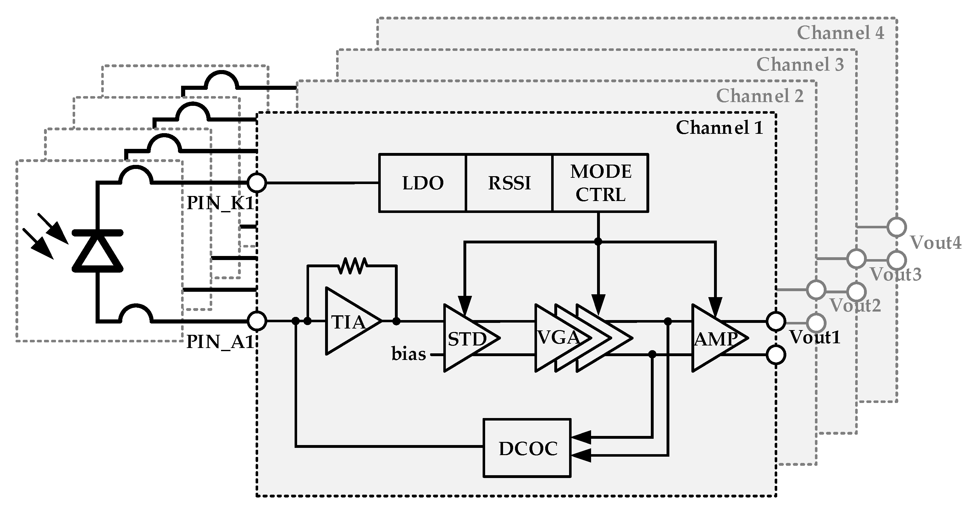
2. Architecture Design

Figure 1 presents the detailed architecture of the optical receiver with four parallel lanes. PIN_Kx (x = 1, 2, 3, 4) are the output pads of the four-lane on-chip low dropout regulators (LDOs), which are connected to the cathodes of the photodiodes by bonding wires to provide clean bias. PIN_Ax (x = 1, 2, 3, 4) are the input pads of the four lanes, which are all connected to the anodes of the photodiodes by bondwires. Furthermore, the series inductance introduced by the bondwire helps to isolate the photodiode capacitor from the TIA input capacitor [15]. Additionally, Voutx (x = 1, 2, 3, 4) is the differential pad for the output of lane x.
Each lane of the optical receiver contains a TIA, a single-ended–differential amplifier (STD), a VGA, an output amplifier, a DCOC loop, and an RSSI module. At the input stage, the TIA is designed to preamplify the small current signal to a large voltage signal. Then, the STD stage converts the single-ended voltage signal to a differential signal. The VGA amplifies the voltage signal to a level which is sufficient for the reliable operation of other subsequent implements [16]. Finally, the output amplifier at the output stage drives the off-chip load.
The DCOC loop is implemented to eliminate the output DC offset due to process variation [17]. Additionally, the RSSI module is applied to control the adjusting resistors in the VGA, which changes the photodiode’s DC current provided by the LDO on the chip. Furthermore, adjustment of the output swing, gain, and bandwidth is realized by controlling the current sources of the STD, the VGA, and the output amplifier via the power mode controller. The four lanes share only one bandgap module on the chip in order to minimize the chip area.

3. Circuit Design

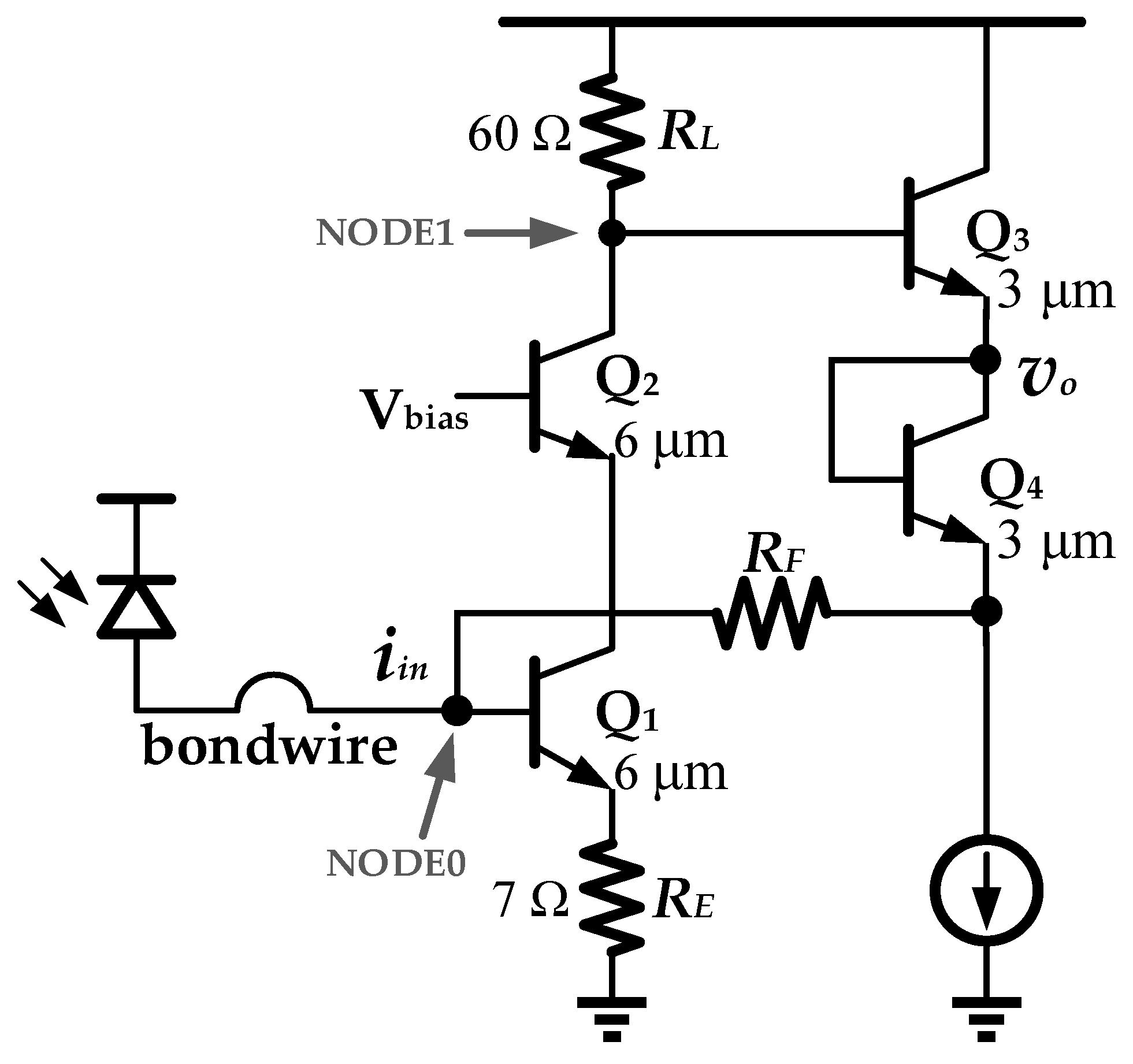
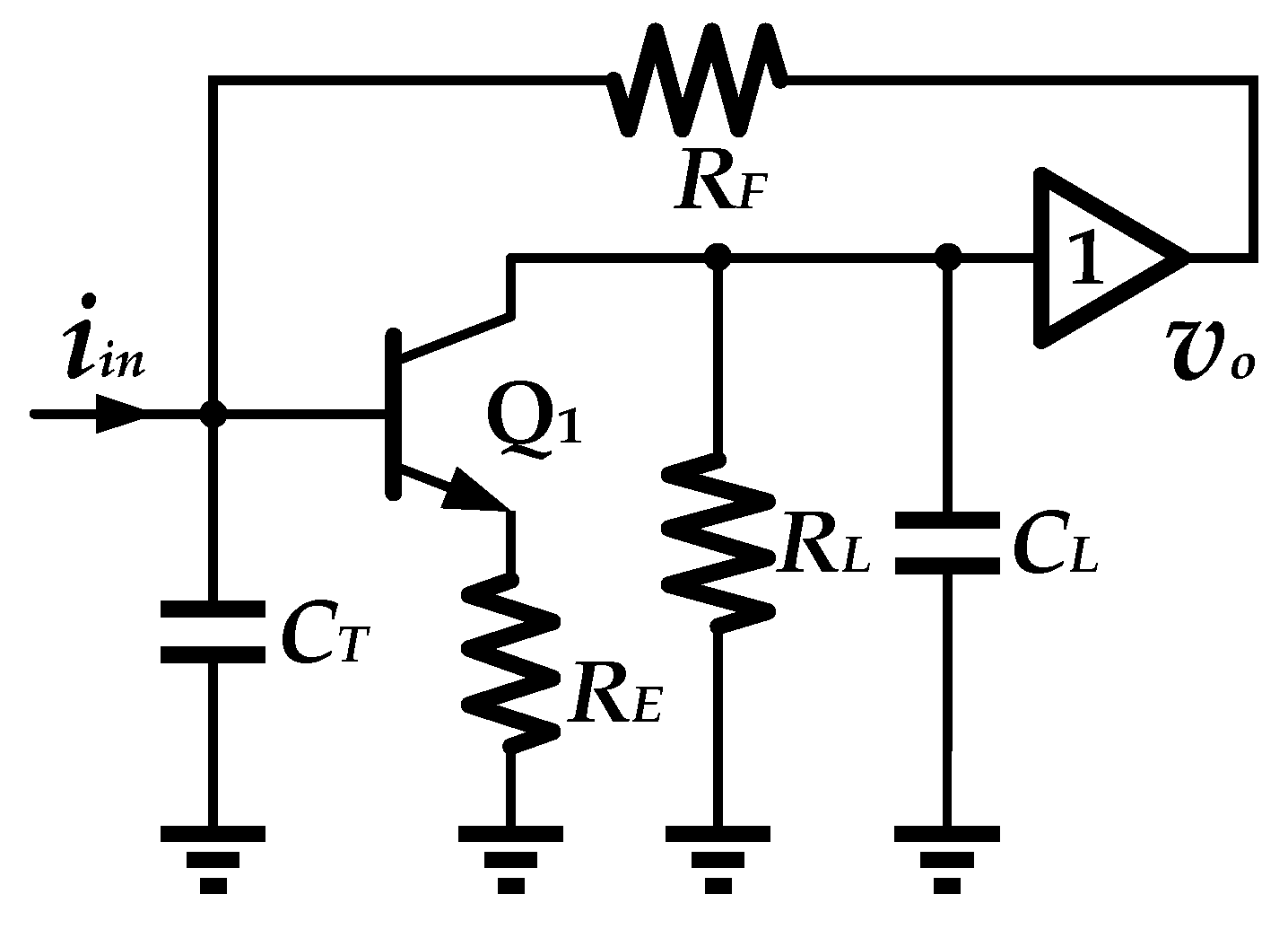
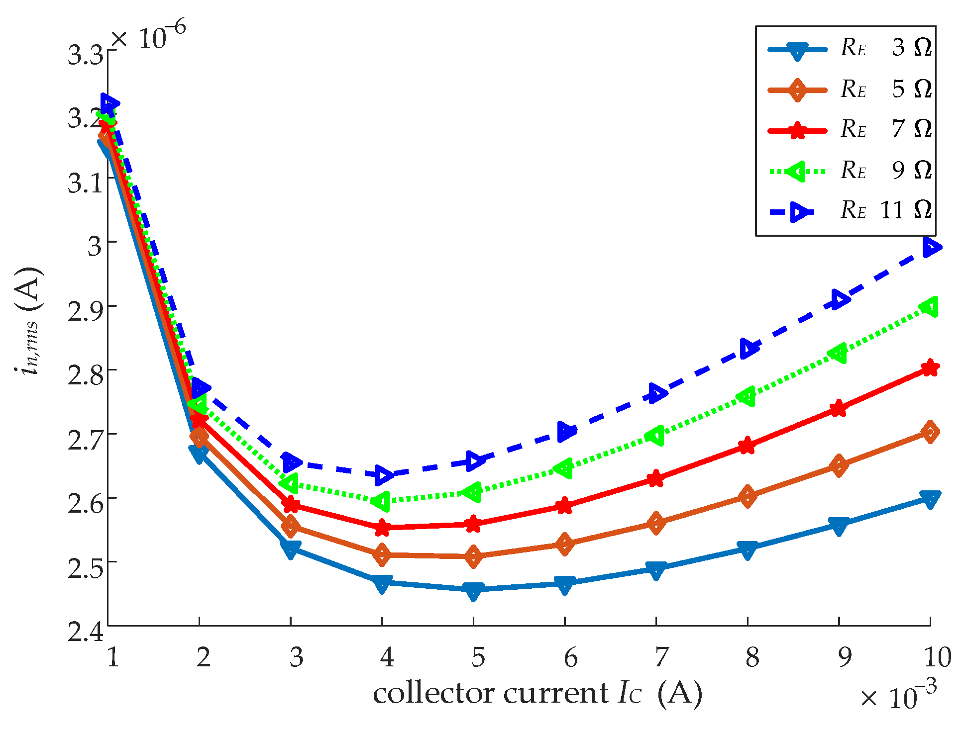
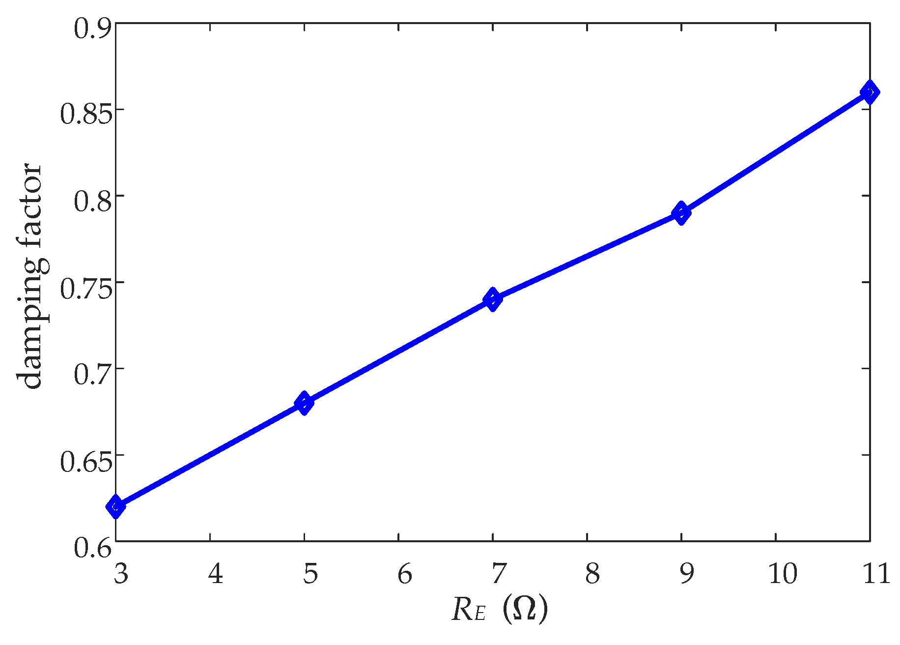
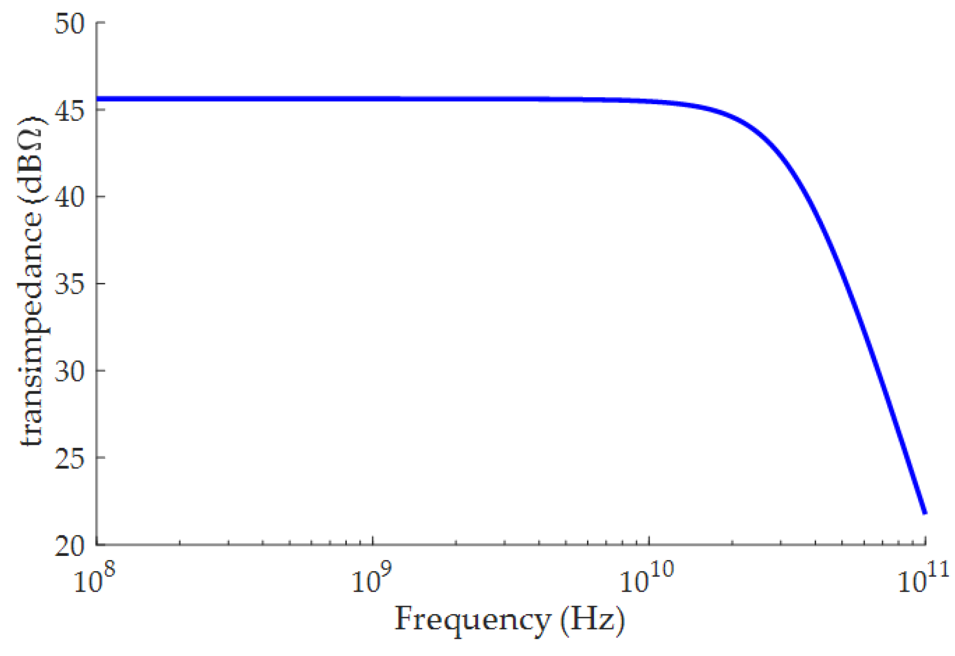
3.1. Transimpedance Amplifier

As shown in Figure 2, a single-ended shunt–shunt feedback TIA architecture with emitter degeneration followed by a cascode configuration was designed. The feedback resistor RF provides a good trade-off between the low noise and wideband characteristics of the TIA [18]. It is necessary to insert cascode Q2 for better isolation and to avoid excessive collector–emitter voltage, followed by an emitter follower Q3 for the sake of driving the next stage. Considering that the input voltage of TIA is around 1 V, a level-shift circuit is needed in the feedback loop. Therefore, a diode-connected bipolar transistor, Q4, is inserted into the feedback loop in series for level shifting, which saves the power by avoiding the introduction of an additional emitter follower stage for level shifting. Considering the ISI and harmonic distortion due to bad linearity, a tantalum nitride resistor with good linearity was chosen as RF to avoid the degradation of deterministic jitter.
An ideal TIA must satisfy the requirements of low noise, high gain, relatively wide bandwidth, and small deterministic jitter. Hence, there is an inevitable trade-off [19] among them, and a circuit model is helpful to optimize the TIA. Considering the time constants of the nodes in the TIA feedback loop, the input pole (NODE0) of the TIA and the output pole (NODE1) of common emitter (CE) stage Q1 with emitter degeneration dominate the bode plot of the TIA feedback system. Meanwhile, the capacitance at the input node of the optical receiver has the largest value among all the nodes, which provides the largest time constant and leads to the dominant pole. Thus, the small-signal equivalent circuit of the input TIA can be simplified into a second-order system, which is shown in Figure 3.
The transfer function of the simplified small-signal equivalent circuit is derived as
v o u t i i n = g m R L ( 1 + g m R E ) C T R L C L s 2 + R F C T + R L C L R F C T R L C L s + R F C T + R L C L ( 1 + g m R E ) R F C T R L C L ,
where CT denotes the total input capacitance and gm denotes the transconductance of Q1. CT consists of CEX (the capacitance of the pad, the photodiode) and Cb (the input capacitance of Q1). Derived from Equation (1), the damping factor ξ of the input TIA is given by
ξ = 1 2 C T R F R L C L + 1 g m R L C T R F ( 1 + g m R E ) R L C L .
As Equation (2) shows, ξ is improved by the emitter degeneration term gmRE, i.e., the stability of the input TIA, and ξ must be larger than 0.71 for PVT (process voltage temperature) variation. Assume that 1/(RLCL) is larger than the bandwidth of the input TIA stage BW; then BW is given by
B W = g m R L 1 + g m R E 1 R F C T = A V R F C T .
The −3 dB bandwidth (BW) of the input TIA commonly depends on the input pole [20] and the gain (AV) of CE stage Q1 with emitter degeneration from Equation (3). Considering that the bandwidth requirement of the input TIA is 0.7 times the data rate [21], the value of AV is derived from given RF and CT.
Considering the noise of the optical receiver, the noise of the first stage (the input TIA) dominates the noise performance [22]. With the given requirement of ξ and BW, optimum performance of the input TIA can be obtained by optimizing the noise. Moreover, the 1/f noise of the transistors in Figure 2 is ignored for high-speed applications, such that the thermal noise dominates [23]. The thermal noise of the CE stage and RF contributes most to the total noise of the TIA without emitter degeneration [24]. With the introduction of emitter degeneration, shown in Figure 2, the input-referred noise voltage spectrum of CE stage Q1 with emitter degeneration v n , C E 2 ¯ is expressed as
v n , C E 2 ¯ = 4 k T ( r b + 1 2 g m + R E ) ,
where rb is the base resistor of Q1. Then the input-referred noise current spectrum i n , i n 2 ¯ of the input TIA is given by
i n , i n 2 ¯ = ( i i n v i n ) 2 v n , C E 2 ¯ + 4 k T R F = 4 k T ( r b + 1 2 g m + R E ) 1 + s 2 ( R F C T ) 2 R F 2 + 4 k T R F .
There are two terms in Equation (5); the first term is the shaped noise (f2 noise) of CE stage Q1 with emitter degeneration, while the second term is the noise introduced by RF. There are inevitable trade-offs between the five parameters in Equation (5) for noise optimization, namely, rb, gm, RE, RF, and CT. However, conventional noise optimization methods [9] have several shortcomings: the noise introduced by RE is not considered, nor are the relationships among IC (the collector current of Q1), rb, gm, and CT. With multiple parameters to trade off, the conventional noise optimization method is complicated.
Considering that the performance of the bipolar transistor varies a lot with the DC operating point in SiGe BiCMOS technology, Q1 with given size has to be biased at the optimum operating point for high Ft (characteristic frequency) and β (common emitter current gain). Therefore, the size of Q1 can be determined by a given IC. Then, the sizes of Q1, Cb, and gm are proportional to IC [25], and Rb is inversely proportional to the sizes of Q1 and IC. Hence, IC determines the values of rb, gm, and CT with given CEX. The improved noise optimization method modifies the noise model (Equation (5)) and gets the relationships among IC, rb, gm, and CT; then the optimum IC can be obtained from given RF, RE, and CEX.
As a rule of thumb, the value of CEX is 100 fF. As given by Equation (5), the noise is also suppressed by large RF. However, large RF would degrade the bandwidth of the TIA from Equation (3) and S11. As a result of a trade-off, RF was selected to be 230 Ω. Although the noise and crosstalk coupled from the ground wire are suppressed by emitter degeneration, the noise introduced by emitter degeneration resistor RE increases the input-referred noise current of the input TIA stage. Therefore, the value of RE has to be small enough that it will not deteriorate the input-referred noise. The results of the noise optimization method by Matlab with RE varying from 3 Ω to 11 Ω are shown in Figure 4. Considering the requirement of ξ, RE was selected to be 7 Ω from Figure 5. Then, the optimum collector current is 4 mA, and the corresponding emitter length of Q1 is 6 μm. The value of AV was derived from the given RF and CT from Equation (3) for the bandwidth requirement. As shown in Figure 6, the simulated BW of Figure 2 is 29 GHz. Meanwhile, the simulated in,rms of Figure 2 is 2.6 μA, which confirms the accuracy of the noise model in Equation (5) and the improved noise optimization method. With the stability of the TIA enhanced by emitter degeneration, the simulated damping factor ξ (Equation (2)) is 0.74, which is stable enough for PVT variation.

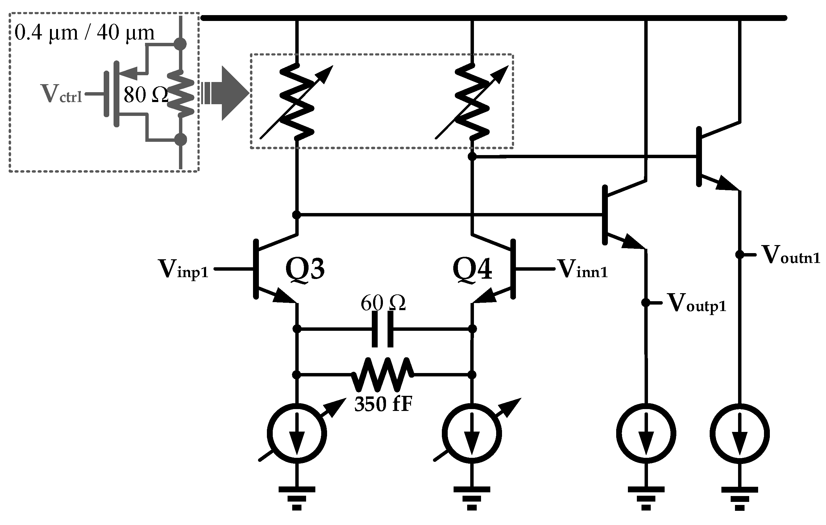
3.2. Single-Ended–Differential Amplifier

The current signal from the photodiode is a unipolar non-return-to-zero (NRZ) single-ended signal. Compared with a single-ended signal, a differential signal offers superiority [26] that makes it the optimal choice for signal processing. The STD stage following the input TIA stage transforms the single-end signal to a differential signal. The STD stage block diagram is shown in Figure 7.
A common differential amplifier with cascode structure and a variable current source comprises the STD stage. The variable current source controlled by the power mode equips the STD stage with variable gain. The differential inputs of the STD stage are the output of the input TIA stage and a DC bias generated by a dummy TIA. Meanwhile, the bias is set equal to the output DC component of the TIA stage. Then, the phase and amplitude discrepancy in differential signals can be minimized with this structure. As shown in Figure 8a,b, the simulated gain and phase discrepancy of the optical receiver are smaller than 0.05 dBc and 0.4° within the bandwidth of interest, respectively, which provides good matching performance.

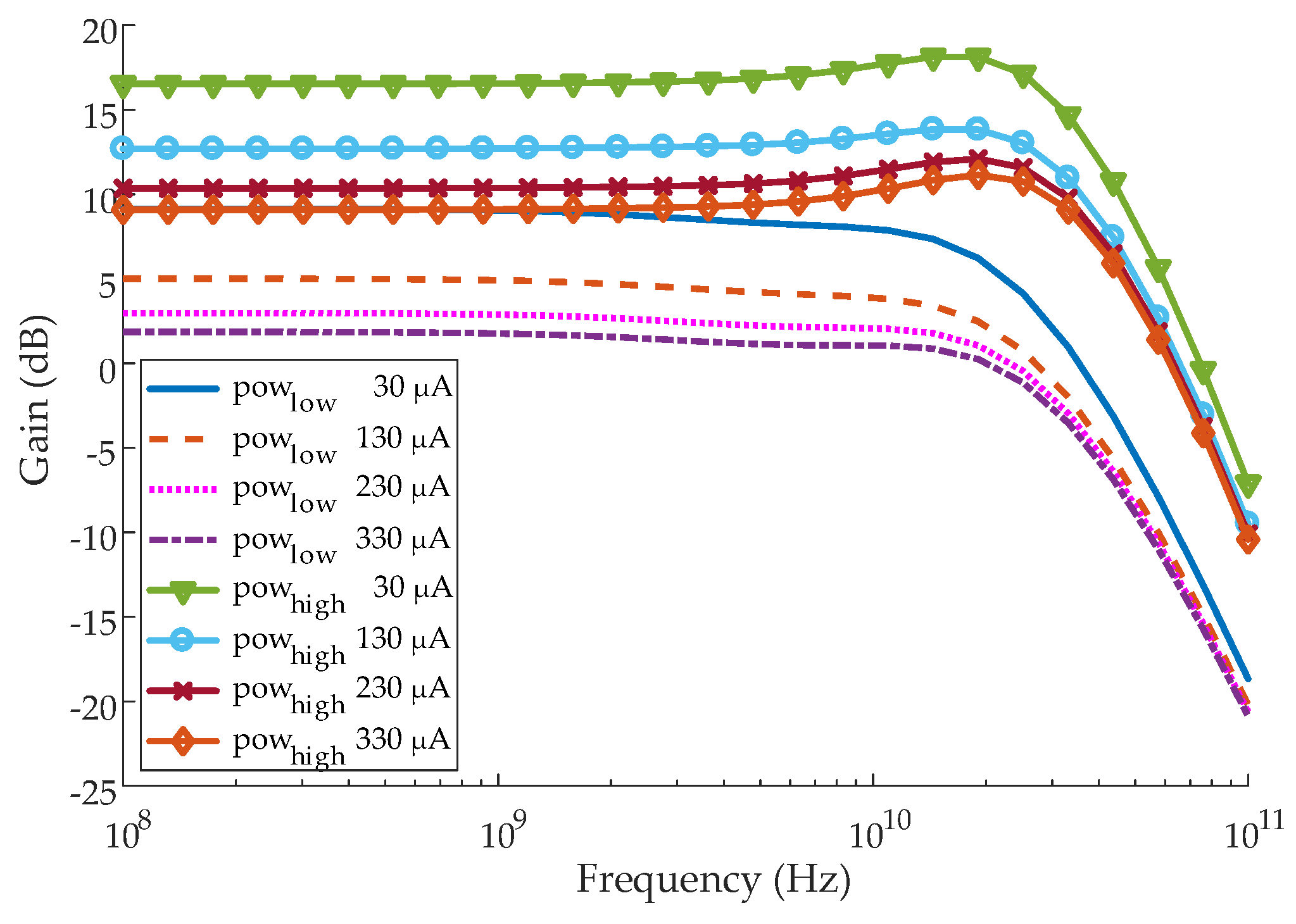
3.3. Variable-Gain Amplifiers

Optical receivers with enough gain assure the signal for other subsequent reliable implements. The two-stage VGA provides the optical receiver with high gain. A schematic of each stage is given in Figure 9. A complete schematic of the one-stage VGA consists of the capacitive degeneration structure, two adjusting load resistors, and two identical variable current sources.
The adjusting resistor consists of a fixed resistor and a PMOS. The PMOS transistors controlled by Vctrl in Figure 9, created by the RSSI module in Figure 1, act as variable resistors. Then, the PMOS resistors vary with the LDO output current, which denotes the input signal strength. Since it is unaffordable to extend the bandwidth by using inductors for area minimization, capacitive degeneration as an active inductor was applied for bandwidth extension. The variable current source controlled by the power mode equips the VGA stage with variable gain. Each VGA stage is followed by an emitter follower stage to drive the next module. Finally, the simulated two-stage VGA frequency response with different LDO output currents in low-power mode and high-power mode is shown in Figure 10. The simulated gain of the VGA varies from 16.5 dB to 9.1 dB in high-power mode, and the gain of the VGA varies from 9.1 dB to 1.8 dB with the current reduced in low-power mode.

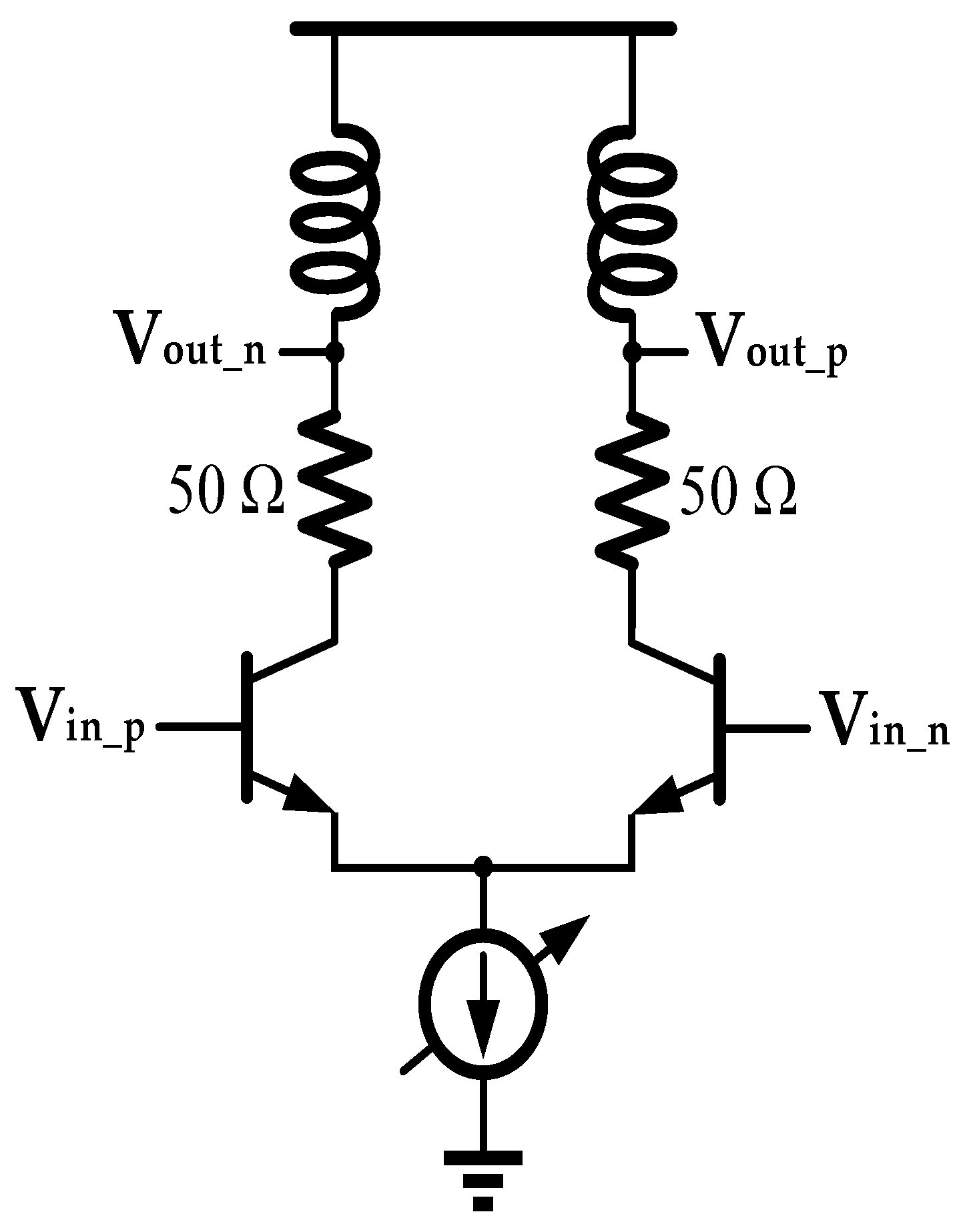
3.4. Output Amplifier

A schematic of the output amplifier is shown in Figure 11. The bandwidth of the output stage is limited by unavoidable large parasitic capacitance. An inductor is used in the output stage to compensate the effect of this parasitic capacitance. The inductance in series with a resistor creates zero peaking for bandwidth extension. The adjusting current source is programmable for variable output swing. In order to get a much cleaner eye diagram with high eye height, the current source was set with large output current in the high-power mode. The simulated 25 Gb/s and 28.9 Gb/s eye diagrams of the optical receiver in high-power mode are shown in Figure 12a,b, and the simulated 25 Gb/s and 28.9 Gb/s eye diagrams of the optical receiver in high-power mode are shown in Figure 13a,b. The simulated eye heights in high-power mode and low-power mode are 255 mV and 90 mV, respectively. The eye height also decreases with higher data rates.

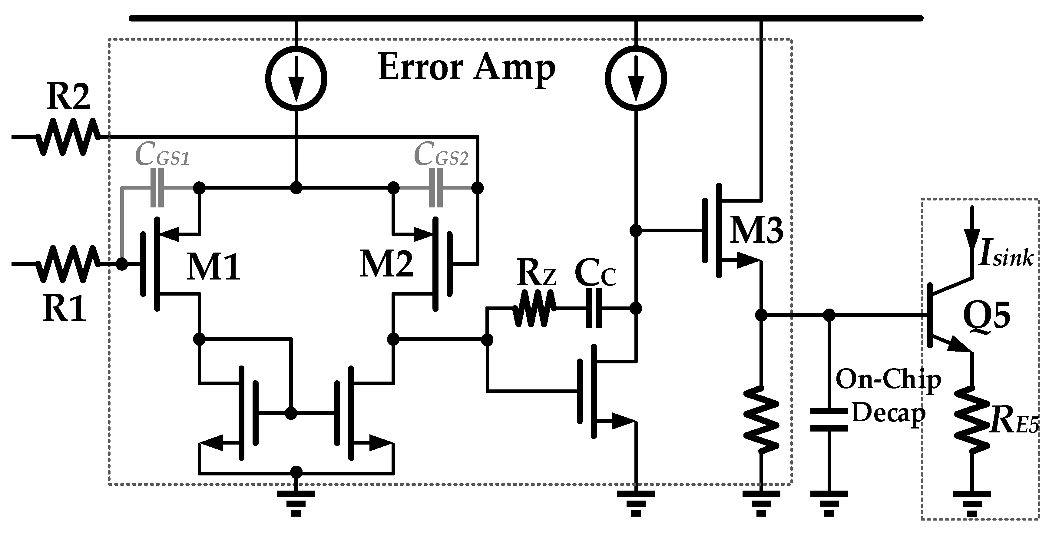
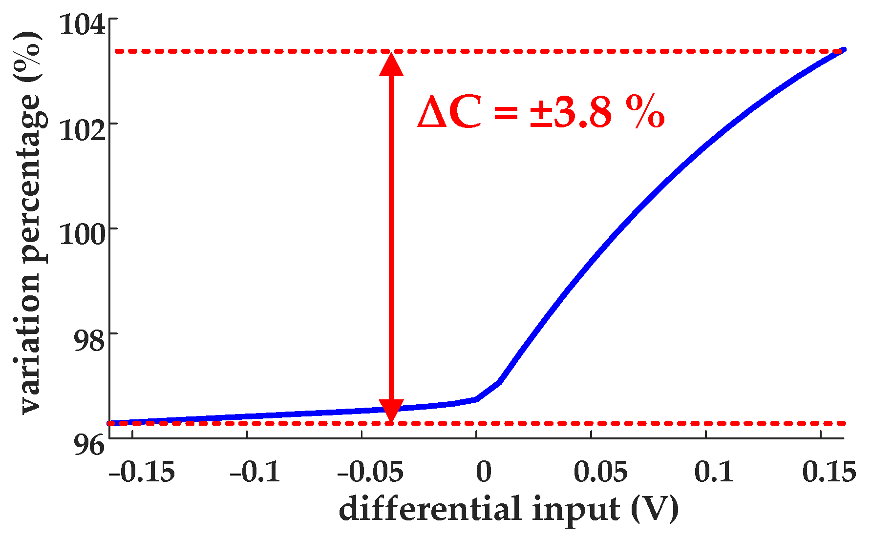
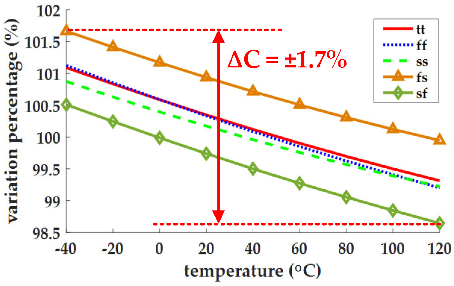
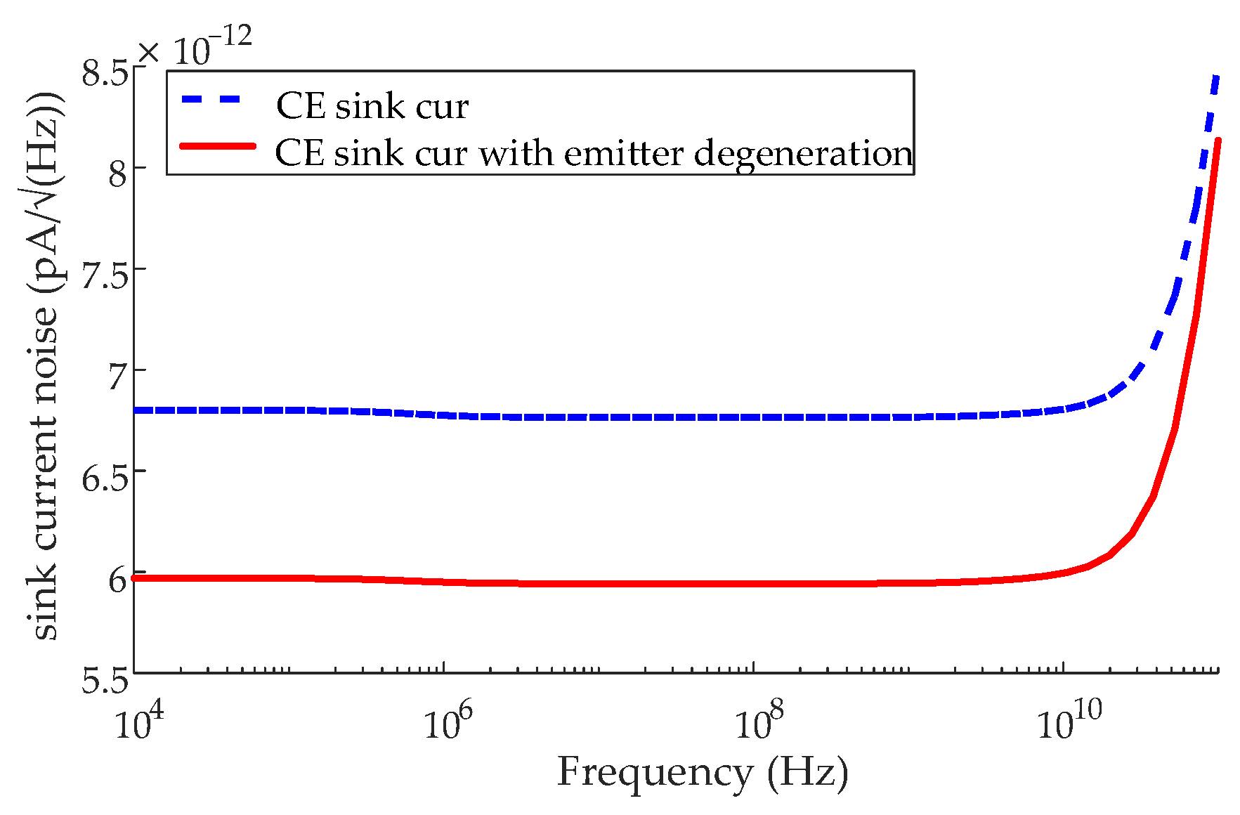
3.5. DC Offset Cancellation Loop

There are a large number of nonideal factors that can increase the output offset, such as inevitable device mismatch, large gain of the receiver, flicker noise, the sink current of the photodiode, and PVT variation. Therefore, a DCOC circuit following the VGA stage [27] was designed to eliminate the output offset.
As shown in Figure 14, the schematic of the DCOC circuit consists of a lowpass filter, an error amplifier, and a sink current source. The DCOC circuit should extract the offset signal from the output of the VGA stage without data signal deterioration. Therefore, lowpass filters with large resistors are commonly implemented as the first stage in a DCOC circuit.
The bandwidth of the lowpass filter in a DCOC loop is typically designed to be a few megahertz. The capacitance density of a nitride metal-insulator-metal (MIM) capacitor is around 0.001 mm2/pF in 0.13 μm SiGe BiCMOS technology. The area of the capacitors is about 0.032 mm2 to realize the typical 4 MHz bandwidth of a lowpass filter with given R1 and R2.
In our design, the DCOC loop without the capacitors of the lowpass filter can also realize the function of DCOC (DC offset cancellation), and the bandwidth (BW) and the gain–bandwidth product (GBW) of the DCOC loop remain unchanged. Due to the high-swing input signal, the error amplifier in a DCOC loop would work improperly without parasitic capacitors. Finally, parasitic capacitors result in a 6% decrease in chip area by avoiding the introduction of the additional capacitors in a typical design.
As shown in Figure 15 and Figure 16, the variations of the total parasitic capacitance in the following error amplifier (the sum of CGS1 and CGB1) which caused by differential input voltage, process and temperature are smaller than 3.8% and 1.7%, respectively. The PVT variation of the parasitic capacitors is too small to affect the DCOC loop; hence, the PVT variation of the parasitic capacitors can be considered acceptable.
An error amplifier following the lowpass filter was implemented to amplify the DC offset. The effective value of CC becomes large due to the Miller effect; then the dominant pole of the error amplifier is pushed to low frequency, which avoids the data signal coupling from the VGA stage to the input TIA stage through the DCOC loop. The simulated coupling isolation is about −128 dBc at 12.5 GHz.
The DCOC loop shown in Figure 1 is based on feedback architecture [28], and the transfer function of the DCOC loop is given by
H D C O C = H A M P ( s ) 1 + H A M P ( s ) H e r r o r ( s ) g m 5 1 + g m 5 R E 5 ,
where HAMP(s) denotes the transimpedance transfer function from the input TIA to the VGA stage, Herror(s) is the transfer function of the error amplifier in the DCOC circuit, and gm5 is the transconductance of Q5. Considering that HAMP(s) and Herror(s) are far more than 1 within the bandwidth of the DCOC loop, HDCOC(s) << 1, and the DC offset and flicker noise are attenuated by the feedback architecture from Equation (6).
Considering the input-referred noise of the optical receiver deteriorated by the DCOC loop, the input-referred noise introduced by the error amplifier and the sink current source were analyzed. The input-referred noise current of the optical receiver contributed by the error amplifier in,in_error is derived as
i n , i n e r r o r = v n , e r r o r H e r r o r ( s ) g m 5 1 + g m 5 R E 5 1 + H A M P ( s ) H e r r o r ( s ) g m 5 1 + g m 5 R E 5 v n , e r r o r H e r r o r ( s ) g m 5 1 + g m 5 R E 5 ,
where vn,error denotes the input-referred noise voltage of the error amplifier.
Since HAMP(s)Herror(s) is far less than 1 at high frequencies due to the limited bandwidth of the DCOC loop, in,in_error can be ignored in Equation (7). The sink current source Isink with emitter degeneration term gmRE helps to further reduce in,in_error. Meanwhile, the input-referred noise current of the optical receiver introduced by the sink current source in,in_sink_cur is given by
i n , i n _ s i n k _ c u r = v n , s i n k _ c u r g m 5 1 + g m 5 R E 1 + H A M P ( s ) H e r r o r ( s ) g m 5 1 + g m 5 R E 5 v n , s i n k c u r g m 5 1 + g m 5 R E 5 ,
where vn,sink_cur denotes the input-referred noise voltage of the sink current source. Compared with the sink current of the CE stage, the emitter degeneration term gm5RE5 equips the proposed sink current source (Isink) with noise suppression in Equation (8). The simulated input-referred noise current introduced by the 100 μA sink current source of a CE stage or a CE stage with emitter degeneration is given in Figure 17. in,in_sink_cur decreases by 0.82 pA/√(Hz) due to emitter degeneration.

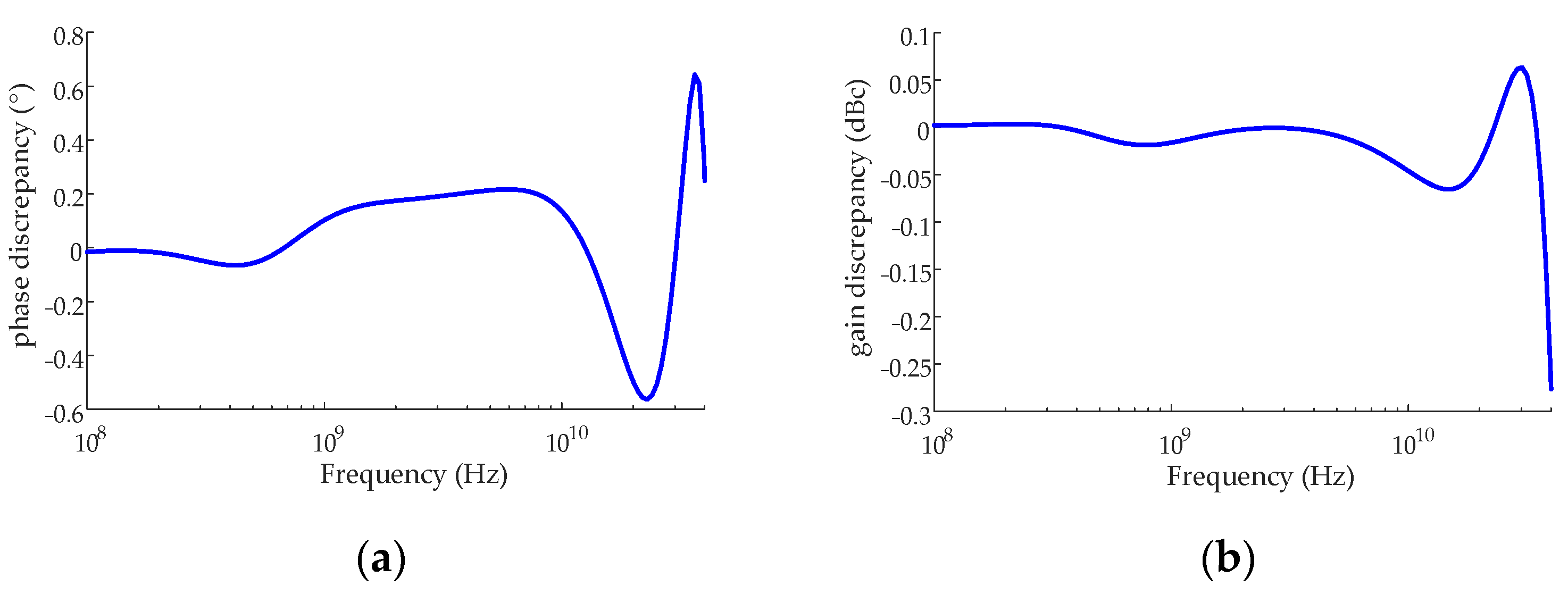
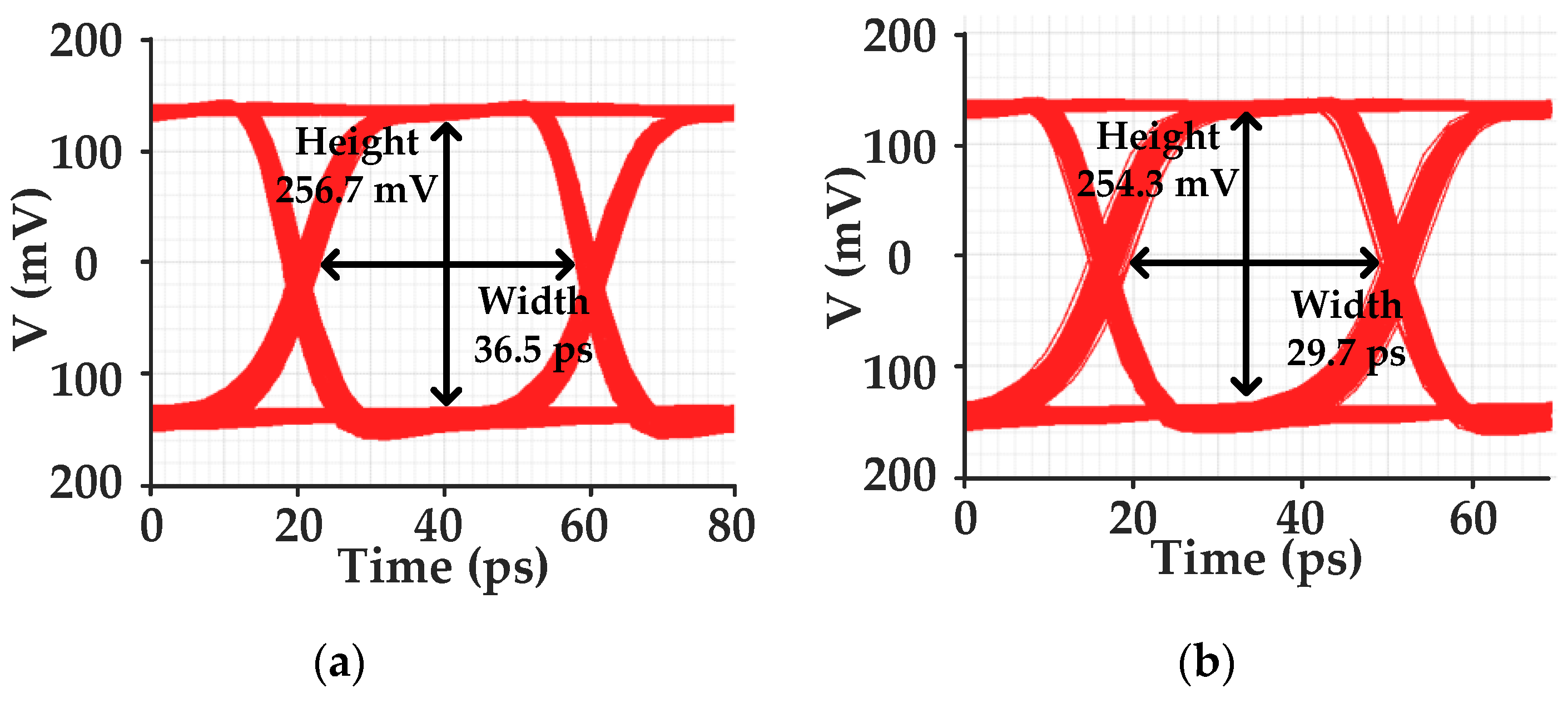
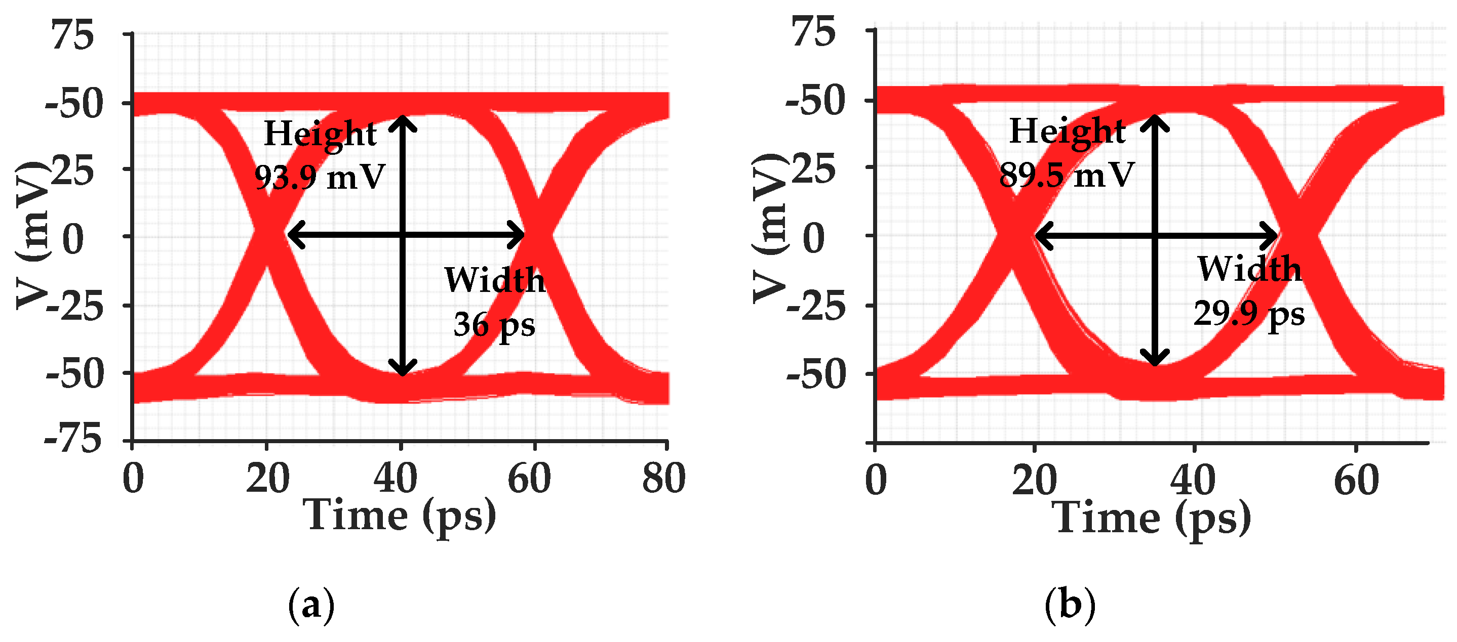
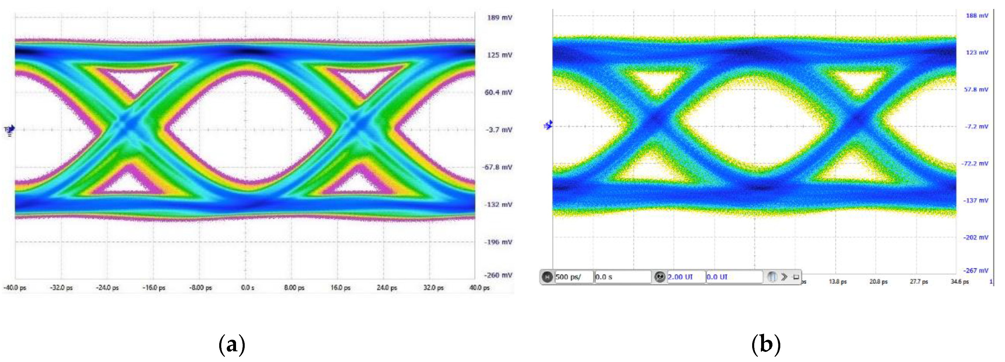
4. Measurement Results, Analysis, and Discussion

Figure 18 shows a chip microphotograph of the four-lane optical receiver. The optical receiver was fabricated via GlobalFoundries 0.13 μm SiGe BiCMOS (GlobalFoundries, Santa Clara, CA, USA) technology, and the one-lane area is about 0.54 mm2. Meanwhile, one lane consumes 84.97 mW in the low-power mode and 123.75 mW in the high-power mode, both with a 3.3 V supply voltage.
In order to explore the eye diagram performance of the optical receiver, an INOPOTICALS Bit Analyzer BA8042 (INOPOTICALS, Taiwan) was used to produce 27 − 1 pseudo-random bit sequence (PRBS7) data patterns to the optical receiver, while a Keysight digital signal analyzer DSAZ254A (Keysight, Santa Rosa, CA, USA) was used to measure the output eye diagram. The Bit Analyzer BA8042 was also implemented to measure the BER performance with a given PRBS7 input signal.
The measured eye diagrams with a 300 μApp input signal (for PRBS7) are presented in Figure 19a,b, where the receiver works in high-power mode. The measured results of the eye diagrams in Figure 19a,b are given in Table 1. The eye heights with input signals at 25 Gb/s and 28.9 Gb/s are 154.2 mV and 114.8 mV, respectively. The eye diagram at 25 Gb/s has a much larger eye height than the eye diagram at 28.9 Gb/s. The crossing of the eye diagram become larger with higher data rates, as shown in Table 1. Additionally, the measured BER of the optical receiver with a 200 μApp input signal varying from 25 Gb/s to 28.9 Gb/s (for PRBS7) is 10−12 when the receiver works in both high-power mode and low-power mode.
A performance summary of the presented optical receiver and comparison with previous works is given in Table 2. The measured minimum input current of the proposed receiver is 110 μApp with minimized noise of the DCOC loop and the input TIA stage. The minimum input current is kept low by the improved stability of the input TIA. Meanwhile, the one-lane area of the receiver is reduced to 0.54 mm2, almost half that of prior works in SiGe BiCMOS technology, with parasitics utilization in the DCOC loop and capacitive emitter degeneration in the VGA stage. The one-lane area of the receiver is even smaller than the arts inadvanced CMOS technology. We simplified the power supply solution with a single power supply. Compared with previous works, this work provides a wider range of data rates and transimpedance, which suits different communication environments.

5. Conclusions

An area-efficient programmable 4 × 25-to-28.9 Gb/s optical receiver was designed and implemented herein. With the optimization mentioned above in terms of area reduction, the one-lane area is only 0.54 mm2. Meanwhile, the measured BER is 10−12 with a 110 μA minimum input current due to the improved noise optimization and programmability of the optical receiver. With a 3.3 V power supply, the power dissipation varies from 84.97 mW to 123.7 mW in low-power and high-power modes, respectively. Consequently, the proposed optical receiver shows good performance in terms of area efficiency and programmability when compared to previous designs.

Author Contributions

Conceptualization, H.X. and J.L.; methodology, H.X. and J.L.; visualization, H.X.; validation, H.X. and J.L.; formal analysis, H.X.; resources, F.Y.; writing—original draft preparation, H.X.; writing—review and editing, H.X., J.L., Z.W., M.Z., J.M. and F.Y.; project administration, J.L. and F.Y.; funding acquisition, J.L. and F.Y. All authors have read and agreed to the published version of the manuscript.

Funding

This work was supported in part by the National Natural Science Foundation of China under Grant 61604128 and the Fundamental Research Funds for the Central Universities under Grant 2017QN81002.

Acknowledgments

The authors would like to thank the Institute of Aerospace Electronics Engineering of Zhejiang University for providing the research platform and technical support.

Conflicts of Interest

The authors declare no conflict of interest. The information of author has been changed.

References

  1. Greshishchev, Y.; Schvan, P. A 60 dB gain 55 dB dynamic range 10 Gb/s broadband SiGe HBT limiting amplifier. In Proceedings of the 1999 IEEE International Solid-State Circuits Conference, San Francisco, CA, USA, 17 February 1999; pp. 382–383. [Google Scholar]
  2. Shibasaki, T.; Tsunoda, Y.; Oku, H.; Ide, S.; Mori, T.; Koyanagi, Y. 4 × 25 Gb/s retimer ICs for optical links in 0.13 μm SiGe BiCMOS. In Proceedings of the 2015 IEEE International Solid-State Circuits Conference, San Francisco, CA, USA, 22–26 February 2015; pp. 1–3. [Google Scholar]
  3. Knochenhauer, C.; Hauptmann, S.; Scheytt, J.C.; Ellinger, F. A Jitter-Optimized Differential 40-Gbit/s Transimpedance Amplifier in SiGe BiCMOS. IEEE Trans. Microw. Theory Tech. 2010, 58, 2538–2548. [Google Scholar] [CrossRef]
  4. Moeneclaey, B.; Verbrugghe, J.; Blache, F.; Goix, B.; Lanteri, D.; Duval, B.; Achouche, M.; Bauwelinck, J.; Yin, X. A 40-Gb/s Transimpedance Amplifier for Optical Links. IEEE Photonics Technol. Lett. 2015, 27, 1375–1378. [Google Scholar] [CrossRef]
  5. Schild, A.; Rein, H.; Mullrich, J.; Altenhain, L.; Blank, J.; Schrodinger, K. High-gain SiGe transimpedance amplifier array for a 12 × 10 Gb/s parallel optical-fiber link. IEEE J. Solid-State Circuits 2003, 38, 4–12. [Google Scholar] [CrossRef]
  6. Park, S.M. Four-channel SiGe transimpedance amplifier array for parallel optical interconnects. In Proceedings of the 2004 IEEE International Symposium on Circuits and Systems (ISCAS), Vancouver, BC, Canada, 23–26 May 2004. [Google Scholar]
  7. Park, S.M.; Toumazou, C.; Papavassiliou, C. A high-speed four-channel integrated optical receiver array using SiGe HBT technology. In Proceedings of the 2000 IEEE International Symposium on Circuits and Systems (ISCAS), Geneva, Switzerland, 28–31 May 2000; pp. 433–436. [Google Scholar]
  8. Weiner, J.S.; Leven, A.; Houtsma, V.; Baeyens, Y.; Chen, Y.; Paschke, P.; Yang, Y.; Frackoviak, J.; Sung, W.; Tate, A.; et al. SiGe differential transimpedance amplifier with 50-GHz bandwidth. IEEE J. Solid-State Circuits 2003, 38, 1512–1517. [Google Scholar] [CrossRef]
  9. Li, D.; Zhang, Z.; Xie, Y.; Liu, M.; Yang, Q.; Geng, L. A 25 Gb/s low-noise optical receiver in 0.13 μm SiGe BiCMOS. In Proceedings of the 2016 IEEE International Conference on Electronics, Circuits and Systems (ICECS), Monte Carlo, Monaco, 11–14 December 2016; pp. 576–579. [Google Scholar]
  10. Kalogerakis, G.; Moran, T.; Nguyen, T.; Denoyer, G. A quad 25 Gb/s 270 mW TIA in 0.13 Mm BiCMOS with <0.15 dB crosstalk penalty. In Proceedings of the 2013 IEEE International Solid-State Circuits Conference Digest of Technical Papers, San Francisco, CA, USA, 17–21 February 2013; pp. 116–117. [Google Scholar]
  11. Proesel, J.; Schow, C.; Rylyakov, A. 25 Gb/s 3.6 pJ/b and 15 Gb/s 1.37 pJ/b VCSEL-based optical links in 90 nm CMOS. In Proceedings of the 2012 IEEE International Solid-State Circuits Conference, San Francisco, CA, USA, 19–23 February 2012; pp. 418–420. [Google Scholar]
  12. Kokolov, A.A.; Konkin, D.A.; Koryakovtsev, A.S.; Sheyerman, F.I.; Babak, L.I. Microwave Photonic ICs for 25 Gb/s Optical Link Based on SiGe BiCMOS Technology. Symmetry 2019, 11, 1453. [Google Scholar] [CrossRef] [Green Version]
  13. Shahramian, S.; Dehlaghi, B.; Liang, J.; Bespalko, R.; Dunwell, D.; Bailey, J.; Wang, B.; Sharif-Bakhtiar, A.; O’Farrell, M.; Tang, K.; et al. 30.5 A 1.41pJ/b 56Gb/s PAM-4 Wireline Receiver Employing Enhanced Pattern Utilization CDR and Genetic Adaptation Algorithms in 7nm CMOS. In Proceedings of the 2019 IEEE International Solid- State Circuits Conference, San Francisco, CA, USA, 17–21 February 2019; pp. 482–484. [Google Scholar]
  14. Mathew, M.; Hart, B.L.; Hayatleh, K. Design of a low-current shunt-feedback transimpedance amplifier with inherent loop-stability. Analog Integr. Circuits Sign. Proces. 2019, 99, 539–545. [Google Scholar] [CrossRef]
  15. Li, C.; Palermo, S. A Low-Power 26-GHz Transformer-Based Regulated Cascode SiGe BiCMOS Transimpedance Amplifier. IEEE J. Solid-State Circuits 2013, 48, 1264–1275. [Google Scholar] [CrossRef]
  16. Säckinger, E. Broadband Circuits for Optical Fiber Communication, 1st ed.; Agere Systems: Allentown, PA, USA, 2002; p. 119. [Google Scholar]
  17. Xuan, Z.; Ding, R.; Liu, Y.; Baehr-Jones, T.; Hochberg, M.; Aflatouni, F. A Low-Power Hybrid-Integrated 40-Gb/s Optical Receiver in Silicon. IEEE Trans. Microwave Theory Tech. 2018, 66, 589–595. [Google Scholar] [CrossRef]
  18. Alexander, S.B. Optical Communication Receiver Design, 1st ed.; The International Society for Optical Engineering: Bellingham, WA, USA, 1997; pp. 173–182. [Google Scholar]
  19. Takemoto, T.; Matsuoka, Y.; Yamashita, H.; Lee, Y.; Akita, F.; Arimoto, H.; Kokubo, M.; Ido, T. A 50.6-Gb/s 7.8-mW/Gb/s −7.4-dBm sensitivity optical receiver based on 0.18-µm SiGe BiCMOS technology. In Proceedings of the 2016 IEEE Symposium on VLSI Circuits (VLSI-Circuits), Honolulu, HI, USA, 15–17 June 2016; pp. 1–2. [Google Scholar]
  20. Sedighi, B.; Scheytt, J.C. Low-Power SiGe BiCMOS Transimpedance Amplifier for 25-GBaud Optical Links. IEEE Trans. Circuits Syst. Express Briefs 2012, 59, 461–465. [Google Scholar] [CrossRef]
  21. Razavi, B. Design of Integrated Circuits for Optical Communications, 2nd ed.; John Wiley & Sons: Hoboken, NJ, USA, 2012; p. 24. [Google Scholar]
  22. Li, D.; Minoia, G.; Repossi, M.; Baldi, D.; Temporiti, E.; Mazzanti, A.; Svelto, F. A low-noise design technique for high-speed CMOS optical receivers. IEEE J. Solid-State Circuits 2014, 49, 1437–1447. [Google Scholar] [CrossRef]
  23. Säckinger, E. Analysis and Design of Transimpedance Amplifiers for Optical Receivers, 1st ed.; John Wiley & Sons: Hoboken, NJ, USA, 2018; pp. 191–197. [Google Scholar]
  24. El-Diwany, M.H.; Roulston, D.J.; Chamberlain, S.G. Design of low-noise bipolar transimpedance preamplifiers for optical receiver. In IEE Proceedings G - Electronic Circuits and Systems; IET: London, UK, 1981; Volume 128, pp. 299–306. [Google Scholar] [CrossRef]
  25. Gray, P.R.; Hurst, P.J.; Lewis, S.H.; Meyer, R.G. Analysis and Design of Analog Integrated Circuits, 5th ed.; John Wiley & Sons: Hoboken, NJ, USA, 2001. [Google Scholar]
  26. Palmisano, G.; Pennisi, S. CMOS single-input differential-output amplifier cells. In IEE Proceedings-Circuits, Devices and Systems; IET: London, UK, 2003; Volume 150, pp. 194–198. [Google Scholar] [CrossRef]
  27. Kumar, T.B.; Ma, K.; Yeo, K.S. A 4 GHz 60 dB variable gain amplifier with tunable DC offset cancellation in 65 nm CMOS. IEEE Microw. Wirel. Compon. Lett. 2014, 25, 37–39. [Google Scholar] [CrossRef]
  28. Zheng, Y.; Yan, J.; Xu, Y.P. A CMOS VGA With DC Offset Cancellation for Direct-Conversion Receivers. IEEE Trans. Circuits Syst. Regul. Pap. 2009, 56, 103–113. [Google Scholar] [CrossRef]
  29. Takemoto, T.; Yuki, F.; Yamashita, H.; Lee, Y.; Saito, T.; Tsuji, S.; Nishimura, S. A Compact 4 × 25-Gb/s 3.0 mW/Gb/s CMOS-Based Optical Receiver for Board-to-Board Interconnects. J. Light. Technol. 2010, 28, 3343–3350. [Google Scholar] [CrossRef]
Figure 1. A block diagram of the optical receiver.
Electronics 09 01032 g001
Figure 2. Schematic of the input transimpedance amplifier (TIA) stage.
Electronics 09 01032 g002
Figure 3. The simplified small-signal equivalent circuit of the input TIA.
Electronics 09 01032 g003
Figure 4. The noise optimization results of the input TIA.
Electronics 09 01032 g004
Figure 5. The simulated relationship between the damping factor and RE.
Electronics 09 01032 g005
Figure 6. The simulated frequency response of the input TIA.
Electronics 09 01032 g006
Figure 7. The single-ended–differential amplifier (STD) stage block diagram.
Electronics 09 01032 g007
Figure 8. The simulated optical receiver discrepancy. (a) phase discrepancy; (b) gain discrepancy.
Electronics 09 01032 g008
Figure 9. A schematic of the variable-gain amplifier.
Electronics 09 01032 g009
Figure 10. The simulated frequency response of the variable-gain amplifier (VGA).
Electronics 09 01032 g010
Figure 11. A schematic of the output stage.
Electronics 09 01032 g011
Figure 12. Simulated eye diagrams of the receiver in high-power mode. (a) 25 Gb/s; (b) 28.9 Gb/s.
Electronics 09 01032 g012
Figure 13. Simulated eye diagrams of the receiver in low-power mode. (a) 25 Gb/s; (b) 28.9 Gb/s.
Electronics 09 01032 g013
Figure 14. A schematic of the DC offset cancellation (DCOC) circuit.
Electronics 09 01032 g014
Figure 15. The simulated voltage variation of the total parasitic capacitance.
Electronics 09 01032 g015
Figure 16. The simulated process and temperature variation of the total parasitic capacitance.
Electronics 09 01032 g016
Figure 17. Simulated input-referred noise current introduced by the sink currents.
Electronics 09 01032 g017
Figure 18. The microphotograph of the four-lane optical receiver.
Electronics 09 01032 g018
Figure 19. Measured eye diagrams of the optical receiver. (a) 25 Gb/s; (b) 28.9 Gb/s.
Electronics 09 01032 g019
Table 1. Measured results of the eye diagrams.
25 Gb/s28.9 Gb/s
Eye height (mV)154.2114.8
Eye width (UI)0.650.65
Eye one level (mV)126.7116.8
Eye zero level (mV)−129.0−119.5
Crossing (%)51.251.8
Table 2. A comparison of the performance with that in previously published works for one lane.
ReferenceThis Work[10][11][12][29]
Data rate (Gb/s)25–28.9
(4 ch)
25 (4 ch)252525 (4 ch)
Technology0.13 μm SiGe
BiCMOS
0.13 μm SiGe BiCMOS90 nm CMOS0.25 μm SiGe BiCMOS65 nm CMOS
Transimpedance
(dBΩ)
62.8–77.5 *7678.362.969.8
Minimum input current (μApp)11089219N/A285
Power supply (V)3.33.31.23.3/2.51.8/1.0
DC power (mW)84.97/123.7 **67.544.416074
Area (mm2)0.54 ***1.23***0.811.240.4 ***
* Simulated result. ** In low-power mode or high-power mode. *** One-lane area.

