Article

Ultra-Compact Reconfigurable Band Reject UWB MIMO Antenna with Four Radiators

by
Muhammad Saeed Khan
1,†,
Adnan Iftikhar
1,
Raed M. Shubair
2,3,
Antonio-Daniele Capobianco
4,
Sajid Mehmood Asif
5,
Benjamin D. Braaten
6 and
Dimitris E. Anagnostou
7,*
1
Department Electrical and Computer Engineering, COMSATS University Islamabad, Islamabad 45550, Pakistan
2
Research Laboratory of Electronics, Massachusetts Institute of Technology (MIT), Cambridge, MA 02139, USA
3
Department of Electrical and Computer Engineering, New York University, Abu Dhabi 129188, UAE
4
Department of Information Engineering, University of Padova, Via Gradenigo 6/b, 35131 Padova, Italy
5
Electronic and Electrical Engineering, The University of Sheffield, Sheffield S1 4ET, UK
6
Department of Electrical and Computer Engineering, North Dakota State University, Fargo, ND 58102, USA
7
Department of Electrical Engineering, Heriot-Watt University, Edinburgh EH14 4AS, UK
*
Author to whom correspondence should be addressed.
These authors contributed equally to this work.
Electronics 2020, 9(4), 584; https://doi.org/10.3390/electronics9040584
Submission received: 19 February 2020 / Revised: 20 March 2020 / Accepted: 23 March 2020 / Published: 30 March 2020
(This article belongs to the Special Issue Reconfigurable Antennas)

Abstract

:
A compact reconfigurable UWB MIMO antenna with four radiators that accomplish on-demand band rejection from 4.9 to 6.3 GHz is presented. An LC stub is connected to the ground plane by activating the PIN diode for each radiator. Two radiators are placed perpendicular to each other to exploit the polarization diversity on a compact 25 × 50 mm 2 FR4 laminate. Two additional radiators are then fixed obliquely on the same laminate (without increasing size) in angular configuration at ±45 perpendicular to the first two planar radiators still exploiting polarization diversity. The design is validated by prototyping and comparing the results with the simulated ones. On demand band rejection through the use of PIN diodes, wide impedance matching (2–12 GHz), high isolation amongst the radiators, compactness achieved by angular placement of the radiators, low gain variation over the entire bandwidth, band rejection control achieved by adjusting the gap between stub and ground plane, and low TARC values makes the proposed design very suitable for commercial handheld devices (i.e., Huawei E5785 and Netgear 815S housings). The proposed configuration of the UWB MIMO radiators has been investigated first time as per authors’ knowledge.

1. Introduction

For the present and future wireless technologies, Wireless Personal Area Networks (WPANs), Ultra-wideband (UWB), and Multiple Input Multiple Output (MIMO) antennas are fundamental and indispensable transducers. These transducers enhance MIMO system performance using antenna diversity techniques, such as spatial diversity, pattern diversity, or polarization diversity. Nonetheless, unwanted interference from Wireless Local Area Networks (WLAN), i.e., IEEE 802.11 (5.8 GHz), may cause malfunctioning or weak precision in any UWB MIMO transceiver for the UWB application such as sensor data collection, precision locating, or tracking applications [1,2,3,4,5]. Therefore, MIMO antenna designers and researchers have proposed band-reject UWB MIMO antennas to mitigate WLAN interference [6,7,8,9,10].
The use of integrated elements in the feed line can result in multiple band notch characteristics in a UWB antenna, as reported in [6]. The etching of slots in the radiator can also notch dual band in a UWB MIMO antenna [7]. Similarly, introduction of slits in an antenna size of 36 × 36 mm 2 can be used to achieve band notch functionality [8]. In addition, inclusion of stubs in the ground plane can notch a specific band over a UWB spectrum, but this technique results in an overall antenna size of 40 × 68 mm 2 , as reported in [9]. Further, the incorporation of λ /2 open stubs on the antenna having ground plane size of 55 × 86.5 mm 2 successfully achieved a notched band; however, the use of large reflectors restrict further size reduction of the antenna reported in [10]. Likewise, the work presented in [11,12,13] highlights the use of stubs for WLAN band rejection along with the exploitation of polarization diversity for isolation enhancement amongst the elements. Loading of radiator or ground plane with metamaterials can also notch a WLAN band. In this regard, the authors of [14] implemented an Electromagnetic bandgap (EBG) structure for band rejection and a band stop filter for improving coupling. Huang et al. [15] proposed Complementary Split Rings Resonator (CSRR) slots and open stubs near the feedline to achieve band notch functionality. Polarization diversity in the design was attained by vertical placement of the designed antennas [15]. Moreover, defected ground plane in circular monopoles was used to notch 4.6 GHz band, and periodic EBG structures with large number of vias were placed between 4 × 4 MIMO antennas to achieve isolation of more than 17 dB [16]. Similarly, a planar placement of 4 × 4 UWB MIMO antenna having isolation of more than 17 dB was presented in [17]. A four element UWB MIMO antenna with a complex band stop design for the WLAN band resulted in an overall footprint of 39.8 × 50 mm 2 [18], whereas a similar placement of four element UWB antenna having modified ground plane with slots had an overall size of 45 × 45 mm 2 [18]. It can be seen from the aforementioned discussion that researchers have successfully addressed different techniques to notch a single band [8,9,10] or multiple bands [6,7] in UWB MIMO antennas. However, these techniques permanently reject a specific band and thus provide inflexibility in the antenna design to un-notch that specific band. Moreover, most of the antenna designs presented in the literature deliver band rejection in a two elements UWB antenna system.
Conversely, on demand rejection using active switches such as PIN diodes, RF microelectromechanical system (MEMS) switches, and optical switches have also been proposed in the literature [19,20,21,22,23,24]. However, the demonstrations of reconfiguration mechanism/on-demand band rejection has only been performed on a single or at most of two elements antenna system [22]. Therefore, overall system performance of a four-element UWB MIMO antenna having on demand band rejection capabilities cannot be accurately estimated by exploring two element UWB MIMO designs. Besides, a major portion of the literature is focused on the right angled placement of the MIMO antenna elements, which occupies a major portion of the device housing. The right angle placement of UWB MIMO antenna elements occupies extra space and can therefore be unfit for modern 4G LTE WiFi hotspots such as Huawei E5785 and Netgear 815S. Therefore, the objective of this work is twofold: (a) introduce an efficient method of utilizing UWB spectrum by proposing on-demand band rejection through the use of PIN diode;s and (b) present a novel design of a four-element UWB MIMO antenna system which makes use of two slanted radiators placed at an angle of ±45 ; this leads to the capability of on demand band rejection and space saving of device housing.
In this paper, an ultra-compact frequency reconfigurable UWB MIMO antenna is presented. All four radiators are capable of rejecting the WLAN signals on demand by activating the PIN diodes. PIN diodes connect the λ g /4 stub to the ground plane to draw most of the current on the stub. Two radiators are placed on the planar substrate and two radiators are placed angularly at ±45 perpendicular to the planar laminate, as shown in Figure 1. The overall size in the planar configuration is only 25 × 50 mm 2 and specific angular placement of the radiators provide liberty to the designer to use housing height to adjust the radiators. In addition, adding reconfigurability in the proposed design makes it valuable for most of the UWB MIMO applications. The proposed method to reduce the overall size of the UWB MIMO antenna, to the best of authors’ knowledge, has never been investigated before. The use of disconnected ground planes provides fabrication simplicity and mitigate coupling issues in such a closely packed configuration. On the other hand, the incorporation of decoupling structures may replace separate ground planes requirement but at the cost of increased hardware complexity and fabrication challenges [23,24].

2. Design Procedure

The design procedure is started by optimizing the single element of the proposed UWB MIMO antenna for the complete 2–12 GHz frequency range. Multiple techniques have been integrated to achieve the final optimum design which includes impedance transformer with a transmission line for lower band matching (3–5 GHz), tapered section at the input of radiator for matching around 7 GHz and corner truncation of the rectangular patch for the higher band (10–12 GHz). On the bottom side of the radiator, a stub is connected with the partial ground plane to reject the WLAN band. Later, to achieve the reconfigurability of the WLAN band, the stub is connected or disconnected through PIN diodes. When the PIN diode is turned on, the length of the stub acts an inductor, while the gap between the stub and ground plane act as a capacitor, resulting in a LC band-stop filter. The length of the stub is calculated using L s = λ g 4 = c 4 f o ϵ r , where f o ≈ 5 GHz, and ϵ r is the relative permittivity of the substrate. Next, a second element (identical to first element) is placed on the same laminate at a distance of 6.15 mm and rotated by 90 . Due to small spacing, the impedance matching is affected: to improve the input impedance, the second element is then modified by inserting a U-shaped slot. The length and width of U-slot are optimized using L u = λ g 4 = c 4 f o ϵ r and W u = λ g 8 = c 8 f o ϵ r , where f o ≈ 3.65 GHz, and ϵ r is the relative permittivity of the substrate. The comparison of reflection co-efficient with and without U-slot is shown in Figure 2.
As can be seen in Figure 2, the reflection co-efficient of second element is improved when inserting the U-slot. It can be observed that Radiators 1 and 2 are almost identical, the only modification in Radiator 2 being the U-shaped slot. All other parameters of radiators, ground plane, and stubs are exactly same as those for Radiator 1. Now, to add more elements in the design, without increasing further the dimensions of the laminate while keeping low the mutual coupling, two additional radiators are placed perpendicularly to the substrate and slanted in angular configuration at ±45 . The specific angle was chosen after several numerical iterations to have low mutual coupling and polarization diversity between Radiators 3 and 4. In the proposed design, the height of the design is 22 mm. This allows utilizing the height of the housing, which increases from 20 to 80 mm according to the application and design (i.e., Huawei E5785 and Netgear 815S housings). Radiator 3 is identical to Radiator 1 and Radiator 4 is identical to Radiator 2. The final layout of the proposed UWB MIMO antenna system is shown in Figure 1. All EM simulations and design optimization were carried out in ANSYS HFSS.

3. Results and Discussion

3.1. S Parameters

To validate the performance of the proposed antenna, a prototype of the design reported in Figure 1 was fabricated on a 1.6 mm thick FR4 substrate with a relative permittivity of 4.5 and a loss tangent of 0.02. The fabricated prototype is shown in Figure 3. Surface mount voltage controlled PIN diodes were used to connect the stub to the ground plane and control voltage (+V = 0.7 V) was applied on the conducting surface with RF chokes. ANSYS HFSS was used to model the PIN diodes using lumped elements in the simulation and, during measurement, DC biased signal was used to control the ON and OFF state of the PIN diodes.
The reflection coefficient and mutual coupling for ‘ON’ (i.e., all four diodes biased, and the stubs physically connected with the ground) and ‘OFF’ (i.e., all four diodes unbiased, and the stubs physically disconnected from the ground) states were measured using an Agilent N5242A PNA-X network analyzer. These results are shown in Figure 4, Figure 5, Figure 6 and Figure 7. Figure 4a,b shows the comparison of simulated and measured reflection coefficient of Elements 1 and 2 and Elements 3 and 4, respectively, when diodes are OFF. The measured reflection coefficient is better than −10 dB on all ports over the entire band and a good agreement can be seen. The mutual coupling amongst elements is less than −17 dB over the whole band. The simulated and measured mutual couplings are plotted in Figure 5a,b, respectively. Similarly, when diodes are turned ON, measured results regarding reflection coefficient and mutual coupling are plotted in Figure 6 and Figure 7. A strong band rejection was observed from 4.9 to 6.3 GHz.

3.2. Radiation Pattern and Peak Gain

The radiation patterns at three different frequencies (3.5, 5.8, and 9.8 GHz) for ON and OFF state were measured in the anechoic chamber in the principle x-z and y-z planes, and compared with the simulated patterns. During the measurements, all ports were terminated with a 50- Ω matched load except the Port 1. Only slight variations in the patterns were observed outside the rejected band during the ON and OFF state of diodes. Patterns at lower frequencies for both ON and OFF state are fairly dumbbell-shaped in the y-z plane and omnidirectional in the x-z plane, as shown in Figure 8a,b; a good agreement with simulated patterns was observed. At 5.8 GHz, when diodes are turned ON, the antenna radiates with very low intensity, which is evident in Figure 8c,d, while the antenna radiates with high intensity when diodes are turned OFF. At higher frequencies (9.8 GHz), as shown in Figure 8e,f, patterns are still omnidirectional in the x-z plane and slightly deviate from dumbbell-shaped. The discrepancy from simulated results is more evident, due to fabrication tolerances, soldering effects, cable, and connector losses and not ideal PIN diodes and RF chokes.
To check the gain variation, the peak gain over the entire bandwidth was measured for Port 1, as plotted in Figure 9 along with the simulated one for both ON and OFF state. It is evident in Figure 9 that gain lowers to −4 dBi in the rejected band, showing that radiation intensity is very low in this band when diode is turned ON, while the gain rises up to 3.8 dB when diodes are turned OFF. The peak gain variation is less than 3.5 dBi in the entire band while diode is turned OFF.

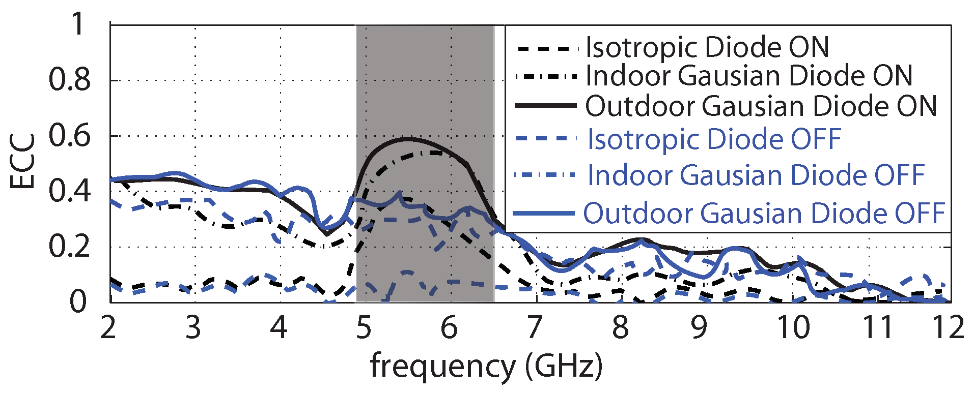
3.3. Diversity Analysis

In MIMO systems, the multipath effects can be mitigated, if two or more elements have different patterns in a particular plane. In the proposed design, Radiators 1 and 2 are placed perpendicular, so they have different patterns in the respective planes. The x-z patterns of Radiator 1 are almost identical to the y-z patterns of Radiator 2. Similarly, Radiators 3 and 4 have pattern diversity, as shown in Figure 10 by plotting 3D radiation patterns at 4 GHz. It can be seen that null is located at 45 when Port 3 is excited and −45 when Port 4 is excited. This behavior can also be visualized by plotting the 2-D radiation patterns of Radiators 3 and 4 in the y-z plane, as shown in Figure 11. It is evident that the simulated and measured patterns of Radiators 3 and 4 are un-correlated and almost orthogonal. In fact, Radiator 3 has a maximum radiation at −45 and 135 , while Radiator 4 has null in those directions. Similarly, Radiator 4 has a maximum radiation at 45 and −135 , while Radiator 3 has null in those directions.
The un-correlated (orthogonal) radiation patterns, giving rise to diversity which is exploited in MIMO technology, are beneficial in a rich multipath environment. To check the performance of the proposed antenna in a complex scenario, envelope correlation coefficient (ECC) was calculated from the far-field radiation patterns. For different environments, such as indoor and outdoor, the parameters calculated in [25] are used in Equation (1) and numerically calculated values of ECC are plotted in Figure 12 for both ON and OFF state. The computed values from far-field radiation patterns are less than 0.43 for all cases. For uniform scattering environments, the values are less than 0.15.
ρ e = 0 2 π 0 π X P R . E θ 1 . E θ 2 . P θ + E φ 1 . E φ 2 . P φ d Ω 2 0 2 π 0 π X P R . E θ 1 . E θ 1 . P θ + E φ 1 . E φ 1 . P φ d Ω × 0 2 π 0 π X P R . E θ 2 . E θ 2 . P θ + E φ 2 . E φ 2 . P φ d Ω
In MIMO systems, when multiple antennas are actively involved in transmission or reception, they change the efficiency and overall operating bandwidth. Therefore, total active reflection coefficient (TARC) should be lower than 0 dB, which incorporates overall combined effect of all antenna in a MIMO system and is determined by Equation (2). TARC is plotted in Figure 13 for both ON and OFF states and is less than −9 dB over the entire band.
T A R C = S 11 + S 12 + S 13 + S 14 2 + S 21 + S 22 + S 23 + S 24 2 + S 31 + S 32 + S 33 + S 34 2 + S 41 + S 42 + S 43 + S 44 2 4

3.4. Parametric Analysis on Bandwidth Control

One of the main advantages of the proposed design is that the rejected frequency region can be controlled by changing the gap (g) between ground plane and stub. To verify this, the gap was varied from 0.25 to 1.5 mm and results are plotted in Figure 14. The variation in the gap changes the capacitance between ground plane and stub, resulting in the change of rejected bandwidth. When the gap is 0.25 mm, the rejected band is from 5.25 to 6.25 GHz, and it keeps on increasing while gap is increased. The maximum bandwidth of the rejected band can be obtained around 2.6 GHz (3.7–6.3 GHz), when the gap is 1.5 mm.
To further investigate the effect of the stub on the antenna, the surface currents are plotted in Figure 15 for both ON and OFF states at 5.8 GHz. It is evident in Figure 15a that stub is not affected when the diode is turned OFF as very little current is coupled on it, while turning the diode ON, high currents flow on the stub (Figure 15b), thus rejecting the band.

3.5. Comparison With Previous Work Done

In Table 1, the proposed antenna is compared with the most representative UWB MIMO antennas existing in the literature. This list in not complete but offers a fair insight on the current work. Some of the existing antennas are compact but do not provide the band notch design; some compact designs provide the band notch design, but bandwidth cannot be controlled. In short, the proposed antenna has improved performance, when compared to all components of other antennas.

4. Conclusions

An ultra-compact reconfigurable four-port UWB MIMO antenna is designed and validated after the numerical optimization. PIN diodes are used to reconfigure the WLAN band (4.9–6.3 GHz) by applying a controlled voltage. PIN diodes connect the LC stubs to the ground plane, providing an extra path to current to travel and reject the WLAN band. The rejected bandwidth can be controlled by changing the gap between stub and ground plane. Planar and slanted placement of the radiators allow achieving high compactness. A prototype was fabricated on FR4 laminate; reflection coefficients, mutual coupling, radiation patterns, peak gain, ECC, and TARC were compared with the simulated results showing good agreement. Compactness and reconfigurability of the proposed UWB MIMO antenna make it a very strong candidate for commercial handheld devices.

Author Contributions

M.S.K. provided the idea and performed complete simulations. A.I. performed design, fabrication, and measurements. S.M.A. post processed simulation and measured results. A.-D.C., R.M.S., B.D.B., and D.E.A. assisted in overall paper management, idea development, and manuscript writing. All authors have read and agreed to the published version of the manuscript.

Funding

This work was supported in part by the EU H2020 Marie Skłodowska-Curie Individual Fellowship through ViSionRF under Grant 840854 and funded by COMSATS University, Islamabad under COMSATS Research Grant Program (Project#16-63/CGRP/CUI/ISB/18/847).

Conflicts of Interest

The authors declare no conflict of interest.

References

  1. Kaiser, T.; Zheng, F.; Dimitrov, E. An Overview of Ultra-Wide-Band Systems with MIMO. Proc. IEEE 2009, 97, 285–312. [Google Scholar] [CrossRef]
  2. Vaughan, R.G.; Andersen, J.B. Antenna diversity in mobile communications. IEEE Trans. Veh. Tech. 1978, 36, 149–172. [Google Scholar] [CrossRef]
  3. Xu, H.-X.; Wang, G.-M.; Qi, M.-Q. A miniaturized triple-band metamaterial antenna with radiation pattern selectivity and polarization diversity. Prog. Electromagn. Res. 2013, 137, 275–292. [Google Scholar] [CrossRef] [Green Version]
  4. First Report and Order, Revision of Part 15 of the Commissions Rule Regarding Ultra Wideband Transmission Systems; Federal Communication Commission: Washington, DC, USA, 2002; pp. 2–48.
  5. Anagnostou, D.E.; Chryssomallis, M.T.; Braaten, B.D.; Ebel, J.L.; Sepulveda, N. Reconfigurable UWB antenna with RF-MEMS for on demand WLAN Rejection. IEEE Trans. Antennas Propag. 2014, 62, 602–608. [Google Scholar] [CrossRef]
  6. Zhu, F.; Gao, S.; Ho, A.T.; Abd-Alhameed, R.A.; See, C.H.; Brown, T.W.C.; Li, J.; Wei, G.; Xu, J. Multiple band-notched UWB antenna with band rejected elements integrated in the feed line. IEEE Trans. Antennas Propag. 2014, 61, 3952–3960. [Google Scholar] [CrossRef]
  7. Li, J.-F.; Chu, Q.-X.; Li, Z.-H.; Xia, X.-X. Compact dual band-notched UWB MIMO antenna with high isolation. IEEE Trans. Antennas Propag. 2012, 61, 4759–4766. [Google Scholar] [CrossRef]
  8. Zhao, H.; Zhang, F.; Zhang, X.; Wang, C. A compact band-notched ultra-wideband Spatial diversity antenna. Prog. Electromagn. Res. 2014, 51, 19–26. [Google Scholar] [CrossRef] [Green Version]
  9. Najam, A.; Duroc, Y.; Tedjni, S. UWB-MIMO antenna with novel stub structure. Prog. Electromagn. Res. 2011, 19, 245–257. [Google Scholar] [CrossRef] [Green Version]
  10. Lee, J.-M.; Kim, K.-B.; Ryu, H.-K.; Woo, J.-M. A compact ultrawideband MIMO antenna with WLAN band-rejected operation for mobile devices. IEEE Antennas Wirel. Propag. Lett. 2012, 11, 990–993. [Google Scholar]
  11. Yoon, H.K.; Yoon, Y.J.; Kim, H.; Lee, C.H. Flexible ultrawideband polarization diversity antenna with band-notch function. IET Microw. Antennas Propag. 2011, 5, 1463–1470. [Google Scholar] [CrossRef]
  12. Gao, P.; He, S.; Wei, X.; Xu, Z.; Wang, N.; Zheng, Y. Compact printed UWB diversity slot antenna with 5.5 GHz band-notched characteristics. IEEE Antennas Wirel. Propag. Lett. 2014, 13, 376–379. [Google Scholar] [CrossRef]
  13. Chacko, B.P.; Augustin, G.; Denidni, T.A. Uniplanar slot antenna for ultrawideband polarization-diversity applications. IEEE Antennas Wirel. Propag. Lett. 2013, 12, 88–91. [Google Scholar] [CrossRef]
  14. Kiem, N.K.; Phuong, H.N.B.; Chein, D.N. Design of compact 4×4 UWB-MIMO antenna with WLAN band rejection. Int. J. Antennas Propag. 2014, 2014, 1–11. [Google Scholar] [CrossRef]
  15. Huang, H.; Liu, Y.; Zhang, S.S.; Gong, S.X. Compact polarization diversity ultrawideband MIMO antenna with triple band-notched characteristics. Microw. Opt. Technol. Lett. 2015, 57, 946–953. [Google Scholar] [CrossRef]
  16. Wu, W.; Yuan, B.; Wu, A. A quad-element UWB-MIMO antenna with band-notch and reduced mutual coupling based on EBG structures. Int. J. Antennas Propag. 2018, 2018, 1–10. [Google Scholar] [CrossRef] [Green Version]
  17. Khan, M.S.; Capobianco, A.-D.; Asif, S.; Iftikhar, A.; Braaten, B.D. A 4 element compact ultra-wideband MIMO antenna array. In Proceedings of the 2015 IEEE International Symposium on Antennas and Propagation, Vancouver, BC, Canada, 19–25 July 2015. [Google Scholar]
  18. Khan, M.S.; Iftikhar, A.; Asif, S.; Capobianco, A.-D.; Braaten, B.D. A Compact four Elements UWB MIMO antenna with on-demand WLAN rejection. Microw. Opt. Tech. Lett. 2016, 58, 270–276. [Google Scholar] [CrossRef]
  19. Jung, C.W.; Lee, M.; Li, G.P.; De Flaviis, F. Reconfigurable scanbeam single-arm spiral antenna integrated with RF-MEMS switches. IEEE Trans. Antennas Propag. 2006, 54, 455–463. [Google Scholar] [CrossRef]
  20. Khan, M.S.; Asif, S.; Capobianco, A.D.; Ijaz, B.; Anagnostou, D.E.; Braaten, B.D. Frequency reconfigurable self-adapting conformal array for changing wedge- and cylindrical-shaped surfaces. IET Microw. Antennas Propag. 2016, 10, 897–901. [Google Scholar] [CrossRef]
  21. Shelley, S.; Costantine, J.; Christodoulou, C.G.; Anagnostou, D.E.; Lyke, J.C. FPGA-controlled switch-reconfigured antenna. IEEE Antennas Wirel. Propag. Lett. 2010, 9, 355–358. [Google Scholar] [CrossRef]
  22. Zhao, X.; Riaz, S.; Geng, S. A reconfigurable MIMO/UWB MIMO antenna for cognitive radio applications. IEEE Access 2019, 7, 46739–46747. [Google Scholar] [CrossRef]
  23. Fatima, A.; Saleem, R.; Shabbir, T.; Rehman, S.-U.; Bilal, M.; Shafique, M.F. A compact quad-element UWB-MIMO antenna system with parasitic decoupling mechanism. Appl. Sci. 2019, 9, 2371. [Google Scholar]
  24. Kumar, P.; Urooj, S.; Alrowais, F. Design of quad-port MIMO/Diversity antenna with tripple-band elimination characteristics for super wideband applications. Sensors 2020, 20, 624. [Google Scholar] [CrossRef] [PubMed] [Green Version]
  25. Knudsen, M.B.; Pedersen, G.F. Spherical outdoor to indoor power spectrum model at the mobile terminal. IEEE J. Sel. Areas Commun. 2002, 20, 1156–1168. [Google Scholar] [CrossRef]
  26. Anitha, R.; Vinesh, P.V.; Prakash, K.C.; Mohanan, P.; Vasudevan, K. A compact quad element slotted ground wideband antenna for MIMO applications. IEEE Trans. Antennas Propag. 2016, 64, 4550–4553. [Google Scholar] [CrossRef]
Figure 1. Perspective view of the proposed UWB MIMO antenna (dimensions in mm): L = 50, W = 25, g = 0.5, L p = 10, W p = 15, W p 1 = 5, W u = 5, L u = 10, L c = 1.5, W c = 2, W c 1 = 2.25, L t = 6, L t 1 = 3.82, W g = 13.5, L g = 7, L s = 7.25, H = 22, and S p = 6.15. Radiators 1 and 2 are identical in shape and size to radiators 3 and 4, respectively.
Electronics 09 00584 g001
Figure 2. Comparison of the simulated reflection coefficient of Radiators 1 and 2 with and without U-slot. A mismatch is observed at lower frequencies, when U-slot is not inserted in one of the radiators.
Electronics 09 00584 g002
Figure 3. Fabricated prototype with dimensions shown in Figure 1: (a) back side view with PIN diodes and RF chokes; (b) perspective view; and (c) antenna mounted in chamber for pattern measurements.
Electronics 09 00584 g003
Figure 4. Simulated and measured reflection coefficient below −10 dB, when diodes are turned OFF: (a) comparison of simulated and measured reflection coefficients at Ports 1 and 2; and (b) comparison of simulated and measured reflection coefficients at Ports 3 and 4.
Electronics 09 00584 g004
Figure 5. Simulated and measured mutual couplings less than −17 dB amongst all ports, when diodes are turned OFF: (a) simulated; and (b) measured only.
Electronics 09 00584 g005
Figure 6. Simulated and measured reflection coefficient below −10 dB except the rejected band, where values reach −1 dB almost at all input ports, when diodes are turned ON (a) comparison of simulated and measured reflection coefficients at Ports 1 and 2; and (b) comparison of simulated and measured reflection coefficients at Ports 3 and 4.
Electronics 09 00584 g006
Figure 7. Simulated and measured mutual couplings less than −17 dB amongst all ports, when diodes are turned ON: (a) simulated; and (b) measured only.
Electronics 09 00584 g007
Figure 8. Simulated and measured radiation patterns in the principle planes, when diodes are turned OFF (red color) and turned ON (black color): (a) x-z plane at 3.5 GHz; (b) y-z plane at 3.5 GHz; (c) x-z plane at 5.8 GHz; (d) y-z plane at 5.8 GHz; (e) x-z plane at 9.8 GHz; and (f) y-z plane at 9.8 GHz. The patterns are nearly omni-directional in the x-z plane, suitable for UWB MIMO systems.
Electronics 09 00584 g008
Figure 9. Simulated and measured peak gain over the entire band, when diodes are turned ON and OFF; the gain varies from 2.0 to 5.5 dBi except the rejected band during ON state, where gain drops down to −4 dBi.
Electronics 09 00584 g009
Figure 10. Simulated 3D radiation patterns at 4 GHz showing the pattern diversity for Ports 3 and 4: (a) only Port 3 is excited; and (b) only Port 4 is excited.
Electronics 09 00584 g010
Figure 11. Simulated and measured radiation patterns of Radiators 3 and 4 in the y-z plane at 4 GHz plane showing strong un-correlation at some angles and almost orthogonal, useful for diversity applications.
Electronics 09 00584 g011
Figure 12. Computed envelope correlation coefficients between Radiators 3 and 4 from far-field radiation pattern for isotropic (uniform), indoor and outdoor environments. The XPR values used for indoor and outdoor environment are 5 and 1 dB, respectively. The ECC values are less than 0.43 in all cases.
Electronics 09 00584 g012
Figure 13. Simulated and measured TARC for both ON and OFF state calculated from S-parameters. TARC is lower than −9 dB over the entire band.
Electronics 09 00584 g013
Figure 14. Effects of the gap variation between ground plane and stub on reflection coefficients. While the values are changed from 0.25 to 1.50 mm, the rejected bandwidth can be controlled from 1 to 2.6 GHz.
Electronics 09 00584 g014
Figure 15. Surface current distribution for OFF and ON state: (a) exciting Port 1 at 5.8 GHz, while diode is OFF; and (b) exciting Port 1 only at 5.8 GHz, while diode is turned ON. The plot illustrates that stub only has current on it in the rejected band, when diode is turned ON.
Electronics 09 00584 g015
Table 1. Performance comparison with previous literature.
Published LiteratureTotal PCB Size
without Height (mm 2 )
Bandwidth
(GHz)
Notch Band
(GHz)
|S 11 | at Notch
(or Notch Quality)
Bandwidth Control/Complex
or Simple Structure/
Recon-Figurable
Mutual Coupling
(dB)
Gain Var-(dBi)/
Notch Band Gain
(dBi)
ECC Using
Far-Field Patterns
[26]
Anitha et al.
45 × 452.2–6.28NoN.AN.A≤−14<4/
N.A
<0.25
(uniform)
[17]
Asif et al.
50 × 39.82.5–12NoN.AN.A≤−17<N.A/
N.A
N.A
[18]
Asif et al.
50 × 39.82.7–124.8–6.2−2 dBNot presented/
complex design
structure used
to obtain
notch/Yes
≤−17<4/
−3.8
N. A
[14]
Keim et al.
60 × 602.73–10.685.36–6.04−1.8 dBNot presented /
complex EBG
structure/No
<−15<5/
−3.7
N.A
[16]
Wenjing et al.
60 × 603.0–16.24.0–5.2−1.4 dBNot presented /
complex EBG
structure with
vias/No
<−17.5<6/
−1
<0.3
(uniform)
Proposed
antenna
25 × 502–124.9–6.3−1 dBYes/simple
LC stub/
Yes
<−17<3.5/
−4
<0.15 (uniform)
<0.43 (indoor)
<0.43 (outdoor)

