Abstract
A new circuit structure of LLC converter is studied and implemented to achieve wide zero-voltage switching range and wide voltage operation such as consumer power units without power factor correction and long hold up time demand, battery chargers, photovoltaic converters and renewable power electronic converters. The dc converter with the different secondary winding turns is adopted and investigated to achieve the wide input voltage operation (50–400 V). To meet wide voltage operation, the full bridge and half bridge dc/dc converters with different secondary turns can be selected in the presented circuit to have three different voltage gains. According to input voltage range, the variable frequency scheme is employed to have the variable voltage gain to overcome the wide input voltage operation. Therefore, the wide soft switching load variation and wide voltage operation range are achieved in the presented resonant circuit. The prototype circuit is built and tested and the experiments are demonstrated to investigate the circuit performance.
1. Introduction
Power electronics are more and more important for the energy conversion systems such as renewable power conversion, electric vehicle systems, traction vehicles, light rail vehicles, dc nano- or micro-grid systems, battery-based storage systems, personal computer power units and industry power units. Power semiconductors such as insulated gate bipolar transistors (IGBTs), Metal-Oxide-Semiconductor Field-Effect Transistor (MOSFET), Gallium Nitride (GaN) FET and Silicon Carbide (SiC) devices are widely used power switches in power electronic circuits. However, IGBT devices have low switching frequency problem. GaN and SiC devices have the advantages of low switching loss and high frequency operation. However, the cost of GaN and SiC is much more expensive than the IGBT and MOSFET devices. Compared to IGBT, GaN and SiC devices, MOSFET elements have low cost and medium frequency operation for modern power converters. Pulse-width modulation (PWM) power electronic circuits have been widely studied and developed in power electronics to lessen reduce global warming and air pollution problems. The dc-dc or dc-ac power converters are the most attractive interface circuits between the photovoltaic (PV) cells (or fuel cells) and the utility dc or ac voltage. However, the output voltage of PV cells, fuel cells and dc wind turbine power generators is not constant and related to solar intensity or wind speed. Conventional duty cycle control converters [1,2,3,4] and frequency control converters [5,6,7] cannot be operated well under wide voltage variation condition due to the limit voltage gain of power converters. Multi-stage dc converters with parallel or series structure [8,9,10,11] have been researched to overcome wide voltage variation problem and used for renewable energy conversion and battery charger applications. However, the disadvantages of multi stage dc-dc converters have low reliability and more active and passive power components. Two full bridge circuits structure was presented in [12] to overcome limit voltage range problem of conventional resonant converters. However, sixteen power semiconductors are used in this circuit structure. The conventional LLC converter with two sets of secondary windings was studied in [13] to have wide hold-up time operation for PC power units. The main drawbacks of this circuit structure are four secondary windings and large copper losses. The resonant converter with interleaved duty cycle control was achieved in [14] to overcome wide voltage variation problem and achieve low current ripple input. However, the circuit topology is still the multi stage converter.
The new resonant converter with voltage doubler configuration and two sets of secondary windings is presented in this paper to accomplish soft switching operation and overcome wide voltage input variation (Vin = 50–400 V). According to the input voltage range, the present LLC converter can be operated under full bridge resonant structure or half bridge resonant structure with different secondary turns. Therefore, the proposed converter has much wide range of input voltage operation. When Vin = 50–100 V (low voltage region), the full bridge type LLC circuit with more secondary turns is operated to have high voltage gain. If Vin = 100–200 V (medium voltage input region), the full bridge type LLC circuit with fewer secondary turns is adopted to have less dc voltage gain. If Vin = 200–400 V (high voltage input region), the half bridge structure is used to obtain the lowest voltage gain on the presented circuit. With the proposed control strategy, the wide voltage operation (Vin = 50–400 V) is accomplished in the presented circuit structure. Since the proposed resonant circuit is controlled under the variable switching frequency with input inductive impedance operation, the active switches have soft switching turn-on characteristic. The voltage doubler rectification structure can reduce the voltage rating of diodes compared to the center-tapped rectifier topology. Thus, the diode conduction loss can be reduced. The proposed LLC converter has less circuit components compared to the wide voltage resonant converter presented in [8,9,10,11,12,13,14]. Finally, the experimental verifications are provided to demonstrate the performance of the studied LLC resonant circuit.
2. Circuit Configuration and Principles of Operation
The conventional resonant converters with half bridge or full bridge structure are provided in Figure 1. The fundamental root-mean-square (rms) input voltage of full bridge structure is two times of the fundamental rms input voltage of half bridge structure. Therefore, the full bridge resonant converter has more power capability than the half bridge resonant converter. Owing to the center-tapped rectification structure, the diodes D1 and D2 has at least 2Vo voltage stress. The other disadvantage of the center-tapped rectifier is two winding sets are needed on the secondary side of transformer T. For high load current applications, there are more copper losses on the secondary windings.

Figure 1.
Structures of the conventional LLC converters: (a) full bridge LLC structure; (b) half bridge LLC structure.
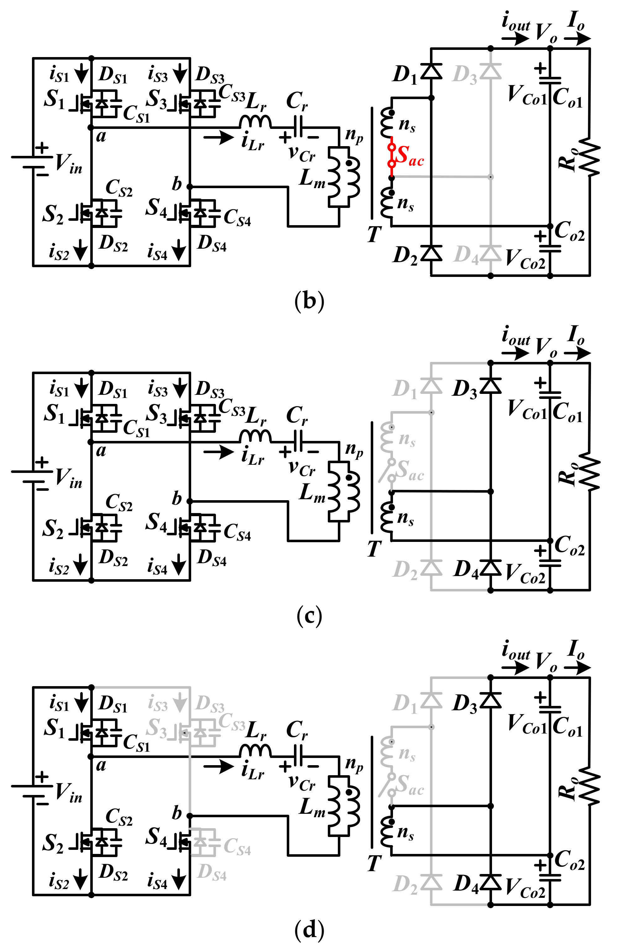
The proposed LLC hybrid converter is provided in Figure 2a to overcome the disadvantage of narrow voltage range in conventional LLC converter. The adopted circuit comprises a full bridge resonant circuit and a voltage double rectifier with variable winding turns to have wide voltage operation capability (50–400 V) and wide soft switching operation. Lr is the series resonant inductance, Lm is the magnetizing inductance and Cr is the series resonant capacitance. According to the switching status of S1–S4, the converter can operate as the full bridge circuit structure (Figure 2b,c) or half bridge circuit structure (Figure 2d). The LLC resonant tank with Cr, Lr and Lm is operated with variable frequency to have inductive input impedance and zero-voltage turn-on switching for all devices S1–S4. The variable secondary turns are controlled by Sac to achieve different voltage gains. Sac is realized with two back-to-back MOSFETs. According to the adopted circuit configuration, the converter has three operation sub-circuits under three different input voltage regions. Figure 2b–d give the equivalent circuits for low, medium and high input voltage conditions respectively. If 50 V < Vin < 100 V (low voltage region Vin,L), then switches S1–S4 are controlled by frequency modulation and Sac is in the on-state. Figure 2b gives the circuit diagram for low input voltage operation. The voltage vab has voltage level Vin or −Vin. The 2ns winding turns and diodes D1 and D2 are connected to output load. The voltage gain under low input voltage region is obtained as Vo/Vin,L = Gac(fsw)(4ns)/np, where Gac(f) is the voltage transfer function of resonant tank. From the conduction states of the power semiconductors, the circuit in Figure 2b has six or four states in one switching period under the fr (series resonant frequency) > or < fsw (switching frequency). If 100 V < Vin < 200 V (medium voltage region Vin,M), Sac turns off and Figure 2c gives the equivalent circuit configuration. It is clear to observe that D2 and D1 are off. The ns winding turns and diodes D3 and D4 are connected to load.

Figure 2.
Proposed converter: (a) circuit diagram; (b) low input voltage region; (c) medium input voltage region; (d) high input voltage region.
The voltage gain in Figure 2c is Vo/Vin,M = Gac(fsw)(2ns)/np. If 200 V < Vin < 400 V (high voltage region Vin,H), the active switches S3 and Sac are turned off and S4 is always in the on-state. Figure 2d illustrates the circuit diagram operated at high voltage region. The leg voltage vab has voltage level Vin or 0. Only ns winding turns and diodes D3 and D4 are connected to load. The voltage gain in Figure 2d is Vo/Vin,H = Gac(fsw)ns/np. From the three voltage gains in previous discussion, it can observe that Vo/Vin,L = Gac(fsw)(4ns)/np = 2Vo/Vin,M = 4Vo/Vin,H. Thus, one can conclude that Vin,H = 2Vin,M = 4Vin,L. Therefore, the proposed LLC converter has the highest voltage gain at low voltage region Vin,L and the lowest voltage gain at high voltage region Vin,H.
2.1. Low Voltage Region (Vin,L: 50–100 V)
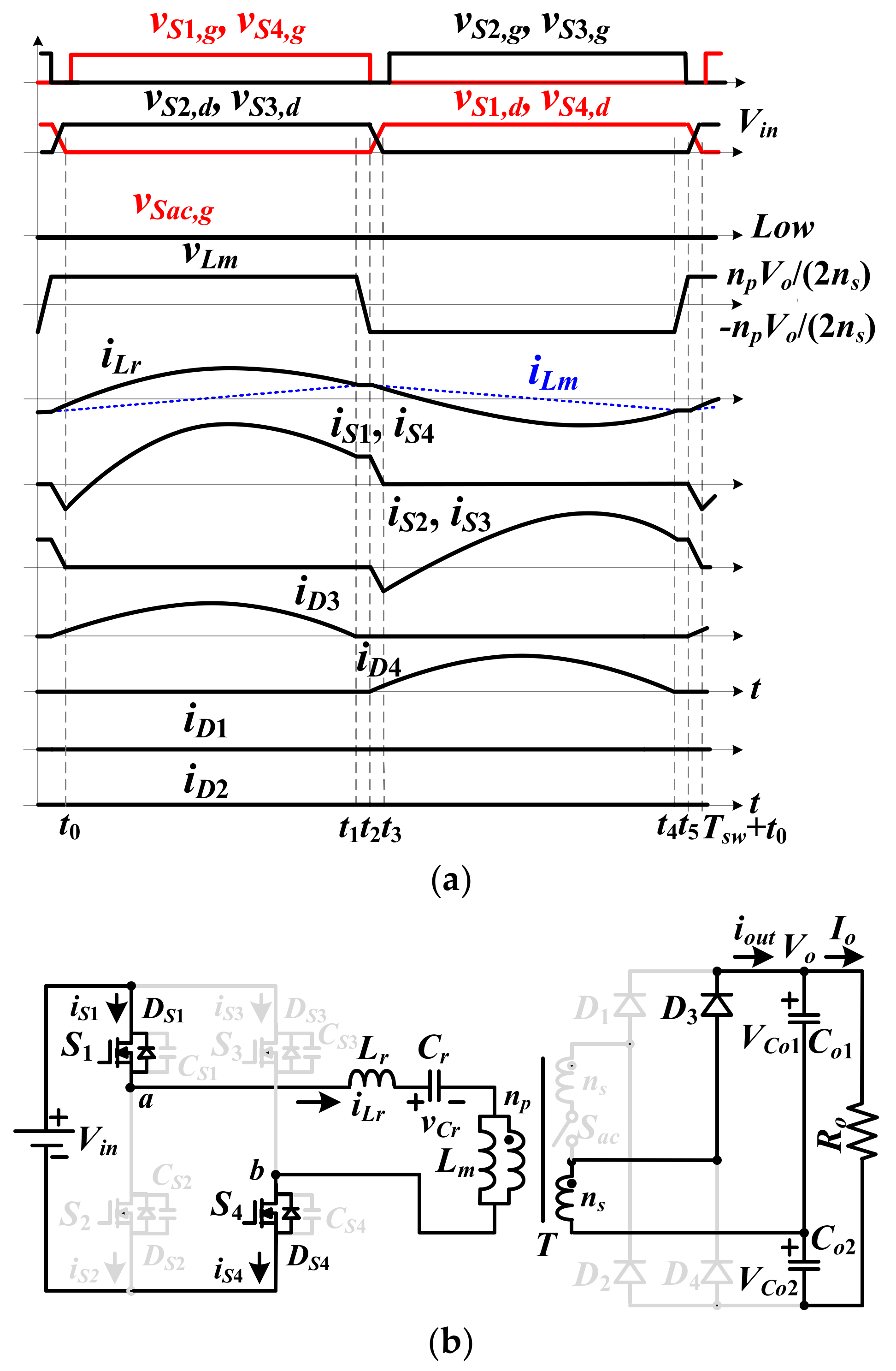
When Sac is in the on-state, the LLC converter has less transformer turns-ratio np/(2ns) and large voltage gain. Under this condition, the rectifier diodes D3 and D4 are always off. The voltage gain of the converter is obtained as Vo/Vin,L = Gac(fsw)(4ns)/np. From the gating signals of S1–S4 and the on/off state of D1 and D2, six equivalent operating states per switching periods are provided in Figure 3.

Figure 3.
LLC converter at low input voltage region: (a) key PWM waveforms; (b) state 1 equivalent circuit; (c) state 2 equivalent circuit; (d) state 3 equivalent circuit; (e) state 4 equivalent circuit; (f) state 5 equivalent circuit; (g) state 6 equivalent circuit.
State 1 [t0–t1]: When t = t0, vCS1 = vCS4 = 0 V. Power devices S4 and S1 turn on at this moment to realize soft switching operation due to iLr(t0) < 0. Since iLr > iLm, D1 conducts in this state. In state 1, vab = Vin,L, vLm = (VCo1np)/(2ns) ≈ (Vonp)/(4ns) and iLm increases. The resonant frequency of the LLC converter in this state is . If fr,1 > or < fsw, then the circuit operation will go to state 2 or 3.
State 2 [t1–t2]: When iD1 = 0 at t1, D1 is turned off with zero-current switching. The resonant frequency in state 2 is . It is obvious that fr,1 > fr,2. The current variation on Lm approximates and the magnetizing current iLm at t2 is .
State 3 [t2–t3]: Power devices S1 and S4 are off at time t2. Since iLr(t2) is positive, vCS3 and vCS2 are decreased. Due to iLm(t2) > iLr(t2), D2 is conducting. To ensure the soft switching turn-on of S3 and S2, the current iLm(t2) must be greater than where Coss = CS1 = … = CS4. The other necessary condition for zero-voltage switching is that the dead time td between S2 and S1 is greater than time interval in state 3. To accomplish this condition, one can obtain .
State 4 [t3–t4]: At time t3, vCS2 = vCS3 = 0 V. At this moment, power devices S3 and S2 are turned on under zero voltage. Owing to iLm(t3) > iLr(t3), D2 conducts. In state 2, vab = −Vin,L, vLm = −(VCo2np)/(2ns) ≈ −(Vonp)/(4ns), iLm decreases and Co1 (Co2) is discharged (charged). If fr,1 > or < fsw, then the circuit operation will go to state 4 or 6.
State 5 [t4–t5]: If fr,1 > fsw, one obtains iD2 equals 0 at t4. Then, D2 turns off. The resonant frequency in state 4 is . The magnetizing current iLm at t5 approximates .
State 6 [t5–Tsw + t0]: S3 and S2 turn off at t5. CS1 and CS4 are discharged owing to iLr(t5) < 0. Since iLr(t5) > iLm(t5), the rectifier diode D1 conducts. To achieve soft switching turn-on of S4 and S1, the magnetizing inductor current iLm at t5 is obtained and expressed as .
2.2. Medium Voltage Region (Vin,M: 100–200 V)
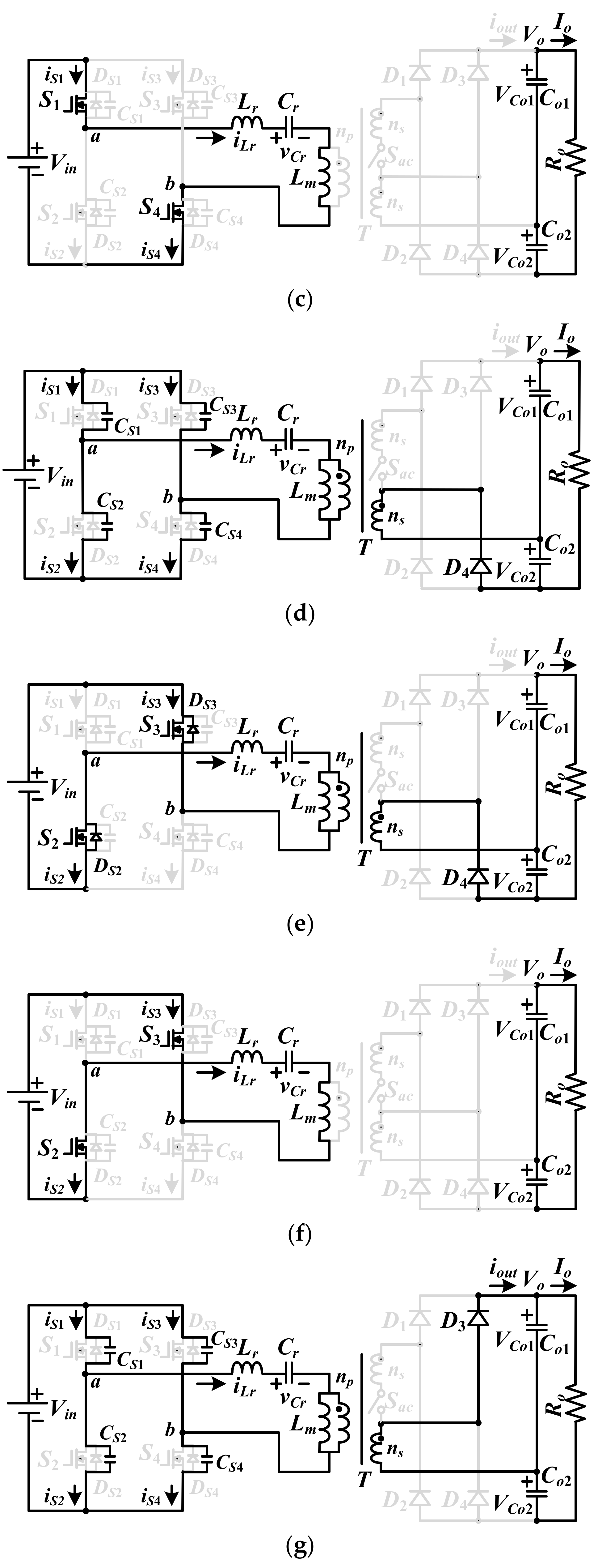
If Vin is in the medium voltage region between 100 V and 200 V, the switch Sac is tuned off. The converter has low transformer turns-ratio np/ns and less voltage gain. The circuit diagram is shown in Figure 2c. The voltage gain at medium voltage operation is equal to Vo/Vin,M = Gac(fsw)(2ns)/np. Figure 4 shows the key PWM waveforms and state circuits for medium voltage operation (100–200 V).

Figure 4.
LLC converter at medium input voltage region: (a) key PWM waveforms; (b) state 1 equivalent circuit; (c) state 2 equivalent circuit; (d) state 3 equivalent circuit; (e) state 4 equivalent circuit; (f) state 5 equivalent circuit; (g) state 6 equivalent circuit.
State 1 [t0–t1]: The drain-to-source voltages of S1 and S4 are decreased and equal to zero at t0. Due to iLr(t0) < 0, the primary-side current iLr flows through the anti-parallel diodes DS4 and DS1. Power devices S4 and S1 turn on at this moment to accomplish soft switching turn-on. Since iLr > iLm, D3 conducts. From Figure 4b, it can obtain that vab = Vin, vLm ≈ (Vonp)/(2ns), iLm increases and the resonant frequency . In this state, Co1 is charged and Co2 is discharged.
State 2 [t1–t2]: If fr,1 > fsw, then iD3 is decreased to zero ampere at time t1 and D3 turns off at zero-current switching. Then, the resonant frequency in state 2 is . The magnetizing current iLm at the end of this state is .
State 3 [t2–t3]: Power devices S4 and S1 are turned off in state 3. The positive primary current iLr(t2) will discharge CS2 and CS3. Owing to iLm(t2) > iLr(t2), D4 on the output-side is conducting. The soft switching turn-on condition of S3 and S2 is . To ensure vCS2 = vCS3 = 0 at t3, the maximum magnetizing inductance Lm,max is obtained as .
State 4 [t3–t4]: The vCS3 and vCS2 are decreased to zero at t3. The primary-side current iLr(t3) is positive and flows through the body diodes DS2 and Ds3. At this moment, power devices S3 and S2 turn on to realize zero-voltage switching. Since iLm(t3) > iLr(t3), D4 conducts. From Figure 4e, it can obtain that vab = −Vin, vLm ≈ −(Vonp)/(2ns) and iLm decreases. The output capacitors Co1 and Co2 are discharged and charged.
State 5 [t4–t5]: iD4 is decreased and equal to zero at t4. Then, D4 turns off. The resonant frequency in state 5 is . The magnetizing current iLm at t5 approximates .
State 6 [t5–Tsw + t0]: Power devices S3 and S2 turn off in this state. iLr(t5) is negative and discharges CS1 and CS4. Since iLr(t5) > iLm(t6), D3 is conducting. The soft switching turn-on condition of S4 and S1 is obtained as .
2.3. High Voltage Region (Vin,H: 200–400 V)
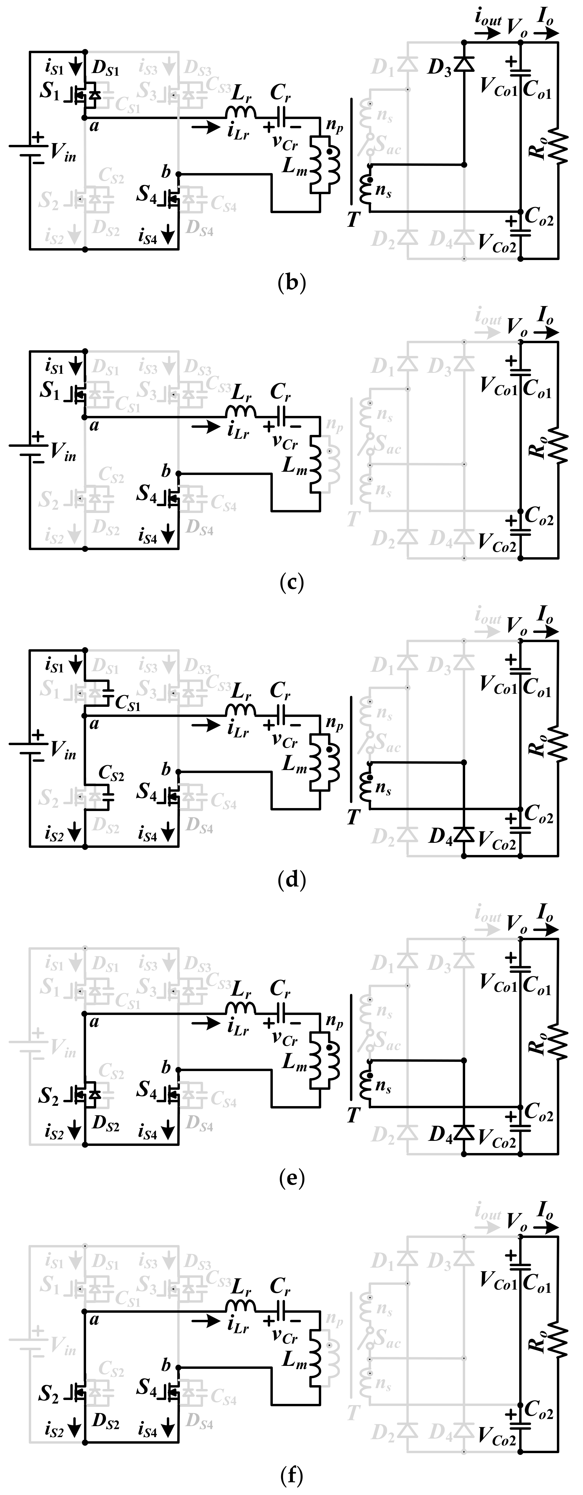
When Vin is increased from 200 V to 400 V, the presented circuit is controlled under high input voltage region. Power devices S3 and Sac turn off and S4 turns on. Only power semiconductors S2 and S1 are controlled with frequency modulation so that the half bridge LLC resonant circuit (S1, S2, S4, Lr, Cr and T) is operated on the input-side. The voltage gain of the converter at high voltage region is Vo/Vin,H = Gac(fsw)ns/np. From the on/off state of D3, D4, S1 and S2, six equivalent operating states per switching periods can be observed in Figure 5 for high input voltage range (200–400 V).


Figure 5.
LLC converter at low high voltage region: (a) key PWM waveforms; (b) state 1 equivalent circuit; (c) state 2 equivalent circuit; (d) state 3 equivalent circuit; (e) state 4 equivalent circuit; (f) state 5 equivalent circuit; (g) state 6 equivalent circuit.
State 1 [t0–t1]: The capacitor voltage vCS1 = 0 at time t0. The primary-side current iLr(t0) is negative so that the body diode DS1 conducts and the leg voltage vab = Vin. Due to iLr > iLm, D3 is forward biased. The inductor voltage vLm ≈ (Vonp)/(2ns). The resonant frequency and Co1 is charged in this state.
State 2 [t1–t2]: If fr,1 > fsw, iD3 = 0 at time t1. Then D3 is turned off at zero-current switching. The resonant frequency in state 2 is expressed as . At time t2, and S1 turns off.
State 3 [t2–t3]: Power device S1 is turned off in this state. The primary current iLr(t2) is positive and discharges CS2. To ensure the soft switching turn-on of S2, the inductor current iLm(t2) must greater than . The other necessary condition for zero-voltage switching is that the dead time td between S2 and S1 is greater than time interval in state 3. To achieve this condition, the magnetizing inductance can obtain .
State 4 [t3–t4]: The drain-to-source voltage vCS2 = 0 at t3. The primary current iLr(t3) > 0 and iLr flows through the body diode DS2. At this moment, S2 turns on to have zero-voltage switching operation. Since iLr(t3) < iLm(t3), D4 is conducting. From Figure 5e, it is clear that vab = 0, vLm ≈ −(Vonp)/(2ns) and iLm decreases.
State 5 [t4–t5]: iD4 is decreased to zero at time t4 and D4 turns off at zero-current switching. The resonant frequency in state 5 is . S2 is turned off at the end of this state and iLm(t5) is expressed as .
State 6 [t5–Tsw + t0]: Owing to iLr(t5) < 0, iLr discharge CS1. The soft switching turn-on of S1 is . The capacitor CS1 is discharged to zero voltage at time t0 + Tsw.
3. Circuit Characteristics and Design Example
The proposed LLC resonant converter is operated by variable frequency control. The square voltage waveform is generated on the leg voltage vab with voltage values ±Vin in Figure 2b,c or Vin and 0 in Figure 2d. The circuit characteristics of the converter are based on the fundamental frequency analysis. Figure 6 gives the equivalent resonant circuit on the input-side. Re,ac is the primary-side resistance of transformer T and vab,rms is the input fundamental voltage. From the leg voltage vab in Figure 2, the fundamental root mean square (rms) voltage vab,rms can be expressed in Equation (1).
Figure 6.
The equivalent resonant circuit on the primary-side.
In low input voltage operation, Sac is always in the on-state. The equivalent turns-ratio of transformer T in Figure 2b is np/(2ns) and the rms value of the magnetizing voltage . In medium and high input voltage ranges (Figure 2c,d), Sac is always in the off-state. The equivalent turns-ratio of transformer T is np/ns. Thus, the rms value of the magnetizing voltage . The primary-side equivalent resistance Re,ac is obtained as in low input voltage operation or in medium and high input voltage operation. From the resonant circuit in Figure 6, the output/input transfer function is expressed in Equation (2).
The output voltage Vo can be expressed in Equations (3)–(5) for low, medium and high input voltage regions.
In the proposed circuit, the electric specifications are Vin = 50–400 V, Vo = 48 V and Po = 500 W. The design resonant frequency fr = 100 kHz. The assumed inductance ratio Lm/Lr is 6. Since the resonant tank is identical for the operation in low, medium and high voltage ranges as shown in Figure 6, the following design procedures are based on the high input voltage condition (Vin,H = 200–400 V). The assume voltage gain of resonant converter is 0.95 at Vin = 400 V case. Thus, the primary-secondary turn np/ns can be calculated as.
np/ns = Gac(fsw)Vin/Vo = 0.95 × 400/48 = 7.916
The transformer T is implemented by using the magnetic core TDK EE-55 with primary turns np = 16 and secondary turns ns = 2. Therefore, the actual voltage gains at 200 V and 400 V input cases are rewritten as.
Gac,max = npVo/nsVin = 1.92
Gac,min = npVo/nsVin = 0.96
According to the winding turns and the load resistor at full load, Re,ac is calculated in Equation (9).
It is assumed the quality factor Rac = 0.1. Then, Lr can be derived in Equation (10).
From the given inductance ratio Lm/Lr = 6, Lm is calculated as Lm = 6 × Lr = 60 μH. The series resonant capacitance Cr is expressed in Equation (11).
The maximum voltage rating of S1–S4 equals Vin,max (= 400 V). The voltage rating of D1–D4 is equal to Vo (= 48 V). Power switches STF40N60M2 (650 V/22 A) are used for S1–S4 and switch IXTP160N075T (75 V/160 A) is used for Sac in the prototype circuit. Power diodes MBR40100PT (100 V/40 A) are adopted in the prototype for the rectifier diodes D1–D4. The selected capacitances Co1 and Co2 are 940 μF with 100 V voltage rating. The control block of a laboratory prototype is shown in Figure 7a. Two Schmitt voltage comparators (comp 1 and comp 2) with reference voltages at 100 V and 200 V are used to select three input voltage regions. The control unit of the converter is using the integrated circuit UCC25600. The logic gates such as AND and OR gates are used to generate the control PWM signals of Sac, S3 and S4. The relationship between the PWM signals of power switches and the input voltage is provided. It can observe that Sac is always ON and S1–S4 are active if 50 V < Vin < 100 V. If 200 V > Vin > 100 V, Sac is always OFF and S1–S4 are active. When Vin > 200 V, Sac and S3 are always OFF, S4 is always ON, and S1 and S2 are active.

Figure 7.
Laboratory prototype: (a) circuit diagram and control block; (b) control signal and input voltage.
4. Experimental Results
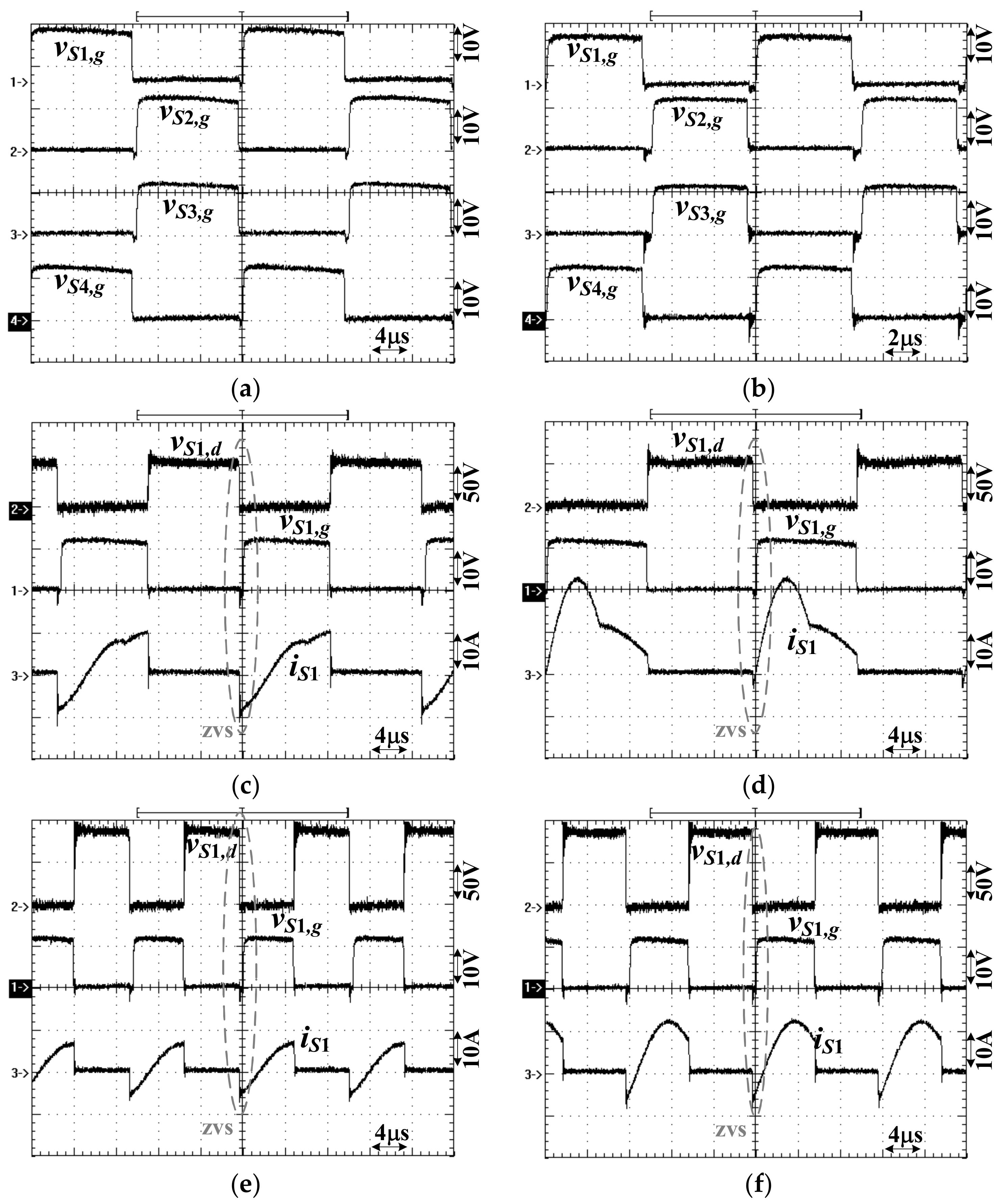
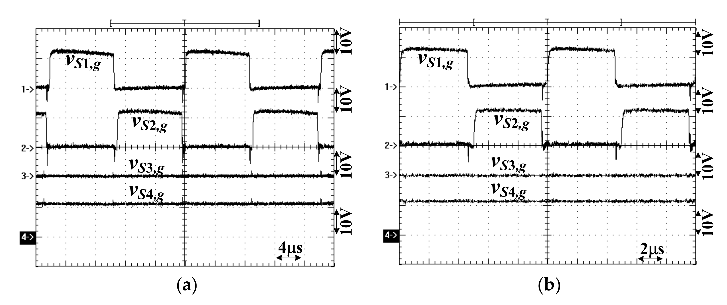
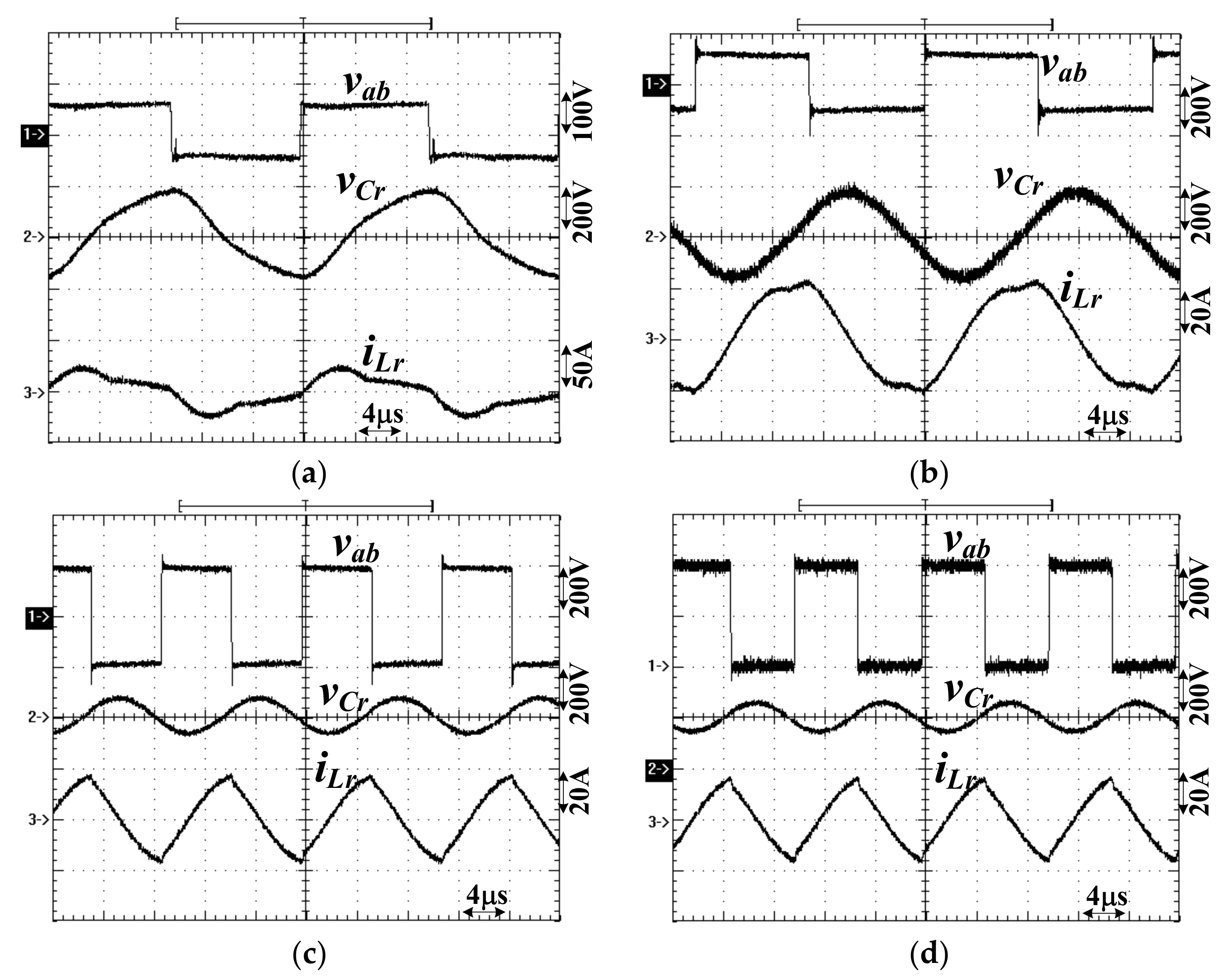
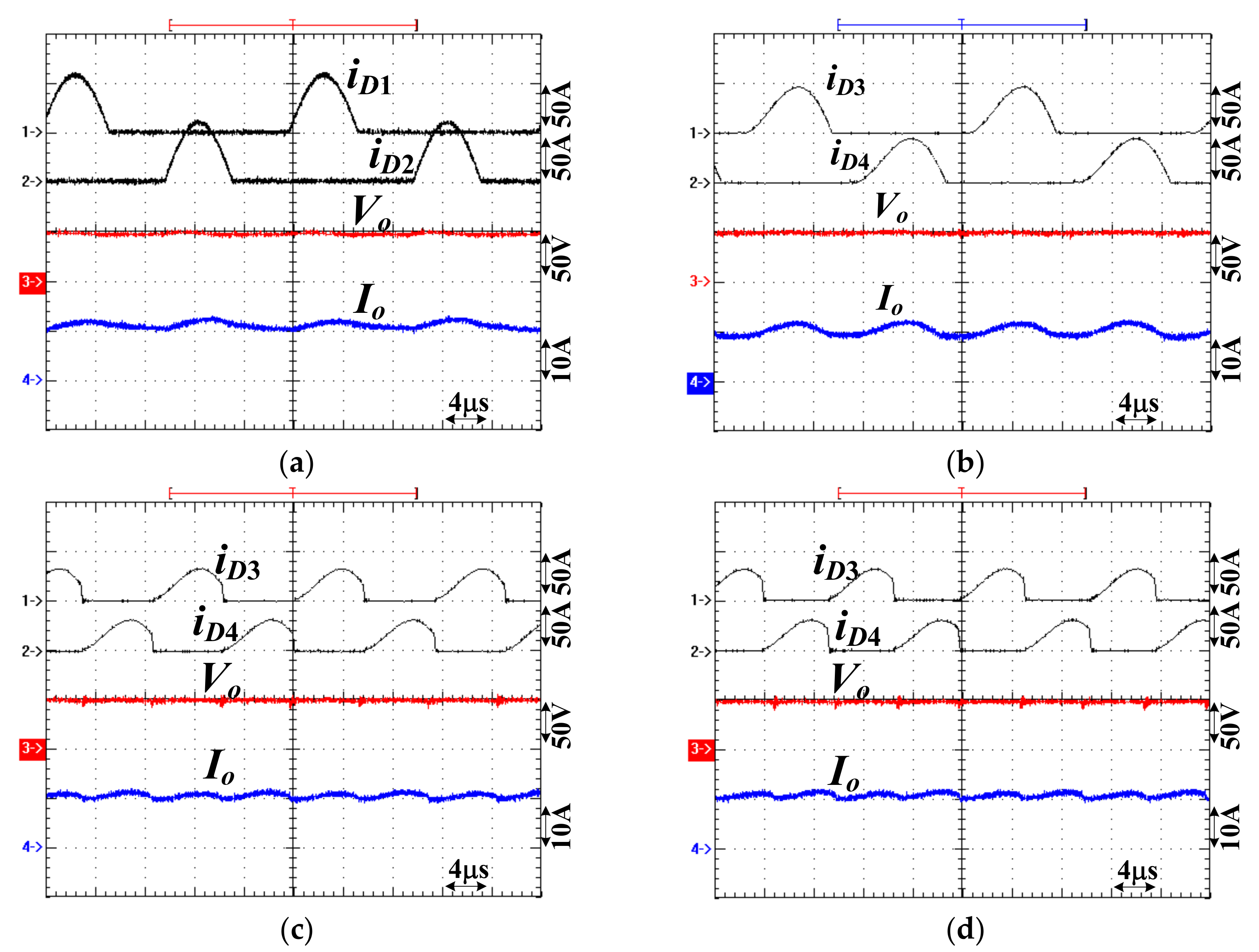
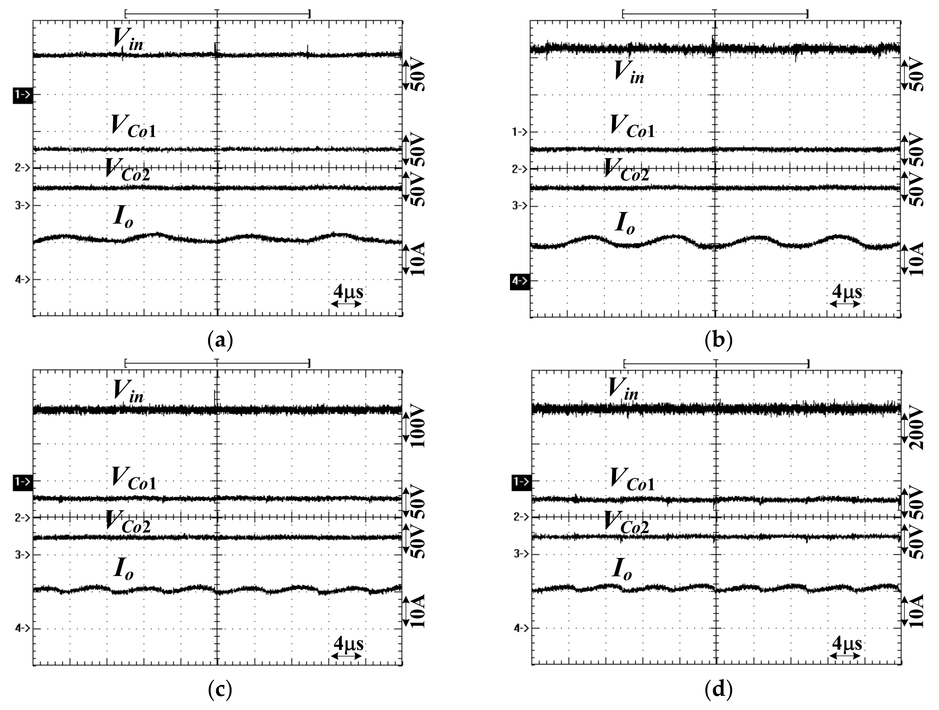
The experimental waveforms are provided to confirm the effectiveness of the presented resonant converter. Figure 8, Figure 9 and Figure 10 gives the experimental results of PWM signals of S1–S4 for low, medium and high input voltage regions, respectively. For low voltage region operation, Sac always turns on, the 2ns secondary turns are connected to load and diodes D3 and D4 are the reverse biased. The gating signals vS1,g–vS4,g under 50 V and 90 V input conditions are provided in Figure 8a,b. The converter operated at Vin = 50 V condition has the low switching frequency compared to 90 V input condition. Figure 8c,d provide the test waveforms of S1 at 20% and 100% output power under 50 V input condition. Similarly, the test waveforms of S1 at 20% and 100% output power under 90 V input condition are provided in Figure 8e,f. One can observe the switch S1 is tuned on at zero voltage switching for both 50 V and 90 V input conditions from 20% output power. Power switches S2–S4 have the similar switching characteristics as switch S1. Thus, the soft switching turn-on of S1–S4 can be achieved under low voltage input region. In the same manner, the measured results of S1–S4 for medium and high voltage input regions are shown in Figure 9 and Figure 10, respectively. For high voltage input region, the half bridge LLC resonant converter is activated and controlled. Thus, S3 and S4 are always turn-off and turn-on as shown in Figure 10a,b, respectively. Figure 11 gives the test waveforms vab, vCr and iLr at Vin = 50 V, 110 V, 190 V and 400 V conditions. In the same manner, the experimental results of the rectifier diode currents, load voltage and load current at Vin = 50 V, 110 V, 190 V and 400 V conditions are shown in Figure 12. For 50 V input case, the studied converter is controlled at low voltage input region and Sac is turned on. The turns-ratio of transformer T is np/2ns. Diodes D3 and D4 are off. Since the studied circuit has much more voltage gain at Vin = 50 V than Vin = 100 V, the circuit operated at Vin = 50 V has less switching frequency. It can observe that D1 and D2 turn off without the reverse recovery current loss shown in Figure 12a. For Vin = 110 V (Figure 12b) and 190 V (Figure 12c) conditions, the circuit is operation in medium input voltage range. Sac is in the off-state and the transformer turns-ratio is np/ns. Diodes D1 and D2 are inactive. The voltage gain of the converter operated at Vin = 110 V is greater than Vin = 190 V condition. Therefore, the switching frequency at 110 V input (Figure 11b is less than 190 V input condition (Figure 11c). Since fsw (switching frequency) at 110 V input is lower than fr (resonant frequency), D3 and D4 are turned off under zero-current switching shown in Figure 12b. For Vin = 400 V input, the resonant converter is operation at high voltage input region. S3 and Sac are always turn-off and switch S4 is always in the on-state. One can observe there is a dc voltage value (Vin/2 = 200 V) on voltage vCr shown in Figure 11d. Owing to fsw > fr at 400 V input, D3 and D4 are turned off with hard switching shown in Figure 12d. The experimental results of Vin, VCo1, VCo2 and Io for different input voltage conditions are provided in Figure 13. It observes that VCo1 and VCo2 are balanced well each other under different input voltage conditions. Figure 14a gives the measured input voltage Vin, the gating voltage vSac,g and output voltage Vo between 50 V (low voltage region)–130 V (medium voltage region) input. When Vin is lower or greater than 100 V, Sac turns on (low input voltage range) or off (medium input voltage range). Figure 14b gives test waveforms of Vin, vS3,g and vS4,g between Vin = 0 V and 250 V. If Vin is lower (or greater) than 200 V, S3 is active (or always turn-off) and S4 is active (or always turn-on). The test PWM signals of S3, S4 and Sac and input voltage Vin shown in Figure 14 are agreed with the theoretical waveforms shown in Figure 7.
Figure 8.
Experimental results of PWM signals for low input voltage region: (a) S1–S4 at 50 V input and 100% power; (b) S1–S4 at 90 V input and 100% power; (c) S1 voltage and current at 50 V input and 20% power; (d) S1 voltage and current at Vin = 50 V input and 100% power; (e) S1 voltage and current at 90 V input and 20% power; (f) S1 voltage and current at 90 V input and 100% power.
Figure 9.
Experimental results of PWM signals for medium input voltage region: (a) S1–S4 at 110 V input and 100% power; (b) S1–S4 at 190 V input and 100% power; (c) S1 voltage and current at 110 V input and 20% power; (d) S1 voltage and current at Vin = 110 V input and 100% power; (e) S1 voltage and current at 190 V input and 20% power; (f) S1 voltage and current at 190 V input and 100% power.

Figure 10.
Experimental results of PWM signals for high input voltage region: (a) S1–S4 at 210 V input and 100% power; (b) S1–S4 at 400 V input and 100% power; (c) S1 voltage and current at 210 V input and 20% power; (d) S1 voltage and current at Vin = 210 V input and 100% power; (e) S1 voltage and current at 400 V input and 20% power; (f) S1 voltage and current at 400 V input and 100% power.
Figure 11.
Measured primary-side voltage and current waveforms at 100% load: (a) 50 V input (low voltage range); (b) 110 V input (medium voltage range); (c) 190 V input (medium voltage range); (d) 400 V input (high voltage range).
Figure 12.
Experimental results of the secondary-side currents and load voltage at 100% load; (a) 50 V input (low voltage range); (b) 110 V input (medium voltage range); (c) 190 V input (medium voltage range); (d) 400 V input (high voltage range).
Figure 13.
Measured results of Vin, VCo1, VCo2 and Io at 100% load: (a) 50 V input (low voltage range); (b) 110 V input (medium voltage range); (c) 190 V input (medium voltage range); (d) 400 V input (high voltage range).
Figure 14.
Measured waveforms: (a) Vin, vSac and Vo; (b) Vin, vS3,g and vS4,g.
5. Conclusions
The hybrid LLC converter with three equivalent sub-circuit topologies is proposed and discussed to realize wide soft switching turn-on and wide voltage input operation. According to the switching status of power devices, the full bridge and half bridge LLC circuit with variable transformer turn-ratio are operated to accomplish wide voltage operation (Vin = 50–400 V). Owing to the LLC circuit tank, power switches have soft switching characteristic at turn-on instant. The presented resonant converter can be applied to dc-dc converters with wide voltage variation capability such as power units in PV power converters, power servers with large hold-up times and battery chargers and dischargers. The experimental results are demonstrated and provided to confirm the effectiveness of the adopted circuit topology.
Author Contributions
B.-R.L. designed and evaluated this project and was also responsible for writing this paper. Y.-C.L. measured the experimental waveforms. All authors have read and agreed to the published version of the manuscript.
Funding
This research is supported by the Ministry of Science and Technology (MOST), Taiwan, under grant number MOST 108-2221-E-224-022-MY2.
Acknowledgments
The authors are grateful to the all the editor and the reviewers for their valuable suggestions to improve this paper.
Conflicts of Interest
The author declares no conflict of interest.
References
- Kim, J.Y.; Kim, H.S.; Baek, J.W.; Jeong, D.K. Analysis of effective three-level neutral point clamped converter system for the bipolar LVDC distribution. Electronics 2019, 8, 691. [Google Scholar] [CrossRef]
- Almalaq, Y.; Matin, M. Three topologies of a non-isolated high gian switched-capacitor step-up cuk converter for renewable energy applications. Electronics 2018, 7, 94. [Google Scholar] [CrossRef]
- Lin, B.R. Phase-shift pwm converter with wide voltage operation capability. Electronics 2020, 9, 47. [Google Scholar] [CrossRef]
- Lin, B.R. Analysis of a dc converter with low primary current loss and balance voltage and current. Electronics 2019, 8, 439. [Google Scholar] [CrossRef]
- Steigerwald, R.L. A comparison of half-bridge resonant converter topologies. IEEE Trans. Power Electron. 1988, 3, 174–182. [Google Scholar] [CrossRef]
- Lin, B.R.; Chu, C.W. Hybrid full-bridge and LLC converter with wide ZVS range and less output inductance. IET Power Electron. 2016, 9, 377–384. [Google Scholar] [CrossRef]
- Lee, J.B.; Kim, J.K.; Baek, J.I.; Kim, J.H.; Moon, G.W. Resonant capacitor on/off control of half-bridge LLC converter for high efficiency server power supply. IEEE Trans. Ind. Electron. 2016, 63, 5410–5415. [Google Scholar] [CrossRef]
- Sun, W.; Xing, Y.; Wu, H.; Ding, J. Modified high-efficiency LLC converters with two split resonant branches for wide input-voltage range applications. IEEE Trans. Power Electron. 2018, 33, 7867–7870. [Google Scholar] [CrossRef]
- Hu, H.; Fang, X.; Chen, F.; Shen, Z.J.; Batarseh, I. A modified high-efficiency LLC converter with two transformers for wide input-voltage range applications. IEEE Trans. Power Electron. 2013, 28, 1946–1960. [Google Scholar] [CrossRef]
- Lu, J.; Kumar, A.; Afridi, K.K. Step-down impedance control network resonant DC-DC converter utilizing an enhanced phase-shift control for wide-input-range operation. IEEE Trans. Ind. Appl. 2018, 54, 4523–4536. [Google Scholar] [CrossRef]
- Jeong, Y.; Kim, J.K.; Lee, J.B.; Moon, G.W. An asymmetric half-bridge resonant converter having a reduced conduction loss for DC/DC power applications with a wide range of low-input voltage. IEEE Trans. Power Electron. 2017, 32, 7795–7804. [Google Scholar] [CrossRef]
- Lin, B.R. Resonant converter with soft switching and wide voltage operation. Energies 2019, 12, 3479. [Google Scholar] [CrossRef]
- Lin, B.R. Series resonant converter with auxiliary winding turns: Analysis, design and implementation. Int. J. Electron. 2018, 105, 836–847. [Google Scholar] [CrossRef]
- Lin, B.R. Resonant converter with wide input voltage range and input current ripple free. IET Proc. Electron. Lett. 2018, 54, 1086–1088. [Google Scholar] [CrossRef]
Publisher’s Note: MDPI stays neutral with regard to jurisdictional claims in published maps and institutional affiliations. |
© 2020 by the authors. Licensee MDPI, Basel, Switzerland. This article is an open access article distributed under the terms and conditions of the Creative Commons Attribution (CC BY) license (http://creativecommons.org/licenses/by/4.0/).