1. Introduction
Given the lack of energy and the climate changes due to increasing fossil fuel consumption over the last few decades, using renewable energies could be a way to help the planet Earth survive in a future energy crisis [
1]. However, in order to utilize the renewable energies, power electronics converters are inevitably essential to produce the required voltage and current for different applications. Among different types of renewable energies, solar energy is more popular as a limitless source of energy, which is spread all over the world. Although the output voltage of photovoltaic (PV) cells are relatively low, applying high step-up DC–DC converters can lead to increasing the voltage level without connecting in series numerous PV panels to enhance the operation of photovoltaic systems, especially in low-power applications [
2].
Research on high step-up converters in recent years has led to the present diverse topologies that are used to resolve existing drawbacks such as high voltage stress of semiconductor devices, reverse-recovery problem of diodes, and intense spike on switches which mostly appear in conventional boost converters by increasing the duty cycle [
3,
4]. Consequently, the topological alteration of the conventional boost converter was proposed by researchers to extend the input-to-output voltage ratio while the circuit operation is enhanced as well. To overcome the drawbacks of boost converters with high efficiency and their simple control scheme, boost converters based on different techniques were proposed by researchers, such as a coupled inductor based boost converter, switched-capacitor based boost converter, cascaded boost converter, and interleaved boost converter [
5]. All introduced converters have some weaknesses and strengths that make them restricted for specific applications. A better performance of a high step-up converter may be obtained if it could be possible to apply different techniques in a converter.
Inserting coupled inductors into the DC–DC converters is an effective method to increase the voltage gain by adjusting the turn ratio between the windings in a topology. Although by increasing the leakage inductance, the reverse-recovery problem of diodes can be reduced effectively due to inserting coupled inductors, the leakage energy induces high voltage spikes across the semiconductor switches. One approach in order to solve this problem is employing a switched-capacitor technique as an active clamp circuit in order to recycle the leakage energy [
6]. To reduce the topology complexity and cost, passive clamps are also considered as a possible solution. In [
7], a passive clamp was replaced with an active clamp in a flyback converter to enhance the performance of the converter by alleviating the reverse-recovery problem and lowering the circulating current into the clamp circuit. Switched-capacitor converters are able to provide high voltage ratio for high power applications; however, the high input ripple current in these converters make them inappropriate for solar PV applications [
5].
The other step-up converter topologies, such as cascaded boost converters, interleaved boost converters, and three-level boost converters, can effectively take the advantages of the mentioned techniques such as coupled inductors, switched capacitors, and switched-inductors to cover the mentioned weaknesses and improve their performance. For instance, the reverse-recovery problem of cascaded boost converters can be compromised with the coupled-inductor technique, although the converter efficiency in cascaded converters will be decreased due to the two-time energy processing [
8,
9,
10,
11,
12,
13,
14,
15,
16,
17,
18]. Moreover, low input current ripple of interleaved converters can effectively employ switched-capacitor configurations to improve their static voltage gain and alleviate the adverse effect of their pulsating input current [
9]. In [
10], a three-level boost converter was proposed by employing coupled inductors to increase the voltage gain and an active clamp to recycle the leakage inductance energy of the coupled inductors. Consequently, it can be observed how incorporating step-up techniques can appropriately influence the operation of different step-up topologies.
Impedance source converters are the other recent popular methods that are used widely in power electronic converters by inserting an impedance network between the power source and main circuit. The first impedance source converter was proposed by authors in [
11] in 2003 for implementing DC–AC, AC–DC, DC–DC, and AC–AC power conversion. The impedance source converters are able to totally change the operational characteristics of the main converter [
11,
12]. An impedance network could provide the following features for high step-up DC–DC converters [
13]: high voltage gain, low voltage stress for semiconductor devices, inherent short circuit immunity, and inherent open circuit immunity. An impedance source network consists of inductors, capacitors, and diodes with different configurations, such as Z-source, Y-source, Δ-source, T-source, Γ-source, TZ-source, sigma-Z-source, and so on [
14]. A Y-shaped impedance network by a coupled-inductor implementation in order to obtain high voltage gain in small duty ratio was presented in [
15]. In [
16], a Δ-source converter was investigated by employing three coupled inductors and comparing it with a Y-source impedance network. The investigation demonstrated that in a Δ-source converter, smaller magnetizing current and winding loss can be attained compared with a Y-source converter. Moreover, the adverse effect of leakage inductance caused by coupled inductors is reduced significantly in a Δ-source converter. In [
19], the other Z-source high step-up converter was presented by utilizing two cores for two sets of coupled inductors. Although the voltage conversion ratio increased in the mentioned proposed converter in [
19], the core loss of the ferrite reduced the efficiency of the converter. In [
13], different topologies of a galvanically isolated impedance source DC–DC converter with a wide range of input voltage and load regulation for distributed generation systems were surveyed. By contrast, the operating principle of a common grounded Z-source DC–DC converter for photovoltaic applications was proposed in [
17]. The proposed converter with a common ground for the input and output resulted in having a low cost and a small-sized step-up converter compared with the isolated ones.
Investigation in different types of high step-up converters resulted in the proposal of a novel impedance source converter by cascading two Z-source networks and employing switched-capacitor-inductor cells in order to obtain a converter with high voltage gain ratio, low voltage stress on semiconductor devices, and low input current ripple, as expected from impedance source converters. However, the conventional configuration of cascading two Z-source networks between input source and main converter leads to the system suffering from very high input current ripple and high voltage stress for the switch. By modifying the proposed configuration, the converter can become appropriate for high step-up applications with low input current ripple. Furthermore, further research can be done to find out how cascading other impedance network configurations could affect the converter operation.
In this paper, after elaborating the topology of the proposed converter and investigating the operational modes in
Section 2, the analysis and design consideration of the proposed converter are given in
Section 3 in order to find out the voltage conversion ratio and voltage stresses of the switch and diodes. Finally,
Section 4 presents the experimental results of a prototype converter to validate the theoretical analysis.
2. Proposed Converter and Principle of Operation
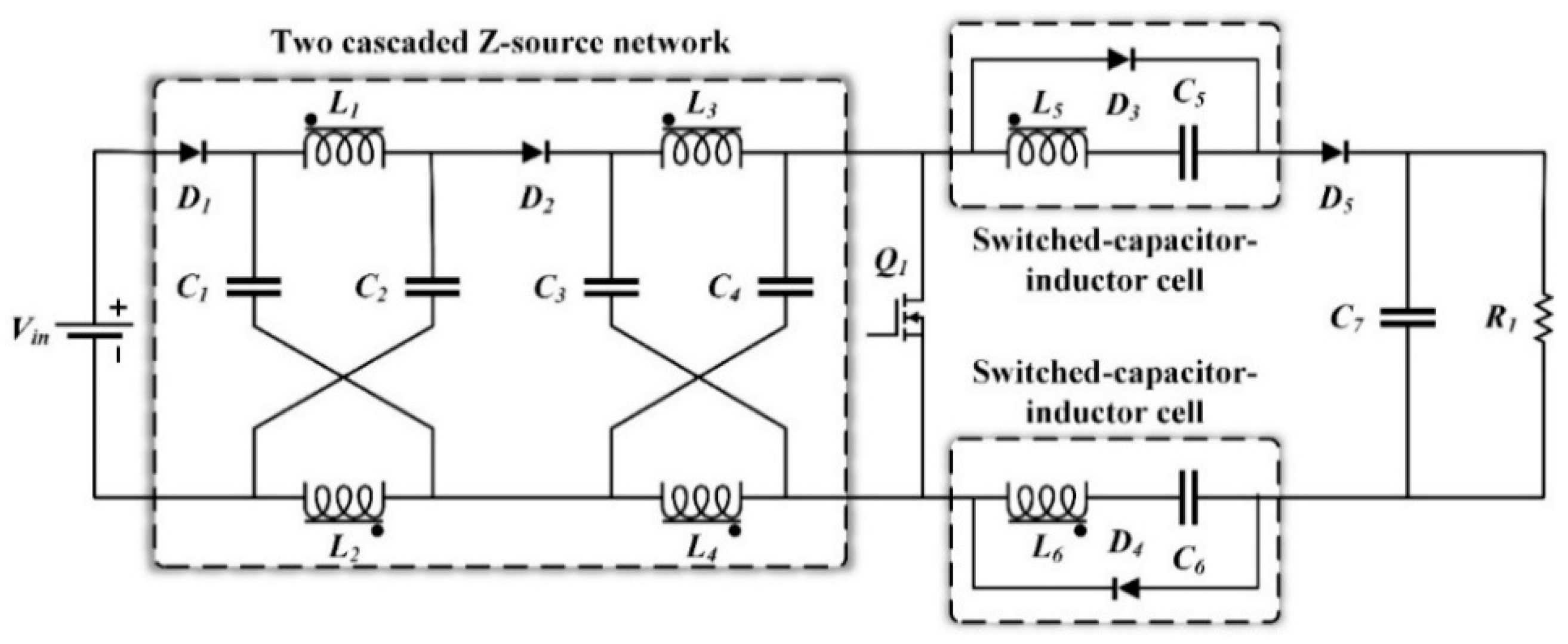
As it can be seen from
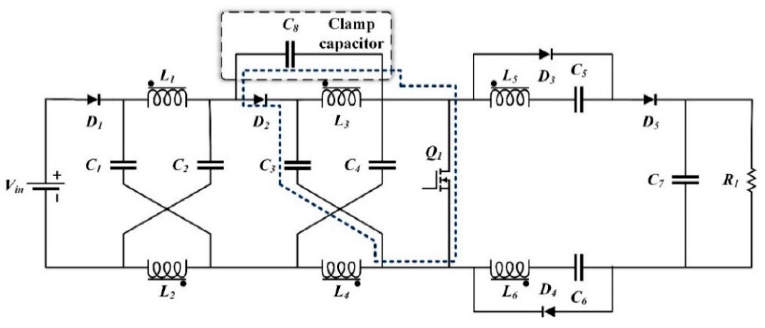
Figure 1, the proposed high step-up DC–DC impedance source based boost converter includes two cascaded Z-source networks and two switched-capacitor-inductor cells. The converter hires a single ferrite core with six coupled inductors, which are part of the impedance network and cells. The very high input current ripple and the high voltage stress of the switch are two main problems in this converter. Therefore, some inevitable alterations are required in order to make the converter practically applicable. Although by adding a capacitor as shown in
Figure 2, the voltage stress of the switch clamps at a specific value, the high input current ripple is still considered as a drawback in this converter. The dashed line in
Figure 2 represents how the KVL (Kirchhoff’s Voltage Law) loop clamps the switch voltage at a specific value. Eventually, the final modification into the converter configuration resulted in obtaining a high step-up converter with low input current ripple and low voltage stress for semiconductor devices.
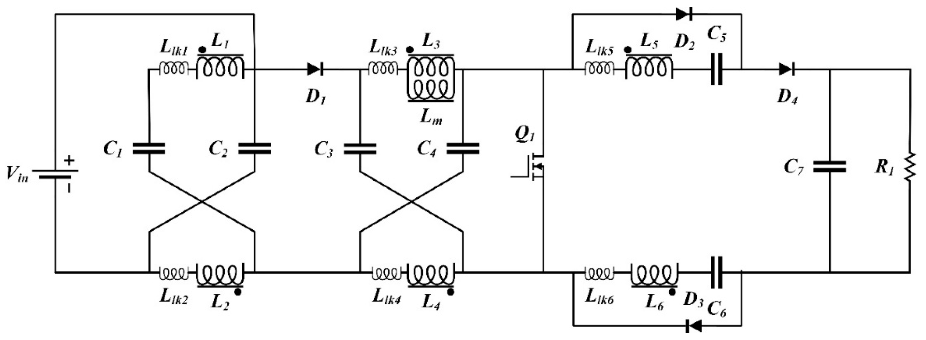
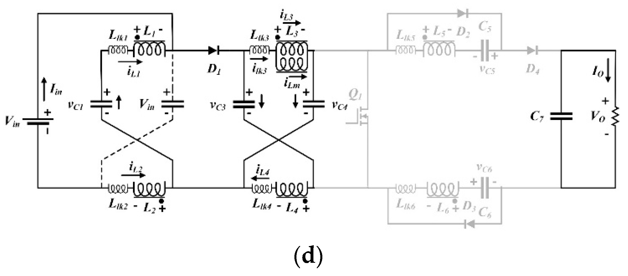
Figure 3 shows the modified proposed high step-up impedance source converter with an equivalent circuit of coupled inductors. The proposed converter is composed of a single switch
Q1; one diode
D1 in the impedance network; two diodes in the cells
D2 and
D3; and one output diode
D4; six coupled inductors
L1,
L2,
L3,
L4,
L5, and
L6; four capacitors
C1,
C2,
C3, and
C4 in the impedance network; two switched-capacitors
C5 and
C6; and output capacitor
C7.
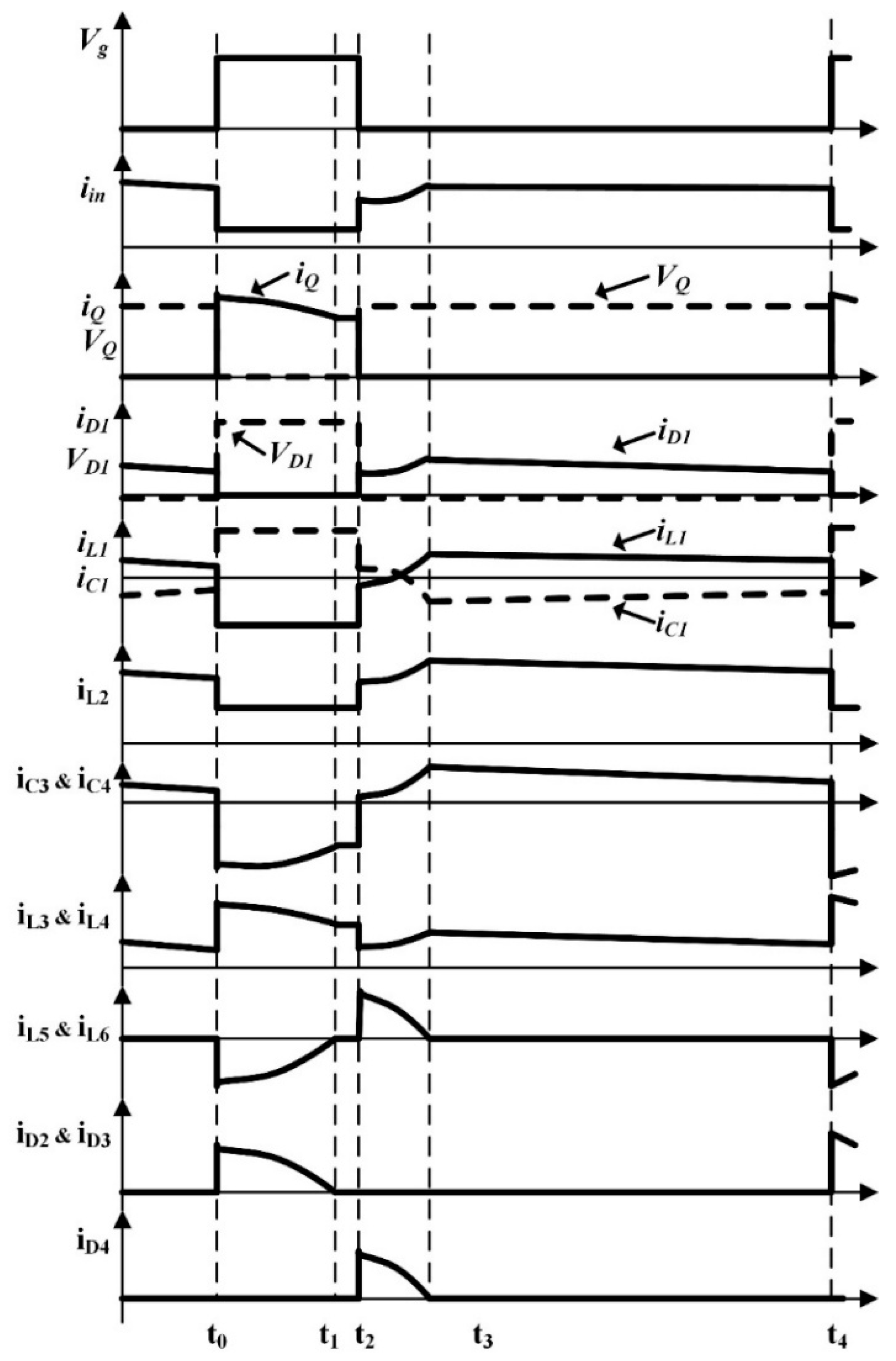
The converter has four time intervals within a switching cycle in the steady state operation.
Figure 4 illustrates the equivalent circuits for each operating interval; the capacitor
C2 can be considered not in the circuit due to being in parallel with input voltage source, and
Figure 5 is provided to show the theoretical waveforms of the proposed converter. To simplify the steady state analysis, the following assumptions are made:
The converter operates in continuous conduction mode (CCM);
The switch, diodes, and all inductors and capacitors are assumed ideal;
The magnetizing inductance is large enough to ignore its current ripple;
The leakage inductances of all windings are equal;
The output capacitor C7 is large enough to make the output voltage constant;
The switching capacitors C5 and C6 are equal.
Operation Principles
Interval 1 [
t0 <
t <
t1] (
Figure 4a): Before the
t0 input, diode
D1 is conducting, and the other semiconductor devices are off. At
t0, the switch
Q turns on, diode
D1 becomes reverse-biased, and (2 +
n)
VC −
Vin is applied across it. In addition, the current direction of capacitors
C3 and
C4 become reverse. In this operation mode, the capacitor voltage of
C3 and
C4 applies to inductors
L3 and
L4, and consequently this voltage will be induced to other coupled inductors
L1,
L2,
L5, and
L6 by considering the turn ratio. In this stage, the energy of leakage inductances
L1 and
L2 are recycled to the input voltage source, and the energy of leakage inductances
L5 and
L6 are absorbed by switched-capacitors
C5 and
C6. The following equations are established in this time interval:
where
n is the turn ratio of coupled inductors:
VC5(
t0) and
VC6(
t0) are less than the coupled inductor’s voltage in their corresponding cells, so a resonance occurs between the leakage inductances and both
C4 and
C5 to charge the capacitors through
D2 and
D3 over the half resonance period. The current and voltage of capacitor
C5 can be expressed as:
where
and
.
The capacitor
C3 and switch
Q current are determined as:
where
iC5 is given by (5).
This mode ends after a half resonance period once the current direction changes. Therefore, the diodes D2 and D3 turn off at zero current.
Interval 2 [
t1 <
t <
t2] (
Figure 4b): At this operation mode, the switch
Q is still on and all diodes are at the off state. In addition, the magnetizing inductance
Lm is still charging by
C3 and
C4. Diodes
D2 and
D3 are off in this stage due to reversing the current of inductors
L5 and
L6, which are blocked by diodes
D2 and
D3, respectively. Therefore, the stored magnetic energy of the transformer leads to slightly increasing the current of other coupling windings. This mode ends when the switch
Q turns off. The current of inductor
L1 can be expressed as:
where
,
, and regarding Equation (5),
I1 is also equal to
iC4(
t1) by considering the turn ratio.
Interval 3 [
t2 <
t <
t3] (
Figure 4c): At
t =
t2, the switch
Q turns off, diodes
D1 and
D4 turn on, and the energy transfers from the input to the output during this stage. The stored energy of the magnetizing inductance and of capacitors
C5 and
C6 also transfers to the load, and capacitors
C3 and
C4 will be charged through diode
D1; however, capacitor
C1 is discharged in this operation mode. The resonance between leakage inductance
L5 and
C5 and also leakage inductance
L6 and
C6 occurs during the maximum time of the half-resonant interval. This stage ends when the resonant current of
iC5 becomes zero and provide the ZCS (zero current switching) turn-off for diode
D4. In the following, the corresponding voltage and current equations are expressed:
Interval 4 [
t3 <
t <
t4] (
Figure 4d): In this stage, the switch is still off and the output diode
D4 is also off by reversing the current of
L5, which occurred in the previous operation mode. However, the input diode
D1 remains on in this stage, which causes the capacitors
C3 and
C4 to keep their charging state on from the previous stage. In addition, capacitor
C1 is discharged the same way as operation mode 3. The current of
L1 can be stated as:
where
I3 is equal to
iC4(
t3) by considering the turn ratio.
Moreover, the other current equations can be expressed as:
This operation mode ends when the switch is turned on again.
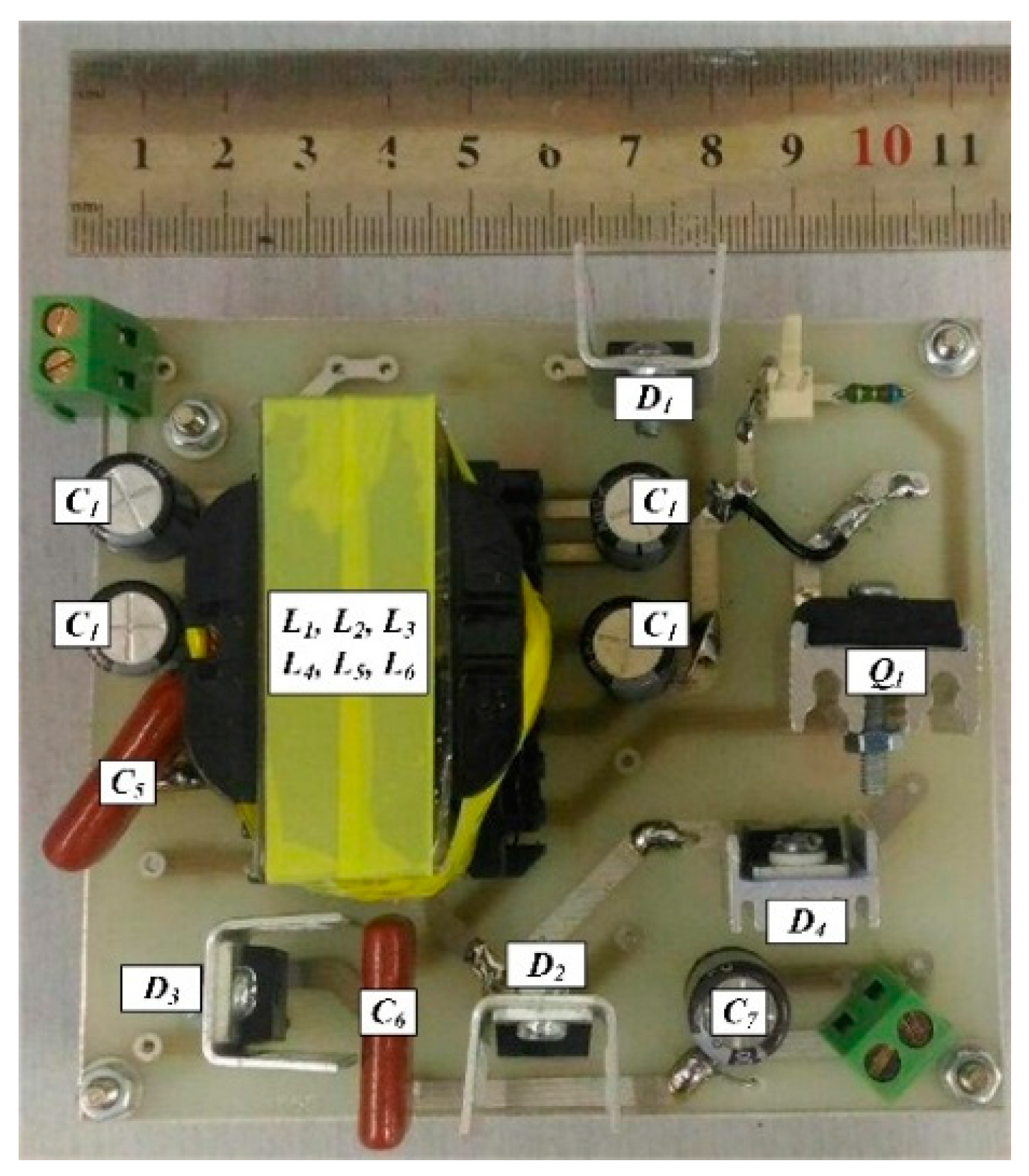
4. Experimental Results
To compare the performance of the proposed converter in practice, a real prototype of the converter was implemented, and experimental results are provided in order to verify the theoretical analysis.
Figure 10 shows the real implemented prototype. The implemented converter operated at 50 kHz to convert the 25 V input voltage to 300 V with a nominal power of 100 W for the load.
Table 2 reports the parameters of the designed converter. The drain-to-source breakdown voltage of the selected MOSFET was much lower than the output voltage, and therefore a low
RDS of the MOSFET resulted in low conduction power loss.
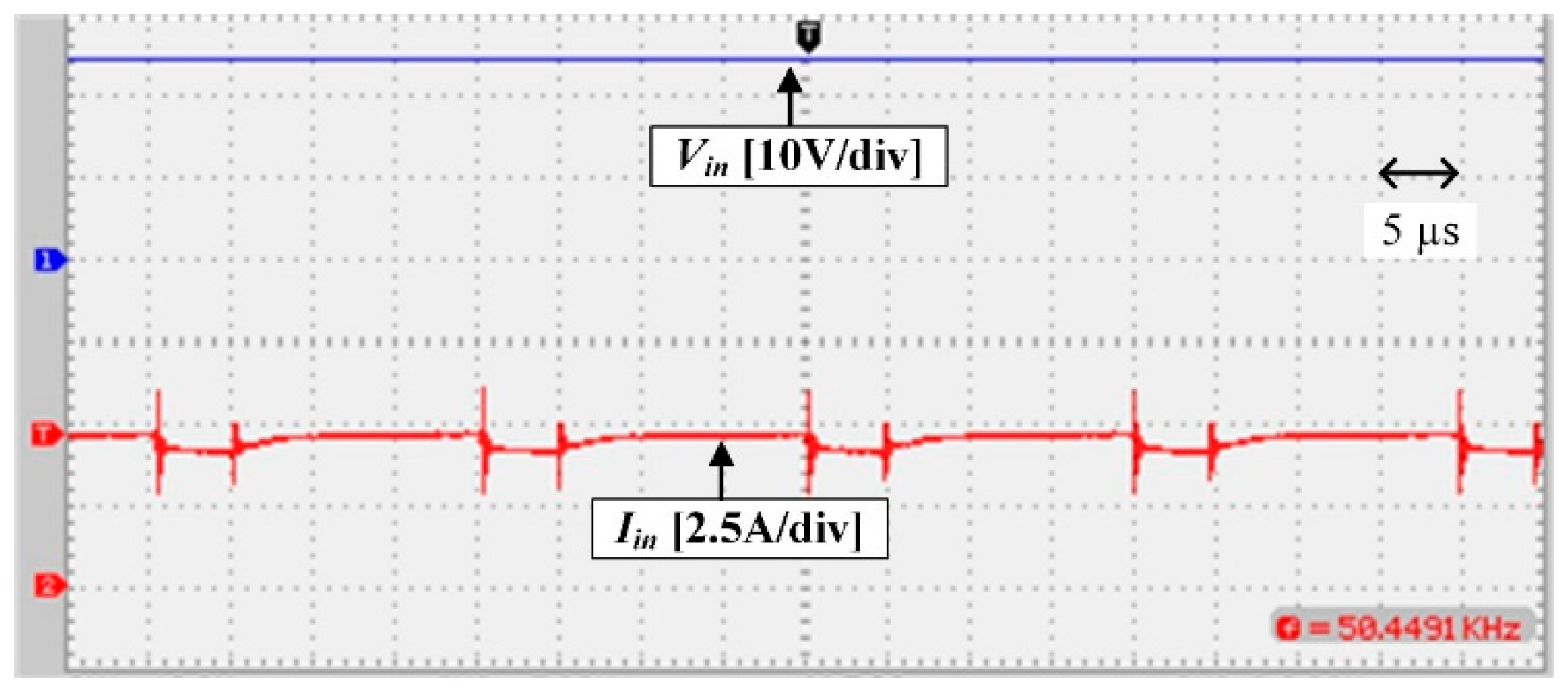
Experimental waveforms of the implemented prototype are illustrated in
Figure 11,
Figure 12,
Figure 13,
Figure 14 and
Figure 15. The input current and voltage of the converter are shown in
Figure 11; the low input current ripple can be observed in this figure.
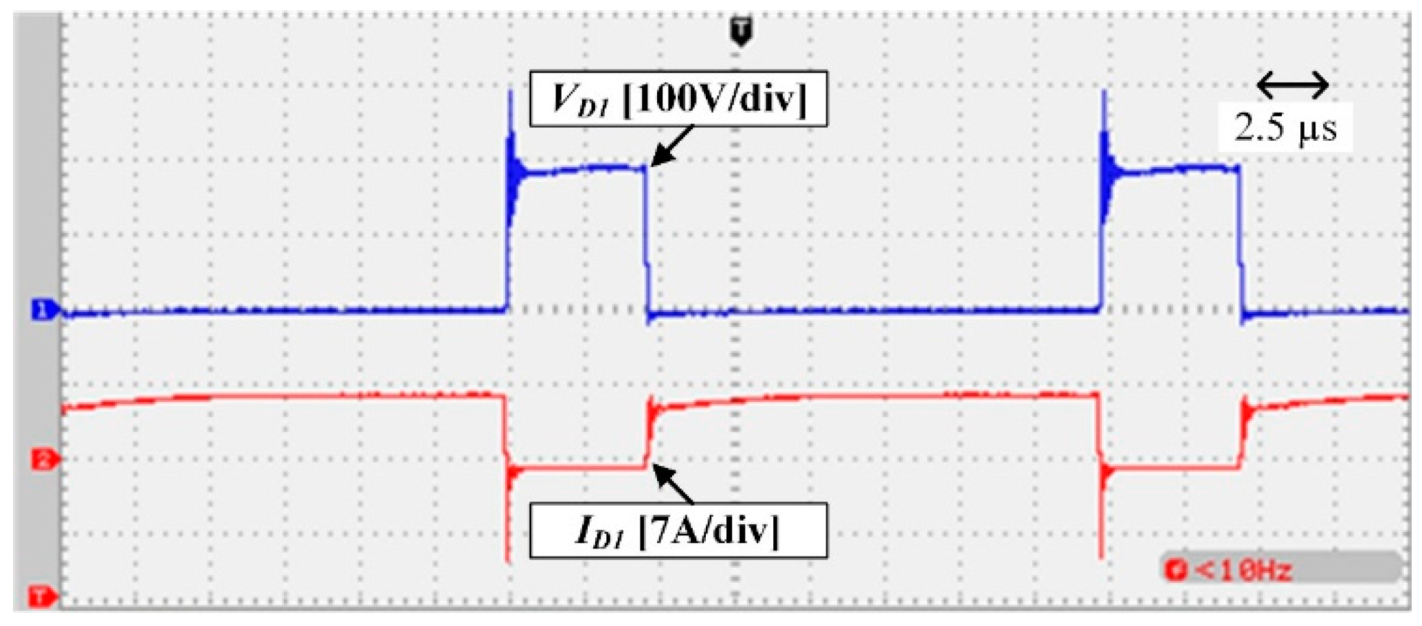
Figure 12 shows the voltage and current of diode
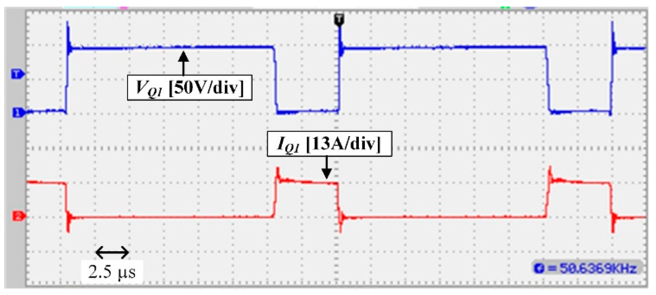
D1; the voltage and current waveforms of the switch are shown in
Figure 13. It can be seen that regarding the output voltage of 300 V, which is illustrated in
Figure 15, the stress voltage of MOSFET is 100 V. Finally, the voltage and current of diode
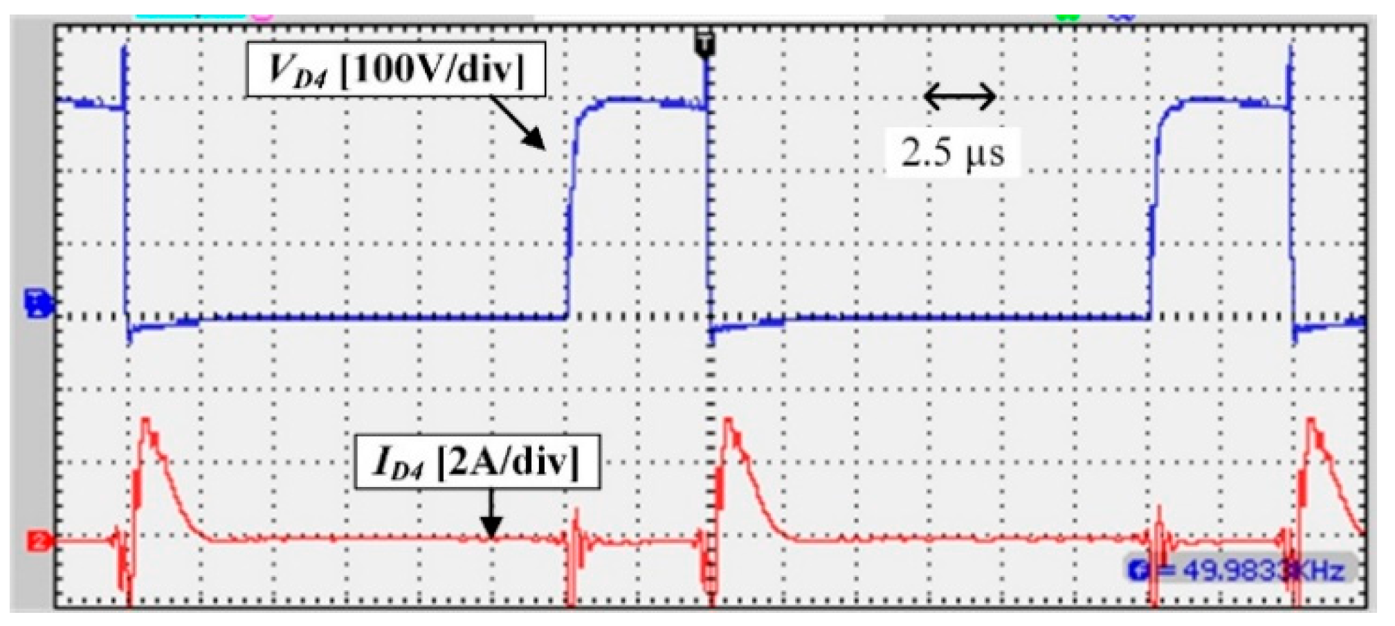
D4 can be seen in
Figure 14.
The efficiency of the proposed converter was calculated by measuring the input and output current and voltage of the converter by means of DC current and voltage meters, respectively.
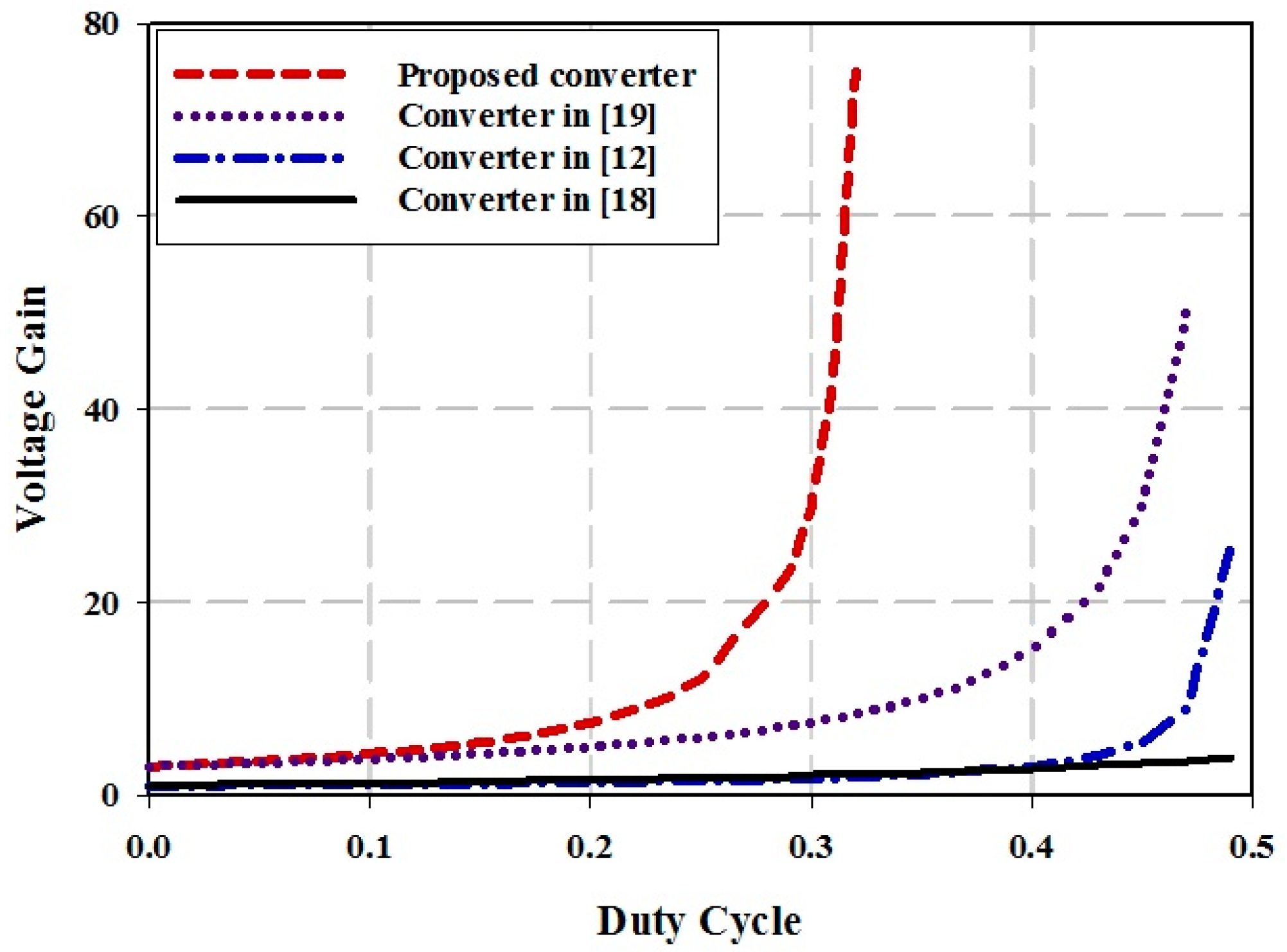
Figure 16 shows the efficiency of the implemented proposed converter from 50% to 100% of a full load condition and it is compared with the converter in [
19]. As it can be observed, by increasing the output power, conduction losses increase as well and lead to dropping the efficiency slightly. Moreover, under a full load condition, the measured efficiency is 93%.


