A New Read Scheme for Alleviating Cell-to-Cell Interference in Scaled-Down 3D NAND Flash Memory


Abstract
:
1. Introduction
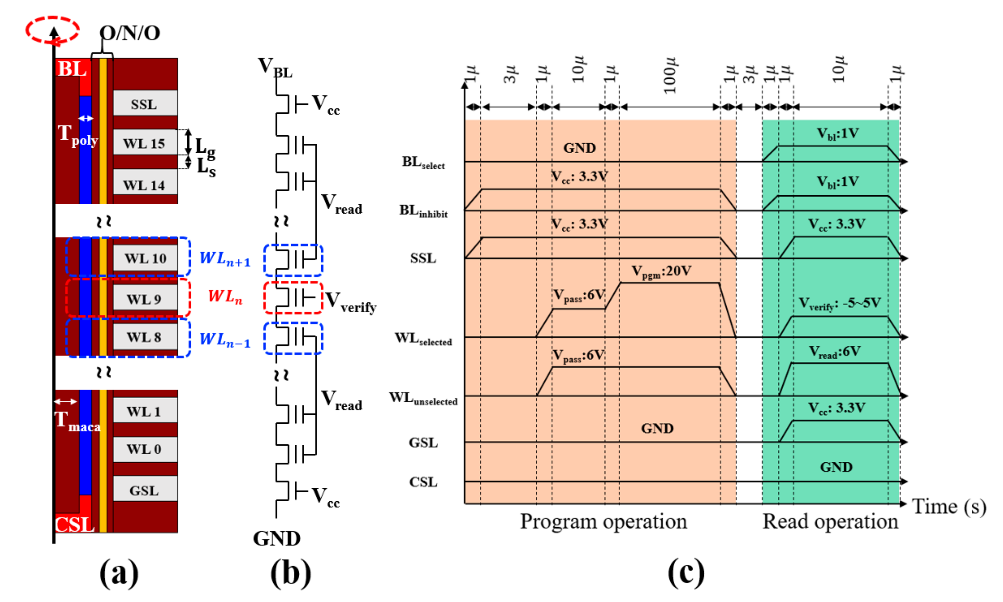
2. Simulation Set-Up
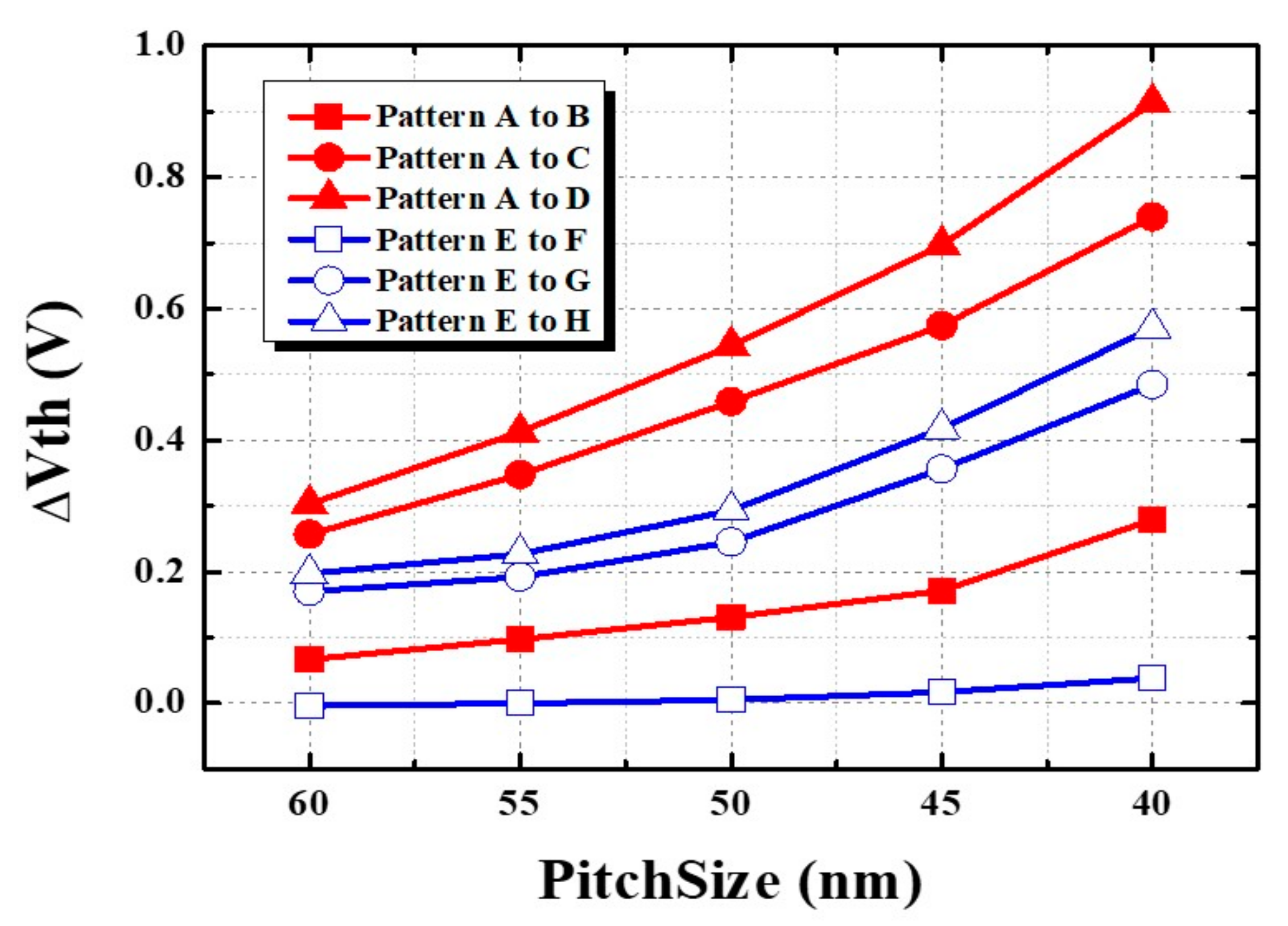
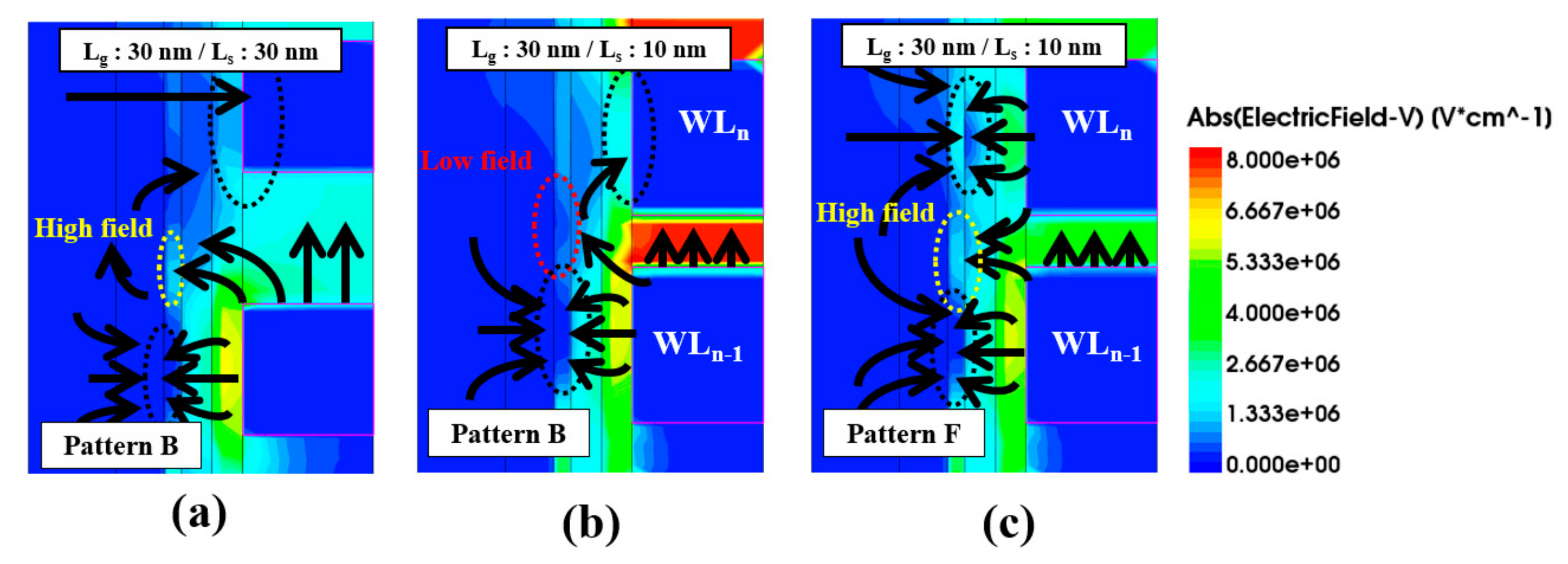
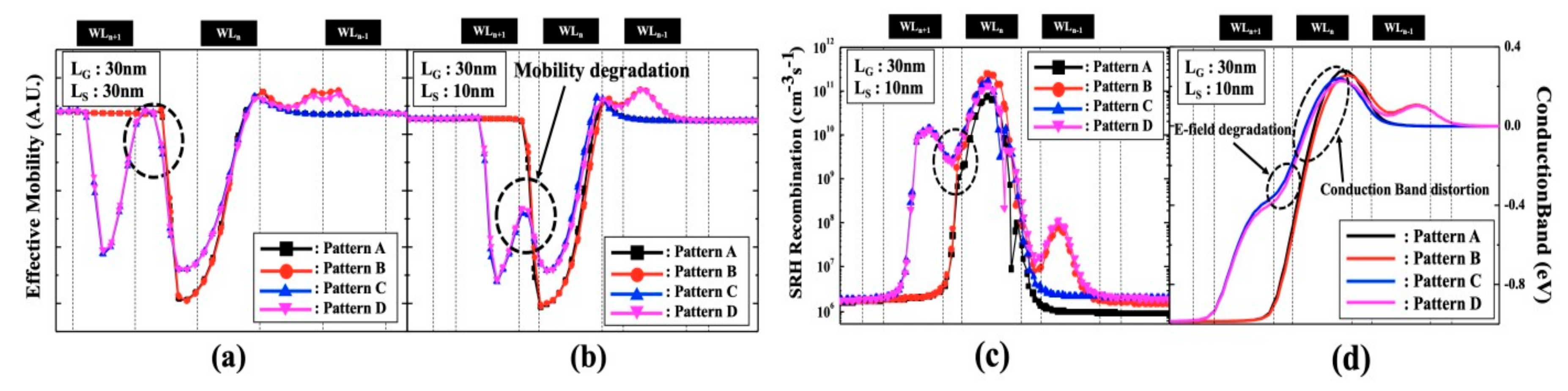
3. Cell-To-Cell Interference
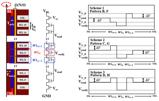
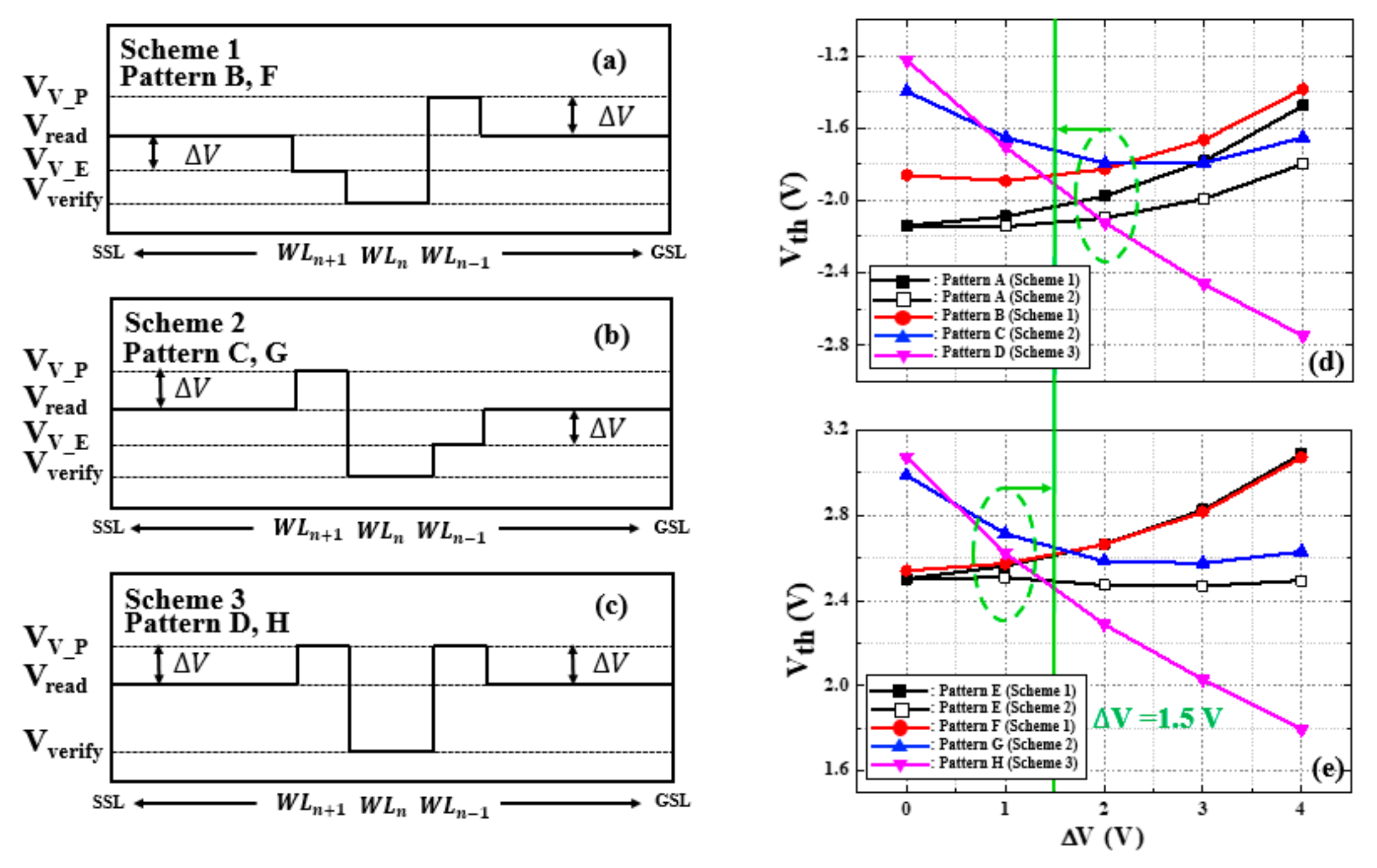
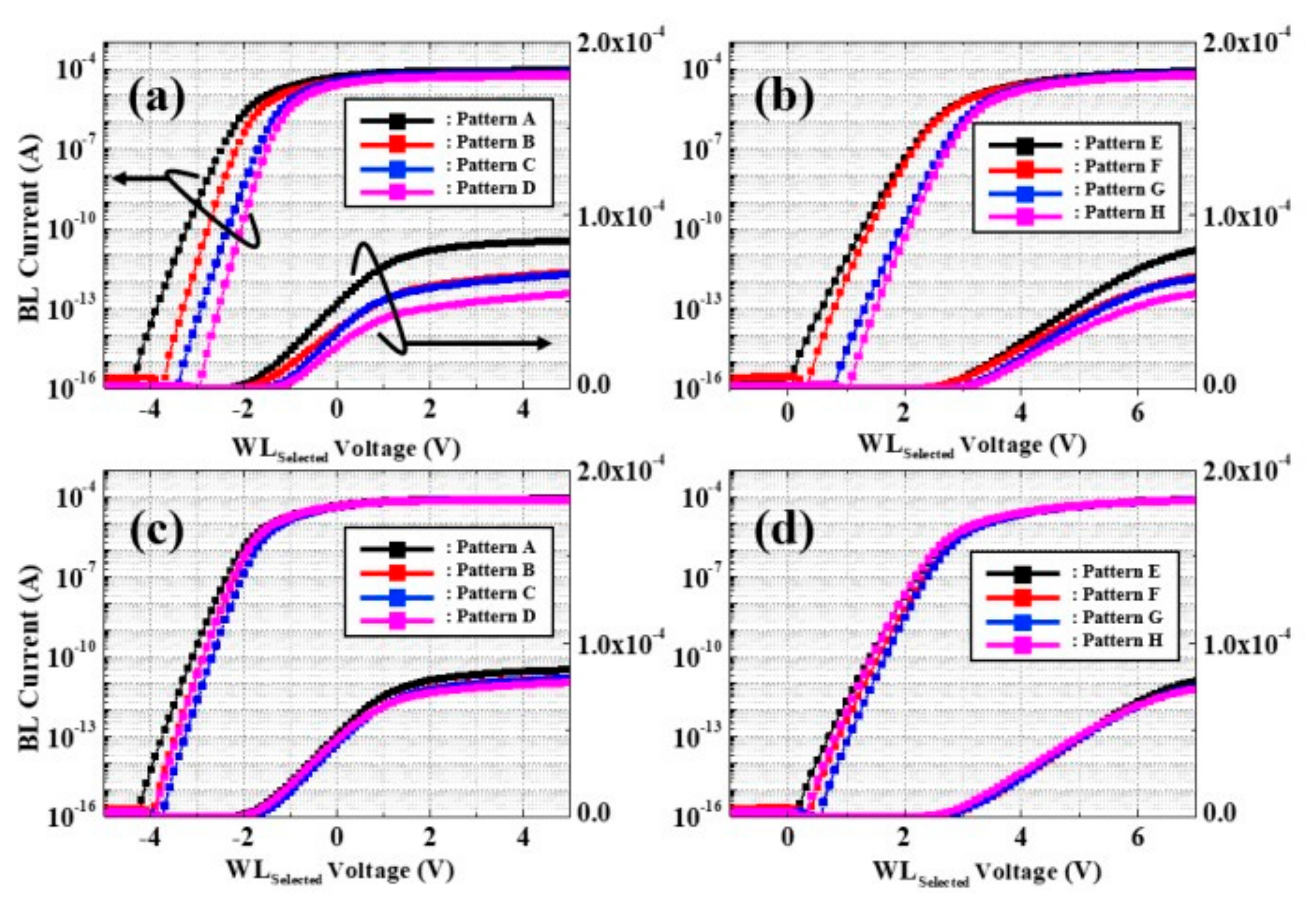
4. Proposed Read Scheme
5. Conclusions
Author Contributions
Funding
Conflicts of Interest
References
- Park, K.T.; Nam, S.; Kim, D.; Kwak, P.; Lee, D.; Choi, Y.H.; Choi, M.H.; Kwak, D.H.; Kim, M.S.; Park, H.W.; et al. Three-Dimensional 128 Gb MLC Vertical nand Flash Memory with 24-WL Stacked Layers and 50 MB/s High-Speed Programming. IEEE J. Solid-State Circuits 2015, 50, 204–213. [Google Scholar] [CrossRef]
- Jeong, W.; Im, J.W.; Kim, D.H.; Nam, S.W.; Shim, D.K.; Choi, M.H.; Yoon, H.J.; Kim, D.H.; Kim, Y.S.; Park, H.W.; et al. A 128 Gb 3b/cell V-NAND Flash Memory with 1 Gb/s I/O Rate. IEEE J. Solid-State Circuits 2016, 51, 204–212. [Google Scholar] [CrossRef]
- Kang, D.; Jeong, W.; Kim, C.; Kim, D.H.; Cho, Y.S.; Kang, K.T.; Ryu, J.; Kang, K.M.; Lee, S.; Kim, W.; et al. 256 Gb 3 b/Cell V-nand Flash Memory with 48 Stacked WL Layers. IEEE J. Solid-State Circuits 2017, 52, 210–217. [Google Scholar] [CrossRef]
- Kim, C.; Kim, D.H.; Jeong, W.; Kim, H.J.; Park, I.H.; Park, H.W.; Lee, J.H.; Park, J.Y.; Ahn, Y.L.; Lee, J.Y.; et al. A 512-Gb 3-b/Cell 64-Stacked WL 3-D-NAND Flash Memory. IEEE J. Solid-State Circuits 2018, 53, 124–133. [Google Scholar] [CrossRef]
- Kang, D.; Kim, M.; Jeon, S.C.; Jung, W.; Park, J.; Choo, G.; Shim, D.K.; Kavala, A.; Kim, S.B.; Kang, K.M.; et al. 13.4 A 512Gb 3-bit/Cell 3D 6th-Generation V-NAND Flash Memory with 82MB/s Write Throughput and 1.2Gb/s Interface. In Proceedings of the 2019 IEEE International Solid- State Circuits Conference—(ISSCC), San Francisco, CA, USA, 17–21 February 2019; pp. 216–218. [Google Scholar] [CrossRef]
- Siau, C.; Kim, K.H.; Lee, S.; Isobe, K.; Shibata, N.; Verma, K.; Ariki, T.; Li, J.; Yuh, K.; Amarnath, A.; et al. 13.5 A 512Gb 3-bit/Cell 3D Flash Memory on 128-Wordline-Layer with 132MB/s Write Performance Featuring Circuit-Under-Array Technology. In Proceedings of the 2019 IEEE International Solid- State Circuits Conference—(ISSCC), San Francisco, CA, USA, 17–21 February 2019; pp. 218–220. [Google Scholar] [CrossRef]
- Jia, X.; Jin, L.; Hou, W.; Wang, Z.; Jiang, S.; Li, K.; Huang, D.; Liu, H.; Wei, W.; Lu, J.; et al. Impact of Cycling Induced Intercell Trapped Charge on Retention Charge Loss in 3-D NAND Flash Memory. IEEE J. Electron Devices Soc. 2020, 8, 62–66. [Google Scholar] [CrossRef]
- Maconi, A.; Arreghini, A.; Compagnoni, C.M.; Van den bosch, G.; Spinelli, A.S.; Van Houdt, J.; Lacaita, A.L. Impact of lateral charge migration on the retention performance of planar and 3D SONOS devices. In Proceedings of the European Solid-State Device Research Conference (ESSDERC), Helsinki, Finland, 12–16 September 2011; pp. 195–198. [Google Scholar] [CrossRef]
- Compagnoni, C.M.; Spinelli, A.S. Reliability of NAND Flash Arrays: A Review of What the 2-D–to–3-D Transition Meant. IEEE Trans. Electron Devices 2019, 66, 4504–4516. [Google Scholar] [CrossRef]
- Goda, A. 3-D NAND Technology Achievements and Future Scaling Perspectives. IEEE Trans. Electron Devices 2020, 67, 1373–1381. [Google Scholar] [CrossRef]
- Hsiao, Y.H.; Lue, H.T.; Chen, W.C.; Chang, K.P.; Tsui, B.Y.; Hsieh, K.Y.; Lu, C.Y. Impact of Vpass Interference on Charge-Trapping NAND Flash Memory Devices. IEEE Trans. Device Mater. Reliab. 2015, 15, 136–141. [Google Scholar] [CrossRef]
- Chen, W.C.; Lue, H.T.; Hsieh, C.C.; Lee, Y.C.; Du, P.Y.; Hsu, T.H.; Chang, K.P.; Wang, K.C.; Lu, C.Y. A physics-based Quasi-2D model to understand the Word line (WL) interference effects of junction-free structure of 3D NAND and experimental study in a 3D NAND flash test chip. In Proceedings of the 2017 IEEE International Electron Devices Meeting (IEDM), San Francisco, CA, USA, 2–6 December 2017; pp. 4.6.1–4.6.4. [Google Scholar] [CrossRef]
- Zhang, Y.; Jin, L.; Jiang, D.; Zou, X.; Liu, H.; Huo, Z. A Novel Read Scheme for Read Disturbance Suppression in 3D NAND Flash Memory. IEEE Electron Device Lett. 2017, 38, 1669–1672. [Google Scholar] [CrossRef]
- Zambelli, C.; Micheloni, R.; Scommegna, S.; Olivo, P. First Evidence of Temporary Read Errors in TLC 3D-NAND Flash Memories Exiting from an Idle State. IEEE J. Electron Devices Soc. 2020, 8, 99–104. [Google Scholar] [CrossRef]
- Kim, Y.; Kang, M. Down-Coupling Phenomenon of Floating Channel in 3D NAND Flash Memory. IEEE Electron Device Lett. 2016, 37, 1566–1569. [Google Scholar] [CrossRef]
- Kang, M.; Kim, Y. Natural Local Self-Boosting Effect in 3D NAND Flash Memory. IEEE Electron Device Lett. 2017, 38, 1236–1239. [Google Scholar] [CrossRef]
- Cho, B.; Lee, C.H.; Seol, K.; Hur, S.; Choi, J.; Choi, J.; Chung, C. A New Cell-to-Cell Interference Induced by Conduction Band Distortion near S/D Region in Scaled NAND Flash Memories. In Proceedings of the 2011 3rd IEEE International Memory Workshop (IMW), Monterey, CA, USA, 22–25 May 2011; pp. 1–4. [Google Scholar] [CrossRef]
- Lee, J.D.; Hur, S.H.; Choi, J.D. Effects of floating-gate interference on NAND flash memory cell operation. IEEE Electron Device Lett. 2002, 264–266. [Google Scholar] [CrossRef]
- Kang, M.; Park, I.H.; Chang, I.J.; Lee, K.; Seo, S.; Park, B.G.; Shin, H. An Accurate Compact Model Considering Direct-Channel Interference of Adjacent Cells in Sub-30-nm NAND Flash Technologies. IEEE Electron Device Lett. 2012, 33, 1114–1116. [Google Scholar] [CrossRef]
- Jung, S.G.; Lee, K.W.; Kim, K.S.; Shin, S.W.; Lee, S.S.; Om, J.C.; Bae, G.H.; Lee, J.H. Modeling of Vth Shift in NAND Flash-Memory Cell Device Considering Crosstalk and Short-Channel Effects. IEEE Trans. Electron Devices 2008, 55, 1020–1026. [Google Scholar] [CrossRef]
- Hsiao, Y.H.; Lue, H.T.; Chen, W.C.; Chang, K.P.; Shih, Y.H.; Tsui, B.Y.; Hsieh, K.T.; Lu, C.Y. Modeling the Impact of Random Grain Boundary Traps on the Electrical Behavior of Vertical Gate 3-D NAND Flash Memory Devices. IEEE Trans. Electron Devices 2014, 61, 2064–2070. [Google Scholar] [CrossRef]


| WLn+1 | WLn | WLn−1 | |
|---|---|---|---|
| Pattern A | ERS | ERS | ERS |
| Pattern B | ERS | ERS | PGM |
| Pattern C | PGM | ERS | ERS |
| Pattern D | PGM | ERS | PGM |
| Pattern E | ERS | PGM | ERS |
| Pattern F | ERS | PGM | PGM |
| Pattern G | PGM | PGM | ERS |
| Pattern H | PGM | PGM | PGM |
Publisher’s Note: MDPI stays neutral with regard to jurisdictional claims in published maps and institutional affiliations. |
© 2020 by the authors. Licensee MDPI, Basel, Switzerland. This article is an open access article distributed under the terms and conditions of the Creative Commons Attribution (CC BY) license (http://creativecommons.org/licenses/by/4.0/).
Share and Cite
Sim, J.-M.; Kang, M.; Song, Y.-H. A New Read Scheme for Alleviating Cell-to-Cell Interference in Scaled-Down 3D NAND Flash Memory. Electronics 2020, 9, 1775. https://doi.org/10.3390/electronics9111775
Sim J-M, Kang M, Song Y-H. A New Read Scheme for Alleviating Cell-to-Cell Interference in Scaled-Down 3D NAND Flash Memory. Electronics. 2020; 9(11):1775. https://doi.org/10.3390/electronics9111775
Chicago/Turabian StyleSim, Jae-Min, Myounggon Kang, and Yun-Heub Song. 2020. "A New Read Scheme for Alleviating Cell-to-Cell Interference in Scaled-Down 3D NAND Flash Memory" Electronics 9, no. 11: 1775. https://doi.org/10.3390/electronics9111775
APA StyleSim, J.-M., Kang, M., & Song, Y.-H. (2020). A New Read Scheme for Alleviating Cell-to-Cell Interference in Scaled-Down 3D NAND Flash Memory. Electronics, 9(11), 1775. https://doi.org/10.3390/electronics9111775